http://dx.doi.org/10.4236/jsip.2014.54021
Adaptive Control of DC-DC Converter
Using Simulated Annealing
Optimization Method
Amin Alqudah
1, Ahmad Malkawi
2, Abdullah Alwadie
31Computer Engineering Department, Hijjawi Faculty for Engineering Technology, Yarmouk University, Irbid, Jordan
2Department of Electrical and Computer Engineering, Faculty for Engineering and Computer Science, Concordia University, Quebec, Canada
3College of Engineering, Najran University, Najran, KSA
Email: [email protected], [email protected], [email protected]
Received 18 May 2013; revised 30 October 2013; accepted 10 November 2013
Copyright © 2014 by authors and Scientific Research Publishing Inc.
This work is licensed under the Creative Commons Attribution International License (CC BY). http://creativecommons.org/licenses/by/4.0/
Abstract
The purpose of this paper is to present a new adaptive control method used to adjust the output voltage and current of DC-DC (DC: Direct Current) power converter under different sudden changes in load. The controller is a PID controller (Proportional, Integrator, and Differentiator). The gains of the PID controller (KP, KI and KD) tuned using Simulated Annealing (SA) algorithm which is part of Generic Probabilistic Metaheuristic family. The new control system is expected to have a fast transient response feature, with less undershoot of the output voltage and less over-shoot of the reactor current. Pulse Width Modulation (PWM) will be utilized to switch the power electronic devices.
Keywords
DC-DC Converter, PID Controller, Simulated Annealing
1. Introduction
present the storage devices. The amount of voltage transferred depends on the duty ratios of the switches [1]. The switch is driven by a pulse width modulator PWM. The output signal of the PWM is controlled using a PID controller. The PID gains are tuned using Simulated Annealing optimizers (SA) to improve the transient re-sponse of the DC-DC converter.
The simulated annealing optimization method is a statistical optimization technique based on a wide random search to achieve global optimum solution with high probability [2]. The idea is based on mimicking the process of annealing a material and then slowly reducing its temperature until a state of thermal equilibrium, which is characterized by minimum energy.
2. Literature Review
Many researchers have worked in the field of controlling DC-DC conversion; in [3] the authors present an im-plementation of the dynamic evolution control with linear evolution path for boost DC-DC power converter. This method uses a simple analysis of non linear equation models of the converter to tune the converter control-lers. This method is used for digital controller to obtain zero steady state error and wide range of stability.
The authors in [4] presented a genetic algorithm-based PID tuning to optimize the performance of the DC-DC converter. A cascade closed-loop control system was implemented consisting of two loops (outer voltage loop inner current loop). The genetic algorithm was used to optimize the gains of the PID controller for the voltage loop.
In [5], the paper conducted high current applications. A DC-DC converter of two stages was studied. The converter consists of two full-bridge inverters both three phase. In this converter a high power factor at the AC stage and a regulated voltage at the DC load are needed. To solve this issue, a control scheme is designed for both inverters. This control scheme is based on a switching function model.
The application of fuzzy control to DC-DC converters operating at finite switching frequency is compared with several control methods like hysteresis and sliding mode method. One of the disadvantages of this fuzzy control is there is no procedure for designing the control rule and the membership functions [6].
The paper in [7] describes a control design procedure for PWM DC-DC converters when there is a large vari-ation in the input reference. The controller has two components: a linear feedback to improve transient response, and a nonlinear feed forward to reject large input disturbances.
3. DC-DC Converter
DC-DC converters are electronic devices used whenever we want to change DC electrical power voltage from one voltage level to another. They are needed because the DC voltage cannot be simply stepped up or down us-ing a transformer as well as AC voltage [1].
Modern electronic systems require high-quality, small size, light-weight, reliable and efficient power supplies. DC-DC converters use power electronics semiconductor switches operating in “on” and “off” states and this is because there is a small power loss in those states; i.e. low voltage in the “on” state, and zero current in the “off” state. In order for the DC-DC converter to be smaller and lighter, the power electronic switches must operate on high operating frequencies. High operating frequencies allow achieving fast dynamic response to rapid changes in the load current and the input voltage [1].
3.1. Step-Down Buck Converter
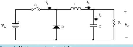
[image:2.595.186.416.633.715.2]The step-down DC-DC converter is known as the buck converter which is shown in Figure 1. It consists of a dc input Vin, a controlled switch S, a diode D, an inductor L, a capacitor C, and a load resistor R.
The switch S is a unidirectional voltage and implemented with power MOSFETs. The relationship between the input and the output voltages and the switch duty ratio D can be illustrated in the following formula with
1
T = f [8].
(
Vin−VO)
DT= −VO(
1−D T)
(1)O
in
V D
V = (2)
The buck converter operation can be divided into two periods; one of them when the switch is “on”, and the other when it is “off” [8].
In the “on” period:
The inductor current can be represented using by:
d d
in C
L V V
i
t = L − L (3)
and the capacitor voltage can be represented by:
d
d
C L C
V i V
t =C−RC (4)
O C
V =V (5)
In the “off” period:
The inductor current can be represented by:
d d
C
L V
i
t = − L (6)
and the capacitor voltage can be represented by:
d d
C L C
V i V
t =C−RC (7)
O C
V =V (8)
where, iL is the current through the inductor, VC is the voltage across the capacitor, Vin is the DC input voltage and VO is DC output voltage.
The above equations can be rewritten in state space as: During “on” time:
1 1 in; O 1
x=A x b V+ V =q x (9)
During “off” time:
2 2 in; O 2
x=A x+b V V =q x (10)
where, d d d d L C i t x V t = ; 1 2 1 1 1 1 L L A A C RC − − = = −
; 1 0 i b L =
; and 2 0 0 b =
Then from Equations (9) and (10):
( )
( )
21 O
in
V s M
L
V s
s s LC
R =
+ +
(11)
3.2. Step-Up Boost Converter
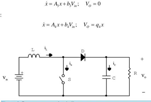
The step-up DC-DC converter is known as the boost converter which is shown in Figure 2. It consists of a dc input Vin, a controlled switch S, a diode D, an inductor L, a capacitor C, and a load resistor R. The switch S is a unidirectional voltage and implemented with power MOSFETs.
The relationship between the input and the output voltages and the switch duty ratio D can be illustrated in the following formula with T =1 f [9].
(
)(
1)
in O in
V DT = V −V −D T (12)
1 1 O
in
V
V = −D (13)
The boost converter operation can be divided into two periods; one of them when the switch is “on”, and the other when it is “off” [9].
In the “on” period: The inductor current is:
d 1
d
L
L in
i R
i V
t L L
−
= + (14)
and the capacitor voltage is:
0
C O
V =V = (15)
In the “off” period: The inductor current is:
d 1 1
d
L
L C in
i R D
i V V
t L L L
− −
= − + (16)
and the capacitor voltage is:
d 1 1
d
C
L C
V D
i V
t C RC
−
= − (17)
O C
V =V (18)
where, iL is current through the inductor, VC is voltage across the capacitor, Vin is DC input voltage and
O
V is DC output voltage.
The above equations can be rewritten in state space as: During “on” time:
3 3 in; O 0
x= A x b V+ V = (19)
During “off” time:
4 4 in; O 4
x= A x+b V V =q x (20)
[image:4.595.168.433.529.708.2]where,
d d d d L C i t x V t =
; 3 4
1 1 1 R D L L A A D C RC − − − = = − −
; 3 4 1
0
b b L
= =
Then from the Equations (19) and (20)
( )
( )
21 O
in
V s M
L
V s s s LC
R = + + (21) where 1 1 M D =
− (22)
4. Control Principles
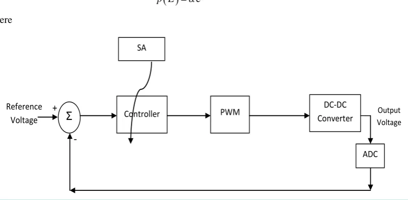
A DC-DC converter must provide a regular DC output voltage under varying load and input voltage. The con-verter values change with time, temperature, and pressure so the controller should be a closed-loop controller with negative feedback. The voltage mode-controller is the most commonly used to control the pulse width modulator PWM [10], as shown in Figure 3.
In the voltage-mode controller the output voltage is sensed and converted to digital signal using ADC, then it is subtracted from a reference voltage to be fed to a controller; this will generate the control signal of the PWM and the PWM signal will drive the controllable switch (MOSFET) of DC-DC converter. The controller is a PID controller; a Simulating Annealing (SA) optimizer will be used to give an optimum PID controller gains. This will improve the transient response when there is a sudden change in the load of DC-DC conver-ter.
4.1. Simulated Annealing Optimizer
Annealing is the process of heating solid bodies high temperature then allowing it to cool down. The mathemat-ical equivalent of annealing is called simulated annealing and described in [2] [11].
The process of simulated annealing is represented based on the probability of Boltzmann distribution of energy E at temperature T as below [12]:
( )
eE KT
p E α
−
= (23)
[image:5.595.99.499.513.709.2]where
Figure 3. The control system of DC-DC converter.
DC-DC Converter PWM Controller
Σ
ReferenceVoltage VoltageOutput
+
1
KT
α = (24)
4.2. Simulated Annealing Algorithm
In this paper, Simulated Annealing is used to find the certain values of among a range of (x, y and z) in order to minimize a certain cost function f x y z
(
, ,)
. The SA algorithm can be summarized as follows [2] [11]:Step 1: Set initial value of T.
Step 2: Select current set values of xi, yi and zi from their ranges randomly.
Step 3: Compute the cost function f x y z
(
i, i, i)
.Step 4: Select other values of xi+1, yi+1 and zi+1 from the same ranges.
Step 5: Compute the cost function f x
(
i+1,yi+1,zi+1)
. Step 6: If the f x(
i+1,yi+1,zi+1)
≤ f x y z(
i, i, i)
then:1
i i
x =x+
1
i i
y = y+
1
i i
z =z+
Step 7: If the f x
(
i+1,yi+1,zi+1)
> f x y z(
i, i, i)
then:If the exp
(
f x(
i+1,yi+1,zi+1)
−f x y z(
i, i, i)
)
T> rand then:1
i i
x =x+
1
i i
y = y+
1
i i
z =z+
Step 8: Reduce the temperature T.
Step 9: Repeat Step 3 to Step 8 for n times to obtain the optimum solution.
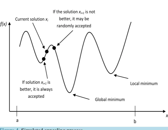
Figure4 shows the simulated annealing process described above. In this work the cost function is:
(
)
( )
0
, , d
S T
p i d
[image:6.595.101.455.132.712.2]f K K K =
∫
te t t (25)Figure 4. Simulated annealing process.
If solution xi+1 is
better, it is always accepted Current solution xi
If the solution xi+1is not
better, it may be randomly accepted
Global minimum
Local minimum
a b x
[image:6.595.158.439.497.715.2]where:
( )
O( )
in( )
e t =V t −V t (26)
5. Results and Discussion [13]
A simulated system of Buck and Boost DC-DC converter was built using MATLAB/SIMULINK toolbox. The DC-DC converter will be controlled using conventional PID controller and this controller will be tuned using Simulated Annealing optimizer. This is used to improve the transient response of the DC-DC converter.
In this work, the Simulated Annealing algorithm is used to tune the gains of the PID controller, which are used to adjust the output voltage and the reactor current. This reduces the undershoot, overshoot and settling time of the output voltage and reduces the overshoot of the reactor current as will be explained next.
5.1. Step-Down Buck Converter Performance
A simulated transient response of a Buck DC-DC converter was built using Matlab Simulink when the load R changed from 100 Ω down to 5 Ω. In this simulation the circuit parameters are as follow: Vin =20 volt,
5 O
V = volt, L=2 mH, C=1000 μF and the switching frequency f =100 KHz.
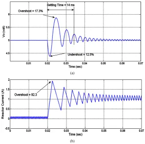
Figure 5 shows the transient response for the conventional PID controller. As shown in the figure, the under-shoot of the output voltage is 12.5%, the overunder-shoot of the output voltage is 17.3%, the settling time is 14 ms and the overshoot of reactor current is 92.3%.
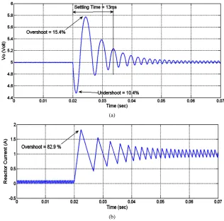
[image:7.595.149.447.402.696.2]Figure 6 shows the transient response for the Simulated Annealing optimizer. As shown in the figure, the undershoot of the output voltage is 10.4%, the overshoot of the output voltage is 15.4%, the settling time is 13 ms and the overshoot of reactor current is 82.9%.
Table 1compares the output based on the conventional PID and the SA output for Buck converter. As can be seen from the table, the output voltage undershoot was reduced, the output voltage over was also reduced. The settling time was slightly reduced and the reactor current over shoot was significantly reduced.
(a)
(b)
(a)
[image:8.595.139.456.83.396.2](b)
[image:8.595.140.470.446.533.2]Figure 6. Transient response of the Simulated Annealing optimizer (a) Output voltage; (b) Reactor current.
Table 1. Conventional PID Vs SA output for Buck converter.
PID SA The improvement
The output voltage undershoot 12.5% 10.4% 16.8%
The output voltage overshoot 17.3% 15.4% 11%
Settling time (ms) 14 13 7.1%
The reactor current overshoot 92.3% 82.9% 10.2%
5.2. Step-Up Boost Converter Performance
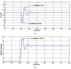
A simulated transient response of a Boost DC-DC converter was built using Matlab Simulink when the load R changed from 100 Ω down to 5 Ω. In this simulation the circuit parameters are as follow: Vin =5 volt, VO =10 volt, L=2 mH, C=2000 μF and the switching frequency f =100 KHz.
Figure 7shows the transient response for the conventional PID controller. As shown in the figure, the under-shoot of the output voltage is 21.1%, the overunder-shoot of the output voltage is 9.9%, and the overunder-shoot of reactor current is 46.1%.
Figure 8 shows the transient response for the Simulated Annealing optimizer. As shown in the figure, the undershoot of the output voltage is 19.8%, the overshoot of the output voltage is 9.7%, and the overshoot of reactor current is 45.5%. As can be noticed, the improvement is minimal in this case.
(a)
[image:9.595.160.437.82.378.2](b)
Figure 7.Transient response of conventional PID controller (a) Output vol-tage; (b) Reactor current.
(a)
(b)
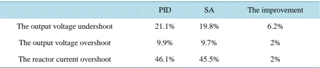
[image:9.595.155.443.413.695.2]Table 2.Conventional PID Vs SA output for boost converter.
PID SA The improvement
The output voltage undershoot 21.1% 19.8% 6.2%
The output voltage overshoot 9.9% 9.7% 2%
The reactor current overshoot 46.1% 45.5% 2%
6. Conclusions
The DC-DC converter is a widely use power electronics circuit. The DC-DC converter output is affected by some parameters changes as load, input voltage, temperature, and the output voltage. So it is very important to use control system technique to improve the output response. One of the most control technique used is the PID controller. Designing a PID controller is complicated. Therefore, in this work we use the Simulated Annealing Optimizer (SA) to design and tune the PID controller gains.
Simulation results of two types DC-DC converters for sudden changes in the load are obtained. As shown in the simulation and results chapter, SA do an efficient improvement in the output in terms of the output voltage undershot, output voltage overshoot and the reactor current. Though, the buck converter got better results.
References
[1] Schimpfle, C.V. and Kirchner, J. (2003) A Step-Down Conversion Concept for a PWM-mode Boost Converter. IEEE Power Electronics, 963-968.
[2] Kirkpatrick, S., Gelatt Jr., C.D. and Vecchi, M.P. (1983) Optimization by Simulated Annealing. Science, 220, 671-680.
http://dx.doi.org/10.1126/science.220.4598.671
[3] Samosir, A.S. and Yatim, A.H.M. (2008) Implementation of New Control Method Based on Dynamic Evolution
Con-trol with Linear Evolution Path for Boost Dc-Dc Converter. IEEE Power and Energy, 213-218.
[4] Wang, X.F., Wu, M., Ouyang, L.Y. and Tang, Q.S. (2008) The Application of GA-PID Control Algorithm to DC-DC
Converter. IEEE Control, 3492-3496.
[5] Kanaan, H.Y., Al-Haddad, K., Georges, S. and Mougharbel, I. (2011) Design, Modelling, Control and Simulation of a Threephase DC-DC Converter for High Currents Applications. IEEE Power Electronics, 424-434.
[6] Lin, B.-R. (1993) Analysis of Fuzzy Control Method Applied to DC-DC Converter Control. IEEE Power Electron, 22- 28.
[7] Garofalo, F., Marino, P., Scala, S. and Vasca, F. (1994) Control of DC-DC Converters with Linear Optimal Feedback and Nonlinear Feedforward. IEEE Power Electronics, 607-615.
[8] Zhang, Y.C. and Hu, Y.M. (2008) On PID Controllers Based on Simulated Annealing Algorithm. Chinese Control Conference, 225-228.
[9] Jeong, G.-J., Kim, I.-H. and Son, Y.-I. (2009) An Adaptive Controller for a DC-DC Boost Converter Considering Load Variation and Coil Magnetic Saturation. APAP Power Electronics, 1-6.
[10] Rashid, M.H. (2011) Power Electronics Handbook. Elsevier Inc., USA.
[11] Kim, Y. and Kim, H. (1990) A Stepwise-Overlapped Parallel Simulated Annealing Algorithm, Integration. The VLSI Journal, 10, 39-54. http://dx.doi.org/10.1016/S0167-9260(05)80034-3
[12] Corana, A., Marchesi, M., Martini, C. and Ridella, S. (1987) Minimizing Multimodal Functions of Continuous Va-riables with the Simulated Annealing Algorithm. ACM Transactions on Mathematical Software, 262-280.
http://dx.doi.org/10.1145/29380.29864