© 2017, IRJET | Impact Factor value: 5.181 | ISO 9001:2008 Certified Journal | Page 329
Multi-power rail FLR configurable for Digital Circuits
P.RAJASRI
1, MOHAMMAD TAJ
2and K GOVINDA RAJULU
31. Dept. of ECE, Eluru College of Engineering and Technology, Eluru.
2. Assistant Professor, Dept. of ECE, Eluru College of Engineering and Technology, Eluru
.
3. HOD & Associate Professor, Dept. of ECE, Eluru College of Engineering and Technology, Eluru
.
---***---Abstract—
To overcome the constraints onpower distribution, silicon area, quiescent current and minimum required efficiency, a multi-power rail FLR is proposed. This FLR uses dual 1.8V and 3.3V rails with an overall improvement of 40% of the power efficiency when operating at low voltage (1.0 V) compared to the solution with only a single 3.3 V rail. The architecture is optimized to operate at low voltages (such as 1.0 V) where 80% of the current is provided by the 1.8 V rail. This contribution from the lowest voltage rail to the output current drastically decreases as the output voltage gets close to 1.5 V, where the 3.3 V rail supplies most of the power. Notice that no mechanism is provided in this circuit to limit the current from the power supplies. A complementary solution is proposed in this presented paper where a single rail can be selected to minimize heat dissipation and silicon area. With the solution proposed as a silicon area similar to that reserved for the power transistors will be used, where power rails are scaled down to handle only half the maximum current capability of the solution. This architecture benefits from a configurable control loop, power supply and bulk biasing. The principle is that when lower output voltages are required at the NanoPad, the 1.8 V rail is activated for a maximum theoretical efficiency from 55% up to 83% (1.0 and 1.5 V output voltages).
Index Terms—FLR, Configurable, multi-power rail, NanoPad, voltage regulator.
1
INTRODUCTION
the solution proposed in fig-1,a silicon area similar to that reserved for the power transistors where power is scaled down to handle only half the maximum current capability of the previous solution biasing. The principle is that when lower output
voltages are required at the NanoPad, the 1.8V rail is activated for a theoretical efficiency from 55% up to 83% (1.0 and 1.5V output voltages).
A challenge with multi power rail systems is the potential for latch up. To prevent any possibilities of latch up, protection transistors (switches) were added. With these transistors,it is possible to ensure that only one power rail at a time is tapped. Specifically, transistors M14 must be turned off when VOUT is larger
than the branch power supply VDDn.M14 is turned off
using the voltage VBASE that provides static bulk biasing
for M13 and M14 and that also feed the control loop with the suitable supply voltage.
When the VDDn rail is in operation M13-M14 bulks
(VBASE) are set to VDDn. When not in operation the bulks
are biased at the highest voltage,Vdd1. Table
[image:1.595.311.557.457.696.2]Fig. 1 Multi-power rail FLR sharing a common configurable control loop.
TABLE I COMPARISON OF REVIOUSLY REPORTED AND PROPOSED SOLUTION OF POWER FOR A SINGLE OR MULTI-POWER-RAIL
© 2017, IRJET | Impact Factor value: 5.181 | ISO 9001:2008 Certified Journal | Page 330 described in this section. It shows that for the same
silicon area the proposed solution offers an extended output range,better power efficiency ,and comparable I/O speed but at the cost of a smaller maximum output per rail(50mA instead 110mA). However,the same power is still available throughout the whole digital system.
2 Circuit Implementation
This section details the circuit implementation for the pro- posed the multi-power-rail voltage regulator and I/O. It corre- sponds to a fabricated dual power rail, which can be extended
to a multi-power rail configuration. The proposed architecture combines two separate fast load regulators operating with two power supplies (1.8 and 3.3 V). It is possible to operate one FLR at a time while sharing the same voltage feedback loop. Switches and dynamic bulk biasing are also added to prevent latch-up and ensure a good isolation of the non-operating FLR. The total current budget can be divided by the number of imple- mented power rails. In our particular case, a 110 mA total pos- sible current is divided over 2 power rails occupying the same silicon area. This multi-power-rail regulator uses one common voltage reference generated in each Unit-Cell by a configurable band gap in the master stage (Fig. 1) . This band gap based voltage reference nominally produce the same voltage throughout the entire silicon wafer, in order to produce a steady operating voltage on Vout when the temperature increases or when there are slow variations ( kHz) in the power supplies.
A. Multi-Rail Voltage Regulator Circuits
Fig. 2. Transistor level of the proposed configurable multi-power rails FLR with 1.8 and 3.3 V power rails.
the regulator can be configured to use either one of the two implemented supply rails, which are designed to operate at 1.8 V and 3.3 V, in order to limit the energy dissipated into the Digital system.
3 Single Rail Configurable I/O PAD
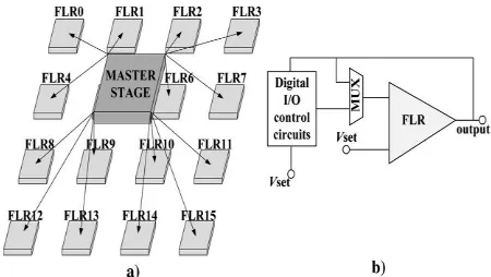
The design proposed takes advantage of a hierarchical topology in order to minimize quiescent current and silicon area consumption by sharing the maximum number of common circuitries. A master – slave topology is used in every unit-cell. In reference to fig (3), the top module uses a reference voltage (VSET)
shared between 16 NanoPads. The fast load regulator (FLR) embedded in each NanoPad (fig1.3) uses VSET to
set the output voltage within the range of 1.0V to 2.5V. In addition, VSET sets the digital I/O voltage levels. This
technique leads to a reduction in silicon area by sharing fast load regulator with the digital I/O to provide power through configurable voltage (VSET),
which avoids duplicating power stages for supplying the digital I/O.
Fig. 3 (a) The master-slave topology proposed where a master stage feeds to 16 fast load regulators (FLR) a common reference voltage. (b) The embedded digital I/O where the feedback signal is either controlled by the FLR or the digital I/O control circuits.
[image:2.595.343.568.450.577.2]© 2017, IRJET | Impact Factor value: 5.181 | ISO 9001:2008 Certified Journal | Page 331 The configurable I/O pad proposed in (fig 3)
integrates a digital I/O within the regulation loop coupled with a boost technique using a differential pair. The digital I/O can be configured to fit standard CMOS voltages of 1.0,1.2,1.5,1.8,2.0, 2.5 and 3.3V with a post layout simulated bandwidth of over 300MHZ with a 5pF load.This approach allows very high current capabilities within a unit cell that could supply more than 100mA per NanoPad,with a theoretical 1.6 A maximum per unit-cell (16 FLR according(fig 3), with adequate integrated power.
This is due to the fact that the maximum power efficiency of a linear regulator is (VOUT)2/(VDD)2 This
fact limits the one rail approach in terms of the maximum output power that every NanoPad can provide within a small silicon area (such a unit-cell)
4 A Multi-rail Power Supply for Power
Efficiency Improvement
To maximize efficiency of the embedded FLR a multi-power supply rail where a multilevel converter using a single rail is used to generate several output voltage levels using a multiplexed voltage supply or stack voltage cells (independent cells put in series where the output voltage is a combination of them).this multi-rail approach can increase the power efficiency by 49%. This efficiency depends on the source power supply and output voltage,with a maximum of 50W of instantaneous power. Unfortunately this approach uses discrete components that make it incompatible with our embedded FLRs, where a fully integrated solution is required.
5 POWER DISTRIBUTIONS
Power distribution presents several significant problems.
Fig.4 A floorplan that isolates a ground pin
First, we must design a global power distribution network that runs both VDD and VSS entirely in metal. Second, we must size wires properly so that they can handle the required currents. Third, we must ensure that the transient behavior of the power distribution network does not cause problems for the logic to which it supplies current. While keeping all these problems in mind, we must tackle two types of power supply loss:
• IR drops from steady state currents;
• Drops from transient current.
5.1 POWER DISTRIBUTION TYPES
The predominant types of power distributions in use are
H-tree
A Balanced Clock Tree
Grid
5.5.1 H-tree
The H tree is a very regular structure which allows predictable delay. The balanced tree takes the opposite approach of synthesizing a layout based on the characteristics of the circuit to be clocked.
Fig.5 H tree
© 2017, IRJET | Impact Factor value: 5.181 | ISO 9001:2008 Certified Journal | Page 332 widths of the wires in the H tree can be adjusted to
account for variations in load capacitance to equalize skew throughout the H tree. Buffers can also be added into the H tree network to increase drive capability.
An H tree network can be thought of as a top-down clock distribution methodology since the floorplan of the H tree determines the floorplan of the logic to which it is connected. Since skew increases with physical distance in the H tree, memory elements must be grouped together to make use of the same or nearby distribution points in the H tree network.
5.5.2 A Balanced Clock Tree
A Balanced Tree Clock network, illustrated in Figure 6, is generated by placement and routing. Memory elements are clustered into groups. The clustering is used to guide placement and a clocking tree is then synthesized based on the skew information generated during clustering. The tree is irregular in shape but has been balanced during design to minimize skew.
Fig 6A Balanced Clock Tree
Once again, wire widths can be varied in the tree and buffers can be added. Several tools exist for generating balanced clock trees.
5.5.3 Grid
[image:4.595.310.537.99.216.2]A processor will have a large number of these local points and will require a large number of branches and therefore a deep distribution tree. A deep distribution tree will exhibit large POD delays and degraded clock performance. Subdividing the die into a smaller number of clock regions and applying a grid to serve each region can be a superior solution.
Fig 7 Grid Distribution
Figure 7 schematically shows a 2-dimensional grid serving one of these clock regions. This clock grid resembles a mesh with fully connected clock tracks in both dimensions and grid drivers located on all four sides. Local loads within a region can be directly connected to the grid. The grid effectively shorts the output of all drivers and helps minimize delay mismatches.
Figure 2.6 shows an idealized delay profile of a 2-dimensional grid assuming uniform loading. The shorted grid node helps balance the load non-uniformities and results in a more gradual delay profile across the region. Additionally, since the grid drivers are shorted, the POD delay to all the loads within a region is limited to the interconnect delay of the grid which is typically small and results in lower clock skew uncertainty across the region.
6 Introduction to DSCH
The DSCH2 program is a logic editor and simulator. DSCH2 is used to validate the architecture of the logic circuit before the microelectronics design is started. DSCH2 provides a user-friendly environment for hierarchical logic design, and fast simulation with delay analysis, which allows the design and validation of complex logic structures.Some techniques for low power design are described in the manual. DSCH also features the symbols, models and assembly support for 8051 and 18f64. DSCH also includes an interface to SPICE.
7 Introduction to MICROWIND
[image:4.595.75.281.415.553.2]© 2017, IRJET | Impact Factor value: 5.181 | ISO 9001:2008 Certified Journal | Page 333 simulate. MICROWIND2 includes all the commands
for a mask editor as well as original tools never gathered before in a single module (2D and 3D process view, VERILOG compiler, tutorial on MOS devices). You can gain access to Circuit Simulation by pressing one single key. The electric extraction of your circuit is automatically performed and the analog simulator produces voltage and current curves immediately.
8 SIMULATION RESULTS
The schematic diagram is drawn using the DSCH2 software.
First, the requiredcomponents for the
circuit are placed by drawing them
from the symbol palette available as a
sidebar in the DSCH software.
After completion of the circuit, save the
file with .SCH extension.
Go to File menu and click ‘Make a
Verilog file’ option to generate a verilog
program for the designed circuit.
The circuit drawn using DSCH software
is shown in fig.8
Layout diagram is drawn using the
MICROWIND software.
First, go to the comple menu and select
the option ‘compile a verilog file’.
Then a dialogue box gets opened
Fig.8 Schematic Circuit
Fig.9 Layout diagram
9 CONCLUSION
© 2017, IRJET | Impact Factor value: 5.181 | ISO 9001:2008 Certified Journal | Page 334 This paper focuses on means for power delivery
that mitigate heat dissipation by introducing a novel multi power rail voltage regulator that operates from1.8V and 3.3V rails. The addition of second power rail allows power savings up to 25%,while offering a wider range of operation at the cost of reducing the total deliverable power per rail due to limitations in the available area. The proposed design mergestwo fast load regulators into one by using configurable power supplies,the bulk biasing technique and shared transistors. The proposed architecture was fabricated in a 0.12µm CMOS technology and occupies a small area of 0.0075mm2
by combining the two control loops into one, which makes it suitable for wafer scale integration. Moreover,the proposed design offers a fast response time of 11ns, with a 35mA load on either supply rail or very low quiescent currents of 120µA. This work also achieves the best figure of merit that outperforms by a factor of 3 its closest competitors.
10 REFERENCES
1.Laflamme-Mayer.N, Blaquiere.Y, Savaria.Y,
Sawan.M, "A Configurable Multi-Rail Power and
I/O Pad Applied to Wafer-Scale Systems," Circuits and Systems I: Regular Papers, IEEE Transactions on , vol.61, no.11, pp.3135,3144, Nov. 2014
2. A textbook on “Modern VLSI Design- IP Based
Design” by Wayne Wolf - Prentice Hall Modern Semiconductor Design Series- Fourth Edition.
3.Norman.R, Valorge.O, Blaquiere.Y, Lepercq.E,
Basile-Bellavance.Y, El-Alaoui.Y, Prytula.R,
Savaria.Y, "An active reconfigurable circuit
board," Circuits and Systems and TAISA Conference, 2008. NEWCAS-TAISA 2008. 2008 Joint 6th International IEEE Northeast Workshop on, vol., no., pp.351,354, 22-25 June 2008.
4.Laflamme-Mayer.N, Andre.W, Valorge.O,
Blaquiere.Y, Sawan.M, "Configurable Input–
Output Power Pad for Wafer-Scale Microelectronic Systems," Very Large Scale Integration (VLSI) Systems, IEEE Transactions on , vol.21, no.11, pp.2024,2033, Nov. 2013
5.Valorge.O, Andre.W, Savaria.Y, Blaquiere.Y,
"Power supply analysis of a largearea integrated
circuit," New Circuits and Systems Conference (NEWCAS), 2011 IEEE 9th International , vol., no., pp.398,401, 26-29 June 2011
6.Hazucha.P, Karnik.T, Bloechel.B.A, Parsons.C,
Finan.D, Borkar.S, "Area-efficientlinear regulator