LOW POWER AND HIGH PERFORMANCE HYBRID-CONTENT
ADDRESSABLE MEMORY (CAM) IN SOI-TECHNOLOGY
Abdulla Onathukattil and Harish M Kittur VLSI Design, SENSE, VIT University, Vellore, India
E-Mail: [email protected]
ABSTRACT
Low power consumption and high speed are the two major concerns related to the design of CAM (Content Addressable Memory). In this paper, we combined the performance advantage of NOR-type CAM with power efficiency of NAND-type CAM which is termed as Hybrid-CAM. It is implemented using 30 nm SOI technology utilizing the BSIM model for SOI. Each CAM word is divided into two segments in which one segment is implemented using NAND-type and the other using NOR-type. The realized hybrid-CAM, based on 30 nm 0.9V SOI, achieves a 93% power reduction and 47% performance improvement As compared to the traditional NAND-type and NOR-type CAM cells implemented on SOI technology.
Keywords: content addressable memory, BSIM-SOI, NAND-type, NOR-type, hybrid-type CAM.
INTRODUCTION
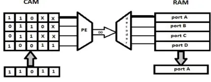
Content addressable memories (CAM) are storage which is addressed by data compared to storage memory which is addressed by addresses. Because of its parallel comparison capability, it is one of the important elements in network routers, data compression; image processing etc. the commercial application includes the classification and forwarding of IP (Internet Protocol) packets in network routers. In network like internet large messages are broken down into small packets and sending each of it individually through network. These packets are routed from source to destination by routers and reassembled at destination. Since CAM is a functional memory with large storage and simultaneous search capability of comparing the search address against the table of stored address, it is used in the network routers to identify the port address of the incoming packet with a destination address. The basic CAM implementation of routing table is given in the Figure-1.
[image:1.612.78.293.622.706.2]There is mainly two conventional type CAM design, they are NOR-type and NAND-type CAMs. The NAND-type has low power consumption where the NOR-type has best search performance but high power consumption. Hybrid-type Cam design combines the performance advantage of NOR-type CAM with power efficiency of NAND-type CAM. The major power consumer in CAMs are match line (ML), the power consumption can be reduced by the small voltage swing on match line and dividing the match line. Both techniques have less power but the major drawback is performance degradation.
Figure-1. Basic CAM implementation of routing table.
The main features of Hybrid-type CAM are
It is not required to discharge the search lines so that short circuit power consumption is greatly reduced.
Match Line (ML) is decoupled from the CAM cells. So the ML discharges only when there is matching which makes the ML less contributor of power consumption.
Match Line discharge are speed up by the fast pull down path if there is a word match and is independent of the segment size.
The level restorer path provides additional immunity to the match incurred by the race condition.
However the speed improvements and less power reduction is achieved at the expenses of increased silicon area and device scaling. Till now, the device performance is increased by combining the device scaling, material property improvement and new device structures. But it has reached to its fundamental limits. The conventional CMOS technology is suffering mainly from physical limitation in sub-micron or nanometer region which leads to the alternative new technology called SOI (Silicon on Insulator). It has many advantages compared to existing BS (bulk Silicon) CMOS technology like high speed, high radiation tolerance, low parasitic capacitance, low short channel effects etc. BSIM.
form.
The rest of the paper is organized as follows. Section II reviews conventional CAM organization, its advantages and disadvantages. Section III explains about SOI technology, its various types and its advantages. Section IV tells about the implementation of Hybrid CAM using FD-SOI and its operation in detail. Finally the results and comparison is done in section V.
CAM ORGANIZATION
CAM (Content Addressable Memory) has mainly two parts, they are store unit and compare unit. The store unit is implemented as 6T SRAM cell and compare unit is pass transistor implementation of either XOR or XNOR function to compare the stored data with the input data. Besides the store and compare unit there is a pull-down transistor whose gate is connected to the comparison result. This transistor decides whether the ML has to connect or disconnect to ground based on the comparison result. Basic CAM cells are given below in Figure-2 and Figure-3.
Figure-2. XNOR-type CAM cell.
CAM operation begins with pre-recharging all ML (Match Line) to high and placing the search data on differential search lines. Match Line remains high state if all cells are matched otherwise it is discharged to low. There are mainly two type of CAM design. They are NAND-type and NOR-type. Its operation is explained below.
Figure-3. XOR-type CAM cell.
NAND-type Design
In this type the CAM-cell are usually XNOR-type and the pull down transistors are connected in NAND-type. As shown in Figure-4, ML is initially pre-charged to high, if all bits of word are matched then ML is discharged to 0. Since pull down transistors are connected in series load capacitance of ML is low thereby low power consumption. But it takes long time to discharge ML in case of match. So NAND-type design has better power efficiency for performance degradation.
Figure-4. NAND type design.
NOR-type Design
In this CAM-cells are usually XOR-type instead of XNOR. Here the pull down transistor is arranged NOR-type as shown in Figure-5. During pre-charge phase the ML is initially pre-charged to high. For a CAM word if there is a miss-match in any one of the cell, the ML is discharged to zero. Otherwise it remains high state if and only if all bits of word is matched. Since pull down path is very short in case of miss-match, these type of design gives better search performance. It consumes more power because ML has large capacitance due to the parallel nature of pull down transistors.
Figure-5. NOR-type design.
SOI TECHNOLOGY
In SOI (Silicon On insulator), the transistors are formed on a thin silicon layer which is insulated from the substrate by an electrical insulator usually silicon dioxide (SiO2). The insulating layer is referred as ‘buried oxide ‘or
‘BOX’. The thickness of silicon layer varies depending upon the applications. That is, it is in the order of several microns in electrical switching devices and less than 500 A0 in high performance microprocessor. The basic
Figure-6. Basic SOI MOSFET.
The main advantages of electrical circuit fabricated on the SOI-type wafers are:
Switching speed of the circuit is increased from 20-50% compared to the bulk wafer counterpart.
It operates at lower supply voltage thereby low power operation and less chip heating.
Lateral and vertical isolation structure provide increased chip yield.
SiO2 layer removes the latch up problem present in bulk MOSFETs.
The thickness off SI-SiO2 layer determines the type of SOI-device. They are PD (partially depleted)-SOI and FD (Fully depleted)-SOI. In PD-SOI, the Si layer is thicker than the depletion layer under the channel and the gates are scaled from 65 to 5 nm. In FD-SOI the thickness of Si layer is the order of 10 nm and smaller. It provides wafer capable of forming IMG (Independent Multi-Gate) transistors.
Introduction to BSIM Model
BSIM stands for Berkley short channel insulated gate model. This group started device modeling in 1980’s. the first two models of this group are BSIM1 and BSIM2.BSIM3 was the first successful model through this group came in1990’s and it was selected as a industry standard model by Compact Council Model in 1996.BSIM 4 was an improvement over the previous model ,it was selected as a industrial standard model by CMC in 2000. The beauty of BSIM4 is flexibility to fit technology from .35u to 28 nm. Both BSIM3 and BSIM$ are threshold voltage based models. Ideal and real models are the major components of BSIM models.
BSIM-SOI (Silicon On Insulator) Model
BSIMSOI is the spice compatible model for SOI (Silicon on Insulator) circuit design. This is formulated on the top of BSIMv3 framework. It shares some basic equation with bulk model so the physical nature and smoothness is retained. BSIMSOI was selected by CMC (Compact Model Coalition) as a standard SOI MOSFET model in December 2001.
HYBRID-TYPE CAM WITH SOI TECHNOLOGY
In this design we combined both NAND and NOR-type design to achieve the performance advantage and power efficiency simultaneously. As shown in Figure-7, each CAM word has three parts SEG_1, SEG_2 and control circuitry. SEG_1 is implemented as XNOR-type and their pull down transistor are arranged as NAND-type. In SEG_2 cells are XOR and pull-down transistors are arranged as NOR-type. In SEG_1, NAND block is connected to ground if and only if all bits are matched. But in SEG_2 NOR block are disconnected from ground if all bits are matched. The operation is explained below:
Search Operation
Similar to the basic CAM, this design has also two phase in search operation. They are pre-charge phase and match evaluation phase. In pre-charge phase the ML is first pre-charged to high and in evaluation phase only the matched word change the state of ML from logic high to low.
Pre-charge Phase
In these phase, the signal PRE is assigned low. So ML, M1, M2 are pre-charged to high. Here there is no need to discharge the bit lines to zero to avoid unexpected short circuit to ground which makes the design more efficient in bit line power saving. The paths T1, T2 and T3 are disconnected from ground by N1, N2 and N3 transistors.
Evaluation Phase
The signal PRE is de-asserted to high after the pre-charge phase and the data to be searched is placed on the bit lines. Since there are to segments in the design, real match occur only when both SEG_1 and SEG_2 are matched. So there are four possible cases which depend upon the match condition of both segments which is summarized as follows.
CASE_1:
Figure-7. HYBRID-CAM USING SOI.
Table-1. Different cases of matching.
CASE-2:
In this SEG_1 is matched which connects the node M1 to ground. As a result the transistors N1 and N2 are turned on. So the node which is pre-charged during pre-charge phase is discharged to zero in evaluation phase. Since the SEG_2 is mismatched at least one of the transistor in NOR-block is turned on hence the node M2 is also discharged to zero like node M1. The state of M2 makes the transistor N4 in off state hence it prevent the discharging of ML to zero through path T1 and T2. It also indicates the mismatch state.
CASE-3:
Compared to the CASE_2, here the match of SEG_2 makes the entire transistor in NOR-block in off state. So the path T3 is open. Since the node M2 is in logic high state which make transistor N4 turned on. Hence the ML is discharged to zero through the path T1 and indicates the matching condition.
The states of nodes and the path for the above three cases are summarized as following Table-2.
Table-2. Path and node states.
X-NOT CONNECTED C-CONNECTED
H-LOGIC HIGH STATE L-LOGIC LOW STATE
RESULTS AND COMPARISONS
The verification of Hybrid-CAM design is done using the model files BSIMSOI450 model which is available on Berkeley university website. This file includes the model files for NMOS, PMOS transistors and the output response in the form of Verilog-A file format. the model libraries,
‘modelcard.bsimsoiVA.nmos’,modelcard.bsimsoiVA.pmos
’are the important files we require to simulate the hybrid-CAM cell. It is based on 30 nm technology whose width is determined by the models. The designed circuit operates at a supply voltage of 1.2V the results are obtained by doing the transient analysis using Cadence Virtuoso environment.
Search Performance
a match. The table-3 shows the match delay of different techniques when SEG_1 length is varied from 1 to 5 bits for CMOS technology. Table-3 shows it for SOI technology. From the table it is clear that the hybrid-CAM whose SE_1 length <= 4 have the best search performance.
Table-3. Search delay for SOI technology.
Search Power and Energy Calculation
The search power for various techniques, such as NAND, NOR and hybrid-CAM with SOI, is given in the table 4. It is clear from the table that power consumption decreases with increase in the length of SEG_1 because it is composed of NAND-type block. By using the search delay and power values given in Table-3 and Table-4, we can calculate search energy for different types of CAM implementation in SOI technology. It is tabulated in the Table-5.
[image:5.612.76.295.195.310.2]From the Table-4 and Table-5 and Table-6, it is found that, for 16-bit word size, the optimum length of SEG_1 and SEG_2 is found to be 4 and 12 respectively for low power and high performance CAM design. As compared to the traditional NOR and NAND implementation, the hybrid-CAM implementation has 93% power reduction and 47% performance improvements.
Table-4. Power consumption different CAM design.
Table-5. Energy consumption for various length of SEG_1.
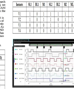
The result of transient analysis for duration of 20 ns is given in the Figure-8. Where WL is write enable signal, PRE-pre-charge, SB1-search bits for SEG_1 and SB2-search bits for SEG_2 and ML is the match line. ML goes to the logic level zero only when both SEG_1 and SEG_2 are matched. The logic values at different instants from the waveform id listed in the table 5. Here nodes V3 and V4 shows perfect match.
Table-6. Logic values of nodes at different instants.
[image:5.612.276.530.373.679.2]CONCLUSIONS
Thus high performance and low power Hybrid-CAM is designed and implemented using SOI-MOSFET. Because the CAM cells are implemented using SOI MOSFET, there is tremendous reduction in power without affecting the performance of the design. So CAM using SOI is preferred where power low and high performance application is required.
REFERENCES
[1] L. Chisvin and R.J. Duckworth. 1989. “Content addrressable and associative memory: alternative to ubiquitous RAM,” IEEE computer, Vol. 22, No.7,pp. 51-64.
[2] K. E. Grosspeitsch. 1992. “Asociative memories and processors: a survey,” IEEE Micro, Vol. 12, No.3, pp. 12-19.
[3] A.J.McAuley and P. Francis. 1991. “Fast routing table look up using CAMs”, in Proc. IEEE INFOCUM, Vol. 3, pp. 128-139.
[4] N. F.Huang, W.E. Chen, J.Y. Luo and J.M Chen. 2001. “Design of multi-field, IPv6 packet classifiers using ternary CAMs” In Proc, IEEE GLOBECOM, Vol.3, pp.1877-1881.
[5] Satendra Kumar Maurya and Lawrence T. ClarkK. 2011. “A Dynamic Longest Prefix Matching content addrressable memory for IP routing”, IEEE transaction on very large scale integration, Vol. 19, No.6.
[6] Hung-Yu Li,Chia-Cheng Chen,Jnn-shyan Wang and Chingwei Yen. 2006. “An AND-type Match line scheme for high performance Energy-efficient Content addressable memories”, IEEE Journal of solid state circuits, Vol.41, No. 5.
[7] Kostas Pagiamtzis and Ali sheikholeslami. 2006. “Content-Addressable memory (CAM)circuts and architectures: A tutorial and survey”, IEEE journal of solid state circuits, Vol. 41, No. 3.
[8] Byung-Do Yang, Yong-kyu Lee and Hyeong-Ju Kang. 2011. “a low power Content Addressable Memory using low swing search Lines”, IEEE transaction on circuits and system-I:regular paper, Vol.58, No.12.
[9] M-C. Jeng, P. M. Lee, M. M. Kuo and C.hu. “Theory, algorithm and user guide of BSIM and SCALP”.
[10]Vishwas Jaju and Vikram Dalal. 2004. “Silicon on Insulator Technology”, EE530, Advances in MOSFETs, Spring.
[11]http://www.device.eecs.berkeley.edu/bsim/?page=BSI MSOI.