GER-16422
Reference Manual
NOVEMBER
1977
NOTICE
This document contains material generated by Goodyear Aerospace Corporation and is transmitted for the purpose of aiding the transaction of business between Goodyear Aerospace Corporation and the recipient. It is understood that the material contained herein will not be used, copied, or disclosed to others, without the specific written consent of Goodyear Aerospace Corporation.
The STARAN-E Computer System continues to be improved and expanded. Interested parties should contact Goodyear Aerospace Corporation, Digital Systems Marketing, Akron, Ohio 44315; or telephone (216) 794-3631 for information regarding the latest update of STARAN-E software.
CHAPTER
1
TABLE OF CONTENTS
TITLE PAGE
FOREWORD . . . e l l . " • • • • • • • • • • • • • • • 1-9
STARAN-E ARCHITECTURE •••••••••••••••••••••••••••••••••••••••••••••• 1-1
SECTION I. INTRODUCTION ••••••••••••••••••••••••••••••••••••••••••• 1-2
G ENERA1., ••••••••••••••••••••••••••••••••••••••••••••••••••••••• 1-2 MEMO RY • • • • • • • • • • • • • • • • •••••••••••••••••••••••••••••••• 0 • • • • • • • 1-2
ASSOCIATIVE PROCESSOR CONTROL MEMORY ••••••••••••••••••••• 1-2 11I>A l1EMORY ••••••••••••••••••••••••••••••••••••••••••••••• 1-2 CONTROL ••••••••••••••••••••••••••••••••••••••••••••••••••••••• 1-4 ASSOCIATIVE PROCESSOR CONTROL •••••••••••••••••••••••••••• 1-4 MULTIPLEXED INPUT/OUTPUT CONTROL ••••••••••••••••••••••••• 1-4 PROGRAM PAGER •••••••••••••••••••••••••••••••••••••••••••• 1-5 SEQUENTIAL CONTROL ••••••••••••••••••••••••••••••••••••••• 1-5 EXTERNAL FUNCTION CONTROL •••••••••••••••••••••••••••••••• 1-5 INPUT/OUTPUT •••••••••••••••••••••••••••••••••••••••••••••••••• 1-6
SECTION II. ASSOCIATIVE PROCESSOR CONTROL ••••••••••••••••••••••••• 1-7
AP CONTROL MEMORY ••••••••••••••••••••••••••••••••••••••••••••• 1-7 GENERA1., ••••••••••••••••••••••••••••••••••.•••••••••••••• ~ • 1-7 PAGE MEMORIES •••••••••••••••••••••••••••••••••••••••••••• 1-8 HIGH SPEED DATA BUFFER ••••••••••••••••••••••••••••••••••• 1-8
MAIN M~ORY •••••••••••••••••••••••••••••••••••••••••••••• 1-9
DIRECT MEMORY ACCESS ••••••••••••••••••••••••••••••••••••• 1-9
ADDRESSING ••••••••••••••••••••••••••••••••••••••••••••••• 1-10
General ••••••••••••••••••••••••••••••••••••••••••••• l-10 Main Memory ••••••• ' •••••••••••••••••••••••••••••••••• 1-10 Page Memories ••••••••••••••••••••••••••••••••••••••• l-ll
High Speed Data Buffer •••••••••••••••••••••••••••••• 1-11 Direct Memory Access •••••••••••••••••••••••••••••••• l-l1
PROGRAM CONTROL •••••••••••••••••••••••••••••••••••••••••• 1-14 Progr am Counter ••••••••••••••••• ' •••••••••••••••••••• 1-14 Start Loop Marker ••••••••••••••••••••••••••••••••••• 1-14 End Loop Marker ••••••••••••••••••••••••••••••••••••• 1-14 Comparator •••••••••••••••••••••••••••••••••••••••••• 1-14 Program Status Register ••••••••••••••••••••••••••••• 1-14 Bus Logic ••••••••••••••••••••••••••••••••••••••••••• 1-15 BLOCK TRANSFER CONTROL ••••••••••••••••••••••••••••••••••• 1-15 Data Pointer Register ••••••••••••••••••••••••••••••• 1-15 Block Length Counter •••••••••••••••••••••••••••••••• 1-15 COMMON REGISTER •••••••••••••••••••••••••••••••••••••••••• 1-15 FIELD POINTERS AND LENGTH COUNTERS ••••••••••••••••••••••• 1-16 Field Pointer 1 ••••••••••••••••••••••••••••••••••••• 1-16 Field Pointer 2 ••••••••••••••••••••••••••••••••••••• 1-16 Field Pointer 3 ••••••••••••••••••••••••••••••••••••• 1-17 Field Pointer E ••••••••••••••••••••••••••••••••••••• 1-17 Field Length Counter 1 •••••••••••••••••••••••••••••• 1-17 Field Length Counter 2 •••••••••••••••••••••••••••••• 1-17 RESPONSE STORE CONTROL ••••••••••••••••••••••••••••••••••• 1-17 Control Line Conditioner •••••••••••••••••••••••••••• 1-18 Control Line Buffer ••••••••••••••••••••••••••••••••• 1-18 MDA ARRAY CONTROL •••••••••••••••••••••••••••••••••••••••• 1-18 Array Select Register ••••••••••••••••••••••••••••••• 1-18 Array Access •••••••••••••••••••••••••••••••••••••••• 1-18 Array Address Mode •••••••••••••••••••••••••••••••••• l-19 GENERAL REGISTERS •••••••••••••••••••••••••••••••••••••••• 1-19 RO-R7 ••••••••••••••••••••••••••••••••••••••••••••••• 1-19
R8, RB-RF ••••••••••••••••••••••••••••••••••••••••••• 1-19
2
SECTION III. PROGRAM PAGER •••••••••••••••••••••••••••••••••••••••• 1-27
GENERAl.. ••••••••••••••••••••••••••••••••••••••• 0 • • • • • • • • • • • • • • • 1-27 OPERATION •••••••••••••••••••••• It • • • • • • • • • • • • • • • • • • • • • • • • • • • • • • 1-28
SECTION IV. EXTERNAL FUNCTION CONTROL ••••••••••••••••••••••••••••• 1-30
GENERAL ••••••••••••••••••••••••••••••••••••••••••••••••••••••• 1-30
PAGE MEMORY PORT SWITCHES ••••••••••••••••••••••••••••••••••••• 1-30
INTERLOCKS •••••••••••••••••••••••••••••••••••••••••••••••••••• 1-31
PROGRAM PAGER FUNCTIONS ••••••••••••••••••••••••••••••••••••••• 1-31 ERROR CONTROL FUNCTIONS ••••••••••••••••••••••••••••••••••••••• 1-32 ASSOCIATIVE PROCESSOR CONTROL INTERRUPTS •••••••••••••••••••••• 1-32 SEQUENTIAL PROCESSOR CONTROL INTERRUPTS ••••••••••••••••••••••• 1-32 AP CONTROL ACTIVITY ••••••••••••••••••••••••••••••••••••••••••• 1-33 AP CONTROL LOOP INDICATOR ••••••••••••••••••••••••••••••••••••• 1-34 RESETS AND CLEARS ••••••••••••••••••••••••••••••••••••••••••••• 1-34
SECTION V. SEQUENTIAL CONTROL ••••••••••••••••••••••••••••••••••••• 1-35
GENER.AL ••••••••••••••••••••••••••••••••••••••••••••••••••••••• 1-35
SEQUENTIAL PROCESSOR ARCHITECTURE ••••••••••••••••••••••••••••• 1-35 SEQUENTIAL CONTROL INTERFACE •••••••••••••••••••••••••••••••••• 1-37
GENERAI.. •••••••••••••••••••••••••••••••••••••••••••••••••• 1-37
DIRECT ACCESS TO AP CONTROL MEMORY ••••••••••••••••••••••• 1-37 REGISTER READOUT ••••••••••••••••••••••••••••••••••••••••• 1-38 EXTERNAL FUNCTIONS ••••••••••••••••••••••••••••••••••••••• 1-42 INTERRUPT ACCEPTANCE ••••••••••••••••••••••••••••••••••••• 1-42 PERIPHERALS •••••••••••••••••••••••••••••••••••••••••••••• 1-42 OPTIONAL PERIPHERALS ••••••••••••••••••••••••••••••••••••• 1-43
STARAN-E INSTRUCTION SET ••••••••••••••••••••••••••••••••••••••••••• 2-1
SECTION I. GENER.AL •••••••••••••••••••••••••••••••••••••••••••••••• 2-2
PROGRAM SEQUENCE •••••••••••••••••••••••••••••••••••••••••••••• 2-2 PROGRAM COUNTER ••••••••••••••••••••••••••••••••••••••••••••••• 2-2 INSTRUCTION LENGTH •••••••••••••••••••••••••••••••••••••••••••• 2-2 INSTRUCTION TYPES ••••••••••••••••••••••••••••••••••••••••••••• 2-2
SECTION II. STARAN AP CONTROL INSTRUCTIONS •••••••••••••••••••••••• 2-3
GENERAL ••••••••••••••••••••••••••••••••••••••••••••••••••••••• 2-3
SPEED-UP CODE •••••••••••••••••••••••••••••••••••••••••••• 2-3 RULE FOR SPEED-UP MODE ••••••••••••••••••••••••••••••••••• 2-3 MDA ARRAY INSTRUCTIONS •••••••••••••••••••••••••••••••••••••••• 2-5 ARRAY SELECTION •••••••••••••••••••••••••••••••••••••••••• 2-5 MDA FLIP NETWORK ••••••••••••••••••••••••••••••••••••••••• 2-5 MIXED MODE ACCESS •••••••••••••••••••••••••••••••••••••••• 2-B LOGIC FUNCTIONS •••••••••••••••••••••••••••••••••••••••••• 2-13
SHIFTING ••••••••••••••••••••••••••••••••••••••••••••••••• 2-15 MIRRORING •••••••••••••••••••••••••••••••••••••••••••••••• 2-15 LEFT SHIFT ••••••••••••••••••••••••••••••••••••••••••••••• 2-15
INPUT SOURCE ••••••••••••••••••••••••••••••••••••••••••••• 2-15 DESTINATION OR RESULT OF AN MDA INSTRUCTION •••••••••••••• 2-17 MDA ARRAY OPERATIONS ••••••••••••••••••••••••••••••••••••• 2-1B Load X and/or Y ••••••••••••••••••••••••••••••••••••• 2-1B Load M (MASK} ••••••••••••••••••••••••••••••••••••••• 2-1B Store X, Y, or M to MDA Array Memory •••••••••••••••• 2-1B Store X or Y to MDA Array Memory Through a Mask ••••• 2-1B Load Common Register •••••••••••••••••••••••••••••••• 2-19 Resolve Operation ••••••••••••••••••••••••••••••••••• 2-19 GENERAL MDA INSTRUCTION •••••••••••••••••••••••••••••••••• 2-20 MDA INSTRUCTION FORMAT (DIRECT ADDRESS MODE} ••••••••••••• 2-25 MDA INSTRUCTION FOIDiAT (INDIRECT ADDRESS MODE) ••••••••••• 2-2B MDA INSTRUCTION FORMAT (LINK POINTER MODE) ••••••••••••••• 2-31 ALTERNATE MDA INSTRUCTION FORMAT ••••••••••••••••••••••••• 2-34 EXECUTION CONTROL INSTRUCTIONS •••••••••••••••••••••••••••••••• 2-35 BRANCH INSTRUCTION ••••••••••••••••••••••••••••••••••••••• 2-35 UNCONDITIONAL BRANCH INSTRUCTION ••••••••••••••••••••••••• 2-35 CONDITIONAL BRANCH INSTRUCTION ••••••••••••••••••••••••••• 2-36 BRANCH AND LINK INSTRUCTION •••••••••••••••••••••••••••••• 2-3B CALL SUBROUTINE INSTRUCTION •••••••••••••••••••••••••••••• 2-40 LOOP INSTRUCTION ••••••••••••••••••••••••••••••••••••••••• 2-42 LOAD AND LOOP INSTRUCTION •••••••••••••••••••••••••••••••• 2-43 AP CONTROL REGISTER INSTRUCTIONS •••••••••••••••••••••••••••••• 2-44 AP CONTROL REGISTER LOAD OPERATIONS •••••••••••••••••••••• 2-44 LEFT SHIFT ••••••••••••••••••••••••••••••••••••••••••••••• 2-45 EFFECTIVE ADDRESS FORMATION •••••••••••••••••••••••••••••• 2-46 LOAD OOfEDIATE ••••••••••••••••••••••••••••••••••••••••••• 2-47 LOAD AP CONTROL REGISTER FROM CONTROL MEMORY ••••••••••••• 2-52 LOAD AP CONTROL REGISTER FROH AP CONTROL REGISTER •••••••• 2-60 STORE AP CONTROL REGISTER TO CONTROL MEMORY •••••••••••••• 2-64
SWAP PSW ••••••••••••••••••••••••••••••••••••••••••••••••• 2-67
MOVE GENERAL REGISTER OR CONTROL MEMORY TO GENERAL
REGISTER OR CONTROL MEMORY •••••••••••••••••••••••••• 2-73 LOAD GENERAL REGISTER FROM CONTROL MEMORY •••••••••••••••• 2-75 STORE GENERAL REGISTER TO CONTROL MEMORY ••••••••••••••••• 2-77
SECTION III. PROGRAM PAGER INSTRUCTIONS ••••••••••••••••••••••••••• 2-78
GENERAL. e • • • • • • • • • • • • • • • • • • • (} • • • • • • OJ • • • • • • • • • • • • • • • • • • • • • • • • • • 2-78
PROGRAM SEQUENCE ••••••••••••••••••••••••••••••••••••••••• 2-78 INSTRUCTION LENGTH ••••••••••••••••••••••••••••••••••••••• 2-78 INSTRUCTION TYPES •••••••••••••••••••••••••••••••••••••••• 2-78 PAGER INSTRUCTIONS •••••••••••••••••••••••••••••••••••••••••••• 2-79 LOAD PUT ••••••••••• tit • • • • • • • • • • • • • • • • • • • • • • • • • • • • • • • • • • • • • 2-79 MOVE DATA •••••••••••••••••••••••••••••••••••••••••••••••• 2-80 LOAD PUT AND MOVE DATA ••••••••••••••••••••••••••••••••••• 2-81
ISSUE EXF . . . ., •••••••••••••••• 2-82
PAGER COMMAND SUMMARY ••••••••••••••••••••••••••••••••••••••••• 2-83
SECTION IV. EXTERNAL FUNCTION INSTRUCTIONS •••••••••••••••••••••••• 2-84
GENERAL •••••••••••••••••••••••••••••••••••••••••••••••••••••• • 2-84
FUNCTION CODE CLASSES •••••••••••••••••••••••••••••••••••• 2-84 INSTRUCTION FORMATS •••••••••••••••••••••••••••••••••••••• 2-84 Instruction Format From AP Control •••••••••••••••••• 2-84 Instruction Format From Program Pager ••••••••••••••• 2-84 EXTERNAL FUNCTION CODES ••••••••••••••••••••••••••••••••••••••• 2-85 PAGER PORT SWITCH INSTRUCTION •••••••••••••••••••••••••••• 2-85
INTERLOCKS ••••••••••••••••••••••••••••••••••••••••••••••• 2-87
PAGER STATE INSTRUCTION •••••••••••••••••••••••••••••••••• 2-89 PAGER LOAD GET INSTRUCTION ••••••••••••••••••••••••••••••• 2-91 ASSOCIATIVE PROCESSOR CONTROL INTERRUPTS ••••••••••••••••• 2-92 '
3
APPENDIX
A
B
C
INPUT/OUTPUT OPTIONS ••••••••••••••••••••••••••••••••••••••••••••••• 3-1
GENE~ •••••••••••••••••••••••••••••••••••••••••••••••••••••• • 3-2
DIRECT MEMORY ACCESS CHANNEL •••••••••••••••••••••••••••••••••• 3-2 BUFFERED INPUT/OUTPUT CHANNEL ••••••••••••••••••••••••••••••••• 3-3 EXTERNAL FUNCTION CHANNEL ••••••••••••••••••••••••••••••••••••• 3-4
GENERAL •••••••••••••••••••••••••••••••••••••••••••••••••• 3-4
HOST COHPUTER EXTERNAL FUNCTION INTERFACE •••••••••••••••• 3-4 BUFFERED INPUT/OUTPUT EXTERNAL FUNCTIONS ••••••••••••••••• 3-5 PARALLEL INPUT/OUTPUT EXTERNAL FUNCTIONS ••••••••••••••••• 3-5 STARAN COMMAND CHANNEL •••••••••••••••••••••••••••••••••••••••• 3-5 PARALLEL INPUT/OUTPUT CHANNEL ••••••••••••••••••••••••••••••••• 3-5
GENERAL •••••••••••••••••••••••••••••••••••••••••••••••••• 3-5
INTER-ARRAY DATA COMMUNICATION ••••••••••••••••••••••••••• 3-6 HIGH BANDWIDTH 1/0 ••••••••••••••••••••••••••••••••••••••• 3-6
INDEX •••••••••••••••••••••••••••••••••••••••••••••••••••••••••••••• X-I
TITLE PAGE
GLOSSARY OF TE~lS AND ABBREVIATIONS •••••••••••••••••••••••••••••••• A-1
INSTRUCTION SUMMARY IN HEX CODE ORDER •••••••••••••••••••••••••••••• B-l
FIGURE
1-1
1-2
1-3
1-4
1-5
2-1
LIST OF FIGURES
TITLE PAGE
STARAN-E Block Diagram •••••••••••••••••••••••••••••••••••••••••••• ~l-3
AP Control Memory Map •••••••••••••••••••••••••••••••••••••••••••••• 1-7
Base Register Format ••••••••••••••••••••••••••••••••••••••••••••••• 1-19
STARAN Register Map •••••••••••••••••••••••••••••••••••••••••••••••• 1-21
Program Pager Block Diagram •••••••••••••••••••••••••••••••••••••••• 1-28
TABLE
1-1
1-2
1-3
1-4
1-5
2-1
2-2
2-3
2-4
2-5
2-6
2-7
2-8
2-9
2-10
2-11
2-12
2-13
LIST OF TABLES
TITLE PAGE
AP Control Memory Characteristics •••••••••••••••••••••••••••••••••• 1-12
Array Base Register Selection •••••••••••••••••••••••••••••••••••••• 1-20
Access Modes ••••••••••••••••••••••••••••••••••••••••••••••••••••••• 1-24
Sequential Control Interrupt Vector Addresses •••••••••••••••••••••• 1-33
Sequential Control Readout Registers ••••••••••••••••••••••••••••••• 1-39
Logic Table •••••••••••••••••••••••••••••••••••••••••••••••••••••••• 2-14
Shift Table •••••••••••••••••••••••••••••••••••••••••••••••••••••••• 2-16
Associative Processor Control Register Abbreviations ••••••••••••••• 2-45
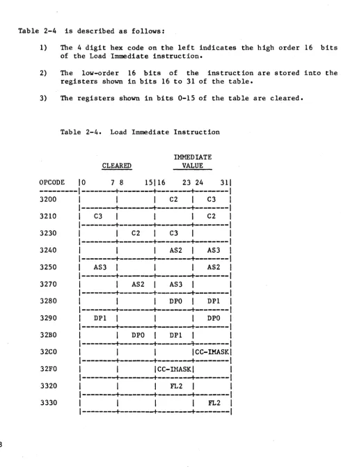
Load Immediate Instruction ••••••••••••••••••••••••••••••••••••••••• 2-48
Load Register from Control Memory •••••••••••••••••••••••••••••••••• 2-54
Load AP Register from Register Source Options •••••••••••••••••••••• 2-62
Load AP Register from Register Destination Options ••••••••••••••••• 2-63
Store AP Register to Control Memory Source Options ••••••••••••••••• 2-66
Pager EXF Functions •••••••••••••••••••••••••••••••••••••••••••••••• 2-82
Summary of Pager Commands •••••••••••••••••••••••••••••••••••••••••• 2-83
Summary of Pager Port Switch EXF Instructions •••••••••••••••••••••• 2-86
Summary of Interlock EXF Instructions •••••••••••••••••••••••••••••• 2-88
FOREWORD
STARAN COMPUTER SYSTEN GENERAL DESCRIPTION
FEATURES
MDA ARRAYS
STARAN, a new and unique architecture for computer systems, is the result of over a decade of intensive development effort in associative and parallel processing at Goodyear Aerospace. STARAN, the first associative processor (AP) to go into production, can operate independently or in a hybrid system to complement a conventional computer (host computer).
The STARAN approach to parallel processing is rather general and is based on the cooperative interconnection and control of three basic system components:
(1) A Multi-Dimensional Access (MDA) memory (2) A set of processing elements (PE's)
(3) A communications network connecting the MDA to the PE's and both of these to other devices
The key component of the STARAN computer system is the lIDA array memory, which provides content addressability and parallel processing
capabilities.
ASSOCIATIVE PROCESSOR CONTROL
The AP control performs data manipulations within the MDA arrays as directed by instructions stored in AP control memory.
ASSOCIATIVE PROCESSOR CONTROL MEMORY
•
AP control memory contains high speed page memories and a High Speed Data Buffer (HSDB) to provide fast access to data and instructions that require frequent access and/or fast execution.
AP control memory also contains a main memory for program storage.
A basic STA~l Control Memory consists of:
(1) Three page memories, each containing 4096 32-bit words (2) One HSDB containing 512 32-bit words
(3) A main memory containing up to 32,768 32-bit words
(4) Any addresses not used for main and HSDB memory are reserved for DMA
PROGRAM PAGER
The program pager moves program segments, which require fast execution, from main to the page memories.
SEQUENTIAL CONTROLLER AND MEMORY
The Sequential Controller (SC) provides offline capabilities for assembling and debugging STARAN programs, a communication link between STARAN and the operator, and control for diagnostic and test programs.
The basic system contains 16,384 16-bit words of sequential control memory.
EXTERNAL FUNCTION LOGIC
External function logic enables an element of STARAN to control, and interrogate the status of other elements. An external function code may be issued by AP control, the program pager, sequential control, and the host computer.
INPUT/OUTPUT
The following input/output variations are provided on the STARAN system:
(1) Direct Memory Access to a host computer
(2) An input/output channel 32 bits wide to STARAN control memory (BIO)
(3) External Function channel 'to pass function codes between the STARAN control elements
(4) MUltiplexed Input/Output unit (MID) providing: (a) Continuous transmit mode
PHYSICAL DESCRIPTION
CHAPTER 1
GENERAL
HEMORY
SECTION I. INTRODUCTION
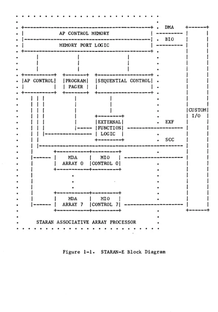
The STARAN-E system introduces a new concept in computers, designed to achieve very high processing rates economically. Figure 1-1 shows a block diagram of the STARAN-E computer. Each block of the diagram is discussed briefly in the following paragraphs. More detailed discussions are presented in subsequent areas of this manual.
STARAN-E consists of two separate memory organizations: the AP control memory, essentially a program memory, and the Multi-Dimensional Access
(MDA) array memory, a data memory.
ASSOCIATIVE PROCESSOR CONTROL MEMORY
The main function of the Associative Processor (AP) control memory is to contain assembled AP application programs. The control memory can also contain items of data and act as a buffer between AP control and other elements of STANAN-E. The AP control memory consists of up to 16 memory blocks. Each block contains 4096 32 bit words. Some memory blocks are fast to enable AP control to fetch its instructions rapidly (page memories and the High Speed Data Buffer); others are slower to economically contain the entire control program (main memory).
MDA ARRAY HEHORY
·
.
. . .
. .
.
.
.
.
.
.
.
.
.
.
.
.
.
.
.
.
· +---+.
DMA+---+
• I AP CONTROL MEMORY I---· 1---1 ---·
BIO • I MEMORY PORT LOGIC I---· +---+ .
· +---+ +---+ +---+ .
• lAP CONTROL
I I
PROGRAM I ISEQUENTIAL CONTROLI •
• I
I
I PAGER I 1 I •· +---+ +---+ +---+.
I I
I
I
I I 1 I
I I
I
I CUSTOM1 J I
+---+
I/OI I 1 1 EXTERNAL I • EXF
I I
1--- 1
FUNCTIONI
---I 1--- ---I
LOGICI
+---+.
SCC1---+---+---+
.
--- 1 MDA I MIO 1
---1 ARRAY 0 ICONTROL
01
+---+---+
+---+---+
I MDA 1 MIO I
--- / ARRAY 7 /CONTROL 71
---+---+---+
+---+
STARAN ASSOCIATIVE ARRAY PROCESSOR
. . . .
.
. .
.
. .
.
.
.
.
. .
[image:18.617.74.521.104.742.2]CONTROL
The basic STARAN-E array module consists of a set of processing elements connected to a high bandwidth MDA memory through a permutation network. Rows, columns, or other subsets of data can be read in parallel from the memory, permuted in various ways in the permutation network, and combined with other data in the processing elements. Processed results can also be permuted and stored into memory in various ways.
Each MDA array contains 256 words, each word having a minimum of 1024 bits with up to 65,536 bits optional. Each array also contains 256 processing elements. Initially, one can think of each of the 256 PE's as being connected to one of the 256 MDA words, each PE thus having its own local 1K to 64K (K-1024) bit memory with data being transferred between PE's and memory via the flip network. However, to view each PE as being connected to its own word is needlessly restrictive. Any of the 256 PE's within an array can have access to any bit of MDA storage within that array.
The STARAN-E consists of 5 processing elements: AP control, multiplexed I/O control, program pager, sequential control, and the external function control which provides control and communication between the other four processing elements.
ASSOCIATIVE PROCESSOR CONTROL
AP control is directly responsible for manipulation of data within the MDA arrays under control of the program contained within the AP memory. Associative operations are coordinated and controlled by AP control.
MULTIPLEXED INPUT/OUTPUT CONTROL
Inter-array communication and input/output between arrays and external devices is controlled by the Multiplexed Input/Output Unit. There are
PROGRAM PAGER
(b) Block transfer mode will transfer a block of data from one array to another.
(c) Exchange transfer mode is extremely flexible in that data from an array can be transferred to any and/or all of the other arrays. The only restriction is that a particular array can receive data from only one source. However, data from a particular array may be transferred to any number of other arrays. Any operation using the normal MDA instruction format can be executed in the exchange transfer mode.
The program pager speed main memory of transfer functions control is executing pager can be loading
loads the high-speed page memories from the lower AP control memory. The pager performs these independently of AP control, so that while AP a program segment out of one page memory, the another page memory with a future program segment.
SEQUENTIAL CONTROL
The sequential control portion of STARAN-E consists of a sequential processor (SP) having a 16k memory, a keyboard/printer, a disk drive, a paper tape reader/punch, and logic capability to interface the sequential processor with other STARAN-E elements. Sequential control is used for system software programs such as assembler, operating system, diagnostic programs, debugging, and housekeeping routines.
EXTERNAL FUNCTION CONTROL
INPUT/OUTPUT
STARAN-E has a variety of input/output (I/O) options available. A custom I/O cabinet can be obtained as part of the basic STARAN-E system. STARAN-E can also be integrated with a variety of other computer systems. A Direct Memory Access (DMA) channel to a host-computer enables a rapid interchange of data between the systems.
An I/O channel (BIO) provides access to STARAN control memory, and an external function channel permits interrupts and/or other control information to be passed between the two systems. THE STARAN Command Channel (SeC) provides a means for STARAN to control and sense external peripheral devices.
SECTION II. ASSOCIATIVE PROCESSOR CONTROL
AP CONTROL MEMORY
GENERAL
The main function of the AP control memory is to contain the assembled AP application programs. AP control memory can also be used for data storage and as a buffer between AP control and other elements of STARAN-E. Since the AP control memory is not an integral part of the MDA array memory, AP control can overlap the AP control memory cycle with the MDA cycle time.
AP control memory is divided into several memory blocks (see Figure 1-2). Three fast memory blocks, called pages, contain the current (active) AP program segments; the slower main memory blocks contain the remainder of the AP program. A program pager is included in STARAN-E to facilitate transfer from the slow to the fast memory blocks.
Each word of AP control memory instructions. The exception to this contain instructions only, not (most-significant) bit, and bit 31 is of each word. Each word is given hexadecimal notation.
contains rule is
data. the right a 16-bit
32 bits of either data or page memory, which can Bit 0 is the left (least-significant) bit address expressed in
o
8000 8200 DODO EOOO FOOO+---+---+---+---+---+---+
I
I
I
I
I
I
I
I
I
I
I
PAGEDI
PAGElI
PAGE2I
I
I
I
DMAI
I
I
I
I.
MAINI
HSBDI
SHAREDI
I
I
I
I
MEMORYI
I
HOST r 4096I
4096I
4096I
I
I
I
STORAGEI
WORDSI
WORDSI
WORDSI
I
I
I
I
I
I
I
+---+---+---+---+---+---+
PAGE MEMORIES
Three page memories are included in the AP control memory: Page 0, Page 1, and Page 2. Page memories use fast, bipolar, solid-state elements that are volatile. Each page contains 4096 words in the basic STARAN-E configuration. The page memories can be doubled to 8192 words each on an optional basis.
Page 0 may contain a library of routines that require fast execution, such as arithmetic subroutines. Pages 1 and 2 can be used in ping-pong fashion, with the AP control executing instructions out of one page while the other is being loaded by the program pager. This permits the programmer to use the faster memory for certain segments of the program or the entire program if fast execution is required.
Each page memory has a port switch that connects it to one of three buses. The port switch is controlled by external function codes. At any given time, a page memory is connected to 1) the instruction bus, which allows AP control to read instructions from the page; 2) the pager bus, which allows the program pager to load the page; or 3) the sequential control bus, which allows sequential control to read items from the page. If one of these buses should try to access a word in the page memory while the port is set to another bus, a hangup results. Hangups, which are sensed by error detectors, cause an interrupt in sequential control.
HIGH SPEED DATA BUFFER
A port priority switch on the HSDB resolves any conflict among buses. Each memory cycle is given to the highest priority bus requesting an HSDB address at that time, while other buses requesting HSDB addresses wait for the next memory cycle. Priorities among buses are as follows:
1) An I/O bus to I/O cabinet (highest priority)
2) Sequential control bus
3) AP control instruction bus
4) Program pager bus
5) AP control data bus (lowest priority)
MAIN MEMORY
The main memory uses configuration it contains through 7FFF).
nonvolatile core storage. 32,768 words (hexadecimal
In the addresses
basic 0000
Like the High Speed Data Buffer (HSDB), the main memory is accessible to all buses that can access AP control memory (through a priority port switch that gives each memory cycle to the highest priority bus requesting a main memory address). The priorities of the buses are the same as those for the High Speed Data Buffer.
The main memory is used to contain the AP control programs. Because the main memory is slower than the page memories, it is recommended that program segments be moved into the page memories for execution. Also, since the main memory is accessible to all buses having access to AP control memory, it is also useful as a buffer for data.
DIRECT MEMORY ACCESS
All buses accessing AP control memory can access the DMA block. A priority port switch "resolves any interbus conflicts, giving each access cycle to the highest priority bus requesting a DMA address at the time. Priorities among buses are the same as those for the High Speed Data Buffer.
ADDRESSING
General
Each AP control memory word contains 32 bits of either data or instructions. Each word is given a 16-bit address.
Main Memory
The main memory contains 32,768 words of memory configuration. These words are assigned hexadecimal through 7FFF.
in the addresses
basic
0000
Certain For the follows:
words basic
in the main memory are dedicated to special purposes. configuration of STARAN-E, these locations are as
Hexadecimal Address Dedicated Usage
0000
0001
OOOF
First AP control instruction when activated AP control interrupt 1
AP control interrupt 15
Page Memories
The three page memories, 4096 words each, that are included in the AP control memory are designated Page 0, Page 1, and Page 2. In the basic configuration, Page 0 contains hexadecimal addresses DOOO through DFFF; Page 1 contains hexadecimal addresses EOOO through EFFF; and Page 2 contains hexadecimal addresses FOOO through FFFF.
High Speed Data Buffer
The High Speed Data Buffer contains 512 words of memory in the standard configuration, but can be doubled to 1024 words on an optional basis. In the basic configuration, the High Speed Data Buffer contains hexadecimal addresses 8000 through 81FF.
Direct Memory Access
A block of AP control memory addresses is reserved for the Direct Memory Access (DMA) channel to access the memory of a host computer. This block can contain up to 20,480 addresses which are assigned hexadecimal addresses 8200 through CFFF. This block can be reduced if page memories or the High Speed Data Buffer is increased in size.
AP CONTROL MEMORY SUM~~RY
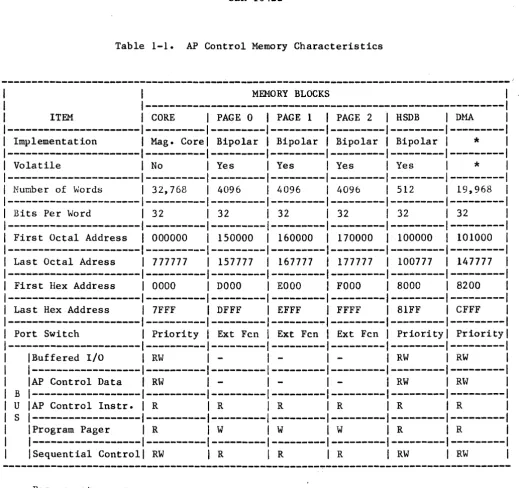
Table 1-1. AP Control Memory Characteristics
---~---~---~---~---)
I
MEMORY BLOCKSI
1---1
ITEM I CORE I PAGE 0 I PAGE 1 I PAGE 2 I HSDB I DMA I
---1---1---1---1--- ---1---1
Implementation I Mag. Corel Bipolar 1 Bipolar I Bipolar Bipolar I
*
I---1---1---1--- --- ---1---1
Volatile I No 1 Yes I Yes Yes Yes I
*
1---1---1---1--- --- ---1---1
Number of Words
1
32,7681
40961
4096 4096 5121
19,9681
---1---1---1--- --- ---1---1
Bits Per \.Jord
1
321
321
32 32 321
321
---1---1---1--- --- ---1---1
First Octal Address I 000000 I 150000 I 160000 170000 100000 1 101000 1
---1---1---1--- --- ---1---1
Last Octal Adress I 777777 I 157777 I 167777 177777 100777 I 147777 I
---1---1---1--- ---1---1---1
First Hex Address I 0000 1 DOOO I EOOO FOOO I 8000 I 8200 I
---1---1---1---1---1---1---1
Last Hex Address 1 7FFF 1 DFFF I EFFF I FFFF I 81FF I CFFF 1
---1---1---1---1---1---1---1
Port Switch 1 Priority 1 Ext Fcn I Ext Fcn 1 Ext Fcn 1 Priority 1 Priority I
---1---1---1---1---1---1---1
IBuffered I/O 1 RW I - 1 - I - 1 RW I RW 1
1---1---1---1---1---1---1---1
I AP Control Da ta I R\.J 1 - I - I - I RW I Rt-l I
B
1---1---1---1---1---1---1---1
U lAP Control Instr. I R I R I R I R I R I R 1
S
1---1---1---1---1---1---1---1
1 Program Pager 1 R I W 1
w
Iw
I R I R I1---1---1---1---1---1---1---1
I Sequential Control I RW I R I R I R I RW I RW I
- Bus cannot access memory
R Bus can only read from memory
W Bus can only write into memory
RW Bus can both read and write into memory
[image:27.615.36.555.96.584.2]AP EXECUTION CONTROL
GENERAL
The major function of the AP control is to control the STARAN-E ~IDA arrays. AP control fetches instructions from the AP control memory. A program counter contains the address of the instruction, while an instruction register contains the instruction itself. Some instructions perform array operations, while others perform AP control functions. AP control consists of the following elements:
1) Instruction Register 2) Program Control
3) Block Transfer Control 4) Common Register
5) Field Pointers and Length Counters 6) Response Store Control
7) Array Control 8) General Registers
INSTRUCTION REGISTER
The instruction register contains the instruction being executed. The instruction loaded into the instruction register is received from AP control memory via the instruction bus. Parity is ch.ecked at the instruction register. The instruction register contains 32 bits which are numbered from 0 to 31 with bit 0 at the left. Portions of the instruction register are used as a direct source of data or addresses as a function of the instruction being executed.
PROGRAM CONTROL
Program Counter
The Program Counter contains the address of the instruction being read
fro~ control memory. It is a 16-bit counter incremented by AP control.
The Program Counter may be loaded from the bus logic; e.g •• a branch instruction loads an address. The contents of the Program Counter-form bits 0 through 15 of the program status word.
Start Loop Narker
The Start Loop Marker is used to store the address of the first instruction immediately following a loop instruction. The Start Loop Marker is a 16-bit register loaded directly from the Program Counter at
the start of an instruction loop. It is loaded into the Program Counter when the last instruction of the loop has been executed and the loop is to be repeated.
End Loop Marker
The End Loop Marker is used to store the address of the last instruction of a loop. The End Loop Marker is a 16-bit register loaded from the rightmost 16 bits of the loop instruction.
Comparator
The Comparator compares the address contained in the end loop marker with the address in the Program Counter. The Comparator is a full 16-bit Comparator. the output of which is transmitted to control as an
indica~ion that the end of a loop has been reached. The control then
loads the Start Loop Marker contents ,into the Program Counter if the loop is to be repeated.
Bus Logic
The bus logic provides a common data path for all pertinent registers of AP control and the data bus from control memory. The bus is 32 bits wide. Registers of less than 32 bits are grouped to form a 32-bit word. Details of registers connected to the bus and register grouping are shown in Figure 1-4.
Data transmitted via the bus logic passes through the bus shift logic. The bus shift logic shifts the bus word left end around by either 0, 8, 16, or 24 bit positions. The amount of shift is controlled by the instruction moving the data. Data received from AP control memory is checked for correct parity as it passes the bus shift logic- Data stored in the control memory has an odd parity bit generated by the bus shift logic.
BLOCK TRANSFER CONTROL
Data Pointer Register
The Data Pointer register contains the control address for the data bus for block transfers. The Data Pointer is a 16-bit counter. The Data Pointer can be stepped with each transfer within a data block.
Block Length Counter
The Block Length counter, a 16-bit decrementing counter, controls the length of a data block transfer.
COID-fON REG ISTER
generator. The use of the mask allows formatting of an output word from noncontiguous data in an array.
The mask generator generates a mask pattern to be used in loading array output data into the Common register. The mask enables data to be loaded for a number of contiguous bits. The mask generator requires the bit addresses of the most and least significant bits to be loaded. All bits between and including these limits are loaded. while those outside these limits are unaltered.
FIELD POINTERS AND LENGTH COUNTERS
Field pointers generally contain bit slice or word addresses in the MDA array operations. The field length counters control the number of bits to be operated on in sequence. There are three field pointers and two field length counters. In addition. one register is used as a temporary pointer or can contain a shift code for certain array operations. A selector is used to route either field pointer 1. 2. or 3 or the address field of the instruction register to the array. These registers are 8 bits in length and their contents range from 0 to 255. When attempting to increment above 255. the register will return to zero; when attempting to decrement below zero. the register contents become 255. The field length counters can only be decremented.
Field Pointer 1
Field Pointer 1 plus base register RC specifies an array word or bit address for an MDA operation. FPl is also used to specify the address of a selected bit of the Common register to be used for a search instruction. Field Pointer 1 (like field pointers 2 and 3)is an 8-bit counter. In addition. as a result of the resolve operation. Field Pointer 1 will be loaded with the number of the array module containing the first responder (i.e., first selected word whose Y bit is set to one).
Field 'Pointer 3
Field Pointer 3 plus base register RE specifies an array bit or word address.
Field Pointer E
Field Pointer E is an 8-bit counter. It can be used for temporary storage of an array bit or word address, or it can contain a shift constant for certain 11DA operations.
Field Length Counter 1
Field Length counter 1 and Field Length counter 2 are 8-bit counters. The length counters can only be decremented. When the contents of a field counter become zero, a signal is sent to AP control for test purposes. This permits the program sequence to be altered by a branch if a field length counter becomes zero. Field Length counter 1 contains the number of cycles for a loop instruction.
Field Length Counter 2
Field Length counter 2 may be used to control the cycles of a major instruction loop, such as mUltiply fields.
RESPONSE STORE CONTROL
Control Line Conditioner
The control line conditioner generates the control signals required to manipulate the response store. These signals are generated as a function 'of the instruction register, a selected bit of the Common Register and the inclusive-OR output from the resolver.
Control Line Buffer
The control line buffer contains the control signals transmitted to the MDA arrays which allows overlapping of array instructions.
MDA ARRAY CONTROL
Control lines to the 11DA arrays not generated by the response store control are generated by the array control. The array control logic selects which arrays are to be used and controls such things as bit/word mode, store masked, and shifting.
Array Select Register
The Array Select register establishes which array modules are to be enabled for an operation. The Array Select register is 32 bits wide. Each bit position controls one array. Bit
°
corresponds to Array 0, and a 1 in a bit position enables the corresponding array. The ArraySelect register contents are also used by the resolver logic.
Array Access
Array Address Mode
The array address mode is determined by the value in the most significant 8 bits of one of the six array address base registers. Table 1-2 illustrates how a particular base register is selected.
GENERAL REGISTERS
RO-R7
There are 16 general 32-bit registers, RO through RF. Fourteen of these registers have various special uses.
Registers RO through R7 are used as index or branch and link registers. R7 is also used by the special branch and link instruction whose mnemonic is CAL.
R8, RB-RF
These six registers serve as array address base registers. Each of these registers contains a 16-bit array base address and an 8-bit storage mode. The base register format is defined in Figure 1-3.
o
I
I
MODEI
7 8 15 16
I
NOT
I
DEFINED
I
31
I
ARRAY BASE ADDRESS
I
I
Table 1-2. Array Base Register Selection
INSTRUCTION
ADDRESSING BIT BIT BIT BIT ADDRESS ADDRESS* HODE _ 5_ _7 _ _ 8_ _9 _ BASE DISPLACEHENT
DIRECT 0 0 RB 1(8-15)
INDIRECT (FPl) 0 1 0 0 RC FPl
INDIRECT (FP2) 0 1 0 1 RD FP2
INDIRECT (FP3) 0 1 1 0 RE FP3
INDIRECT (FPI2) 0 1 1 1 RF FP2
DIRECT 1 0 RB 1(8-15)
INDIRECT (FPl) 1 1 0 0 R8 FPl
INDIRECT (FP2) 1 1 0 1 R8 FP2
INDIRECT (FP3) 1 1 1 0 R8 FP3
INDIRECT (FPI2) 1 1 1 1 R8 FP2
GENERAL REGISTERS
+---+
RFI LINK PTR BASE I
+---+
REI FP3 BASE
I
+---+
RDI FP2 BASE I
+---+
RCI FP1 BASE
I
+---+
RBI DIRECT BASE I
+---+
RAI
I
+--
--+
R91
I
+---+
RBI ~IDA STACK PTR
I
+---+
R71 SYS RETURN REG I
+---+
R61 SYS STK PTR
I
+---+
R51
+
+--
--+
R41 I
+--
--+
R31 I
+--
INDEX--+
R21 I
+--
REGISTERS--+
R11
I
+--
--+
ROI I
+---+
0 31
AP CONTROL REGISTERS
+---+---+
CI
CHI
CLI
+---+---+
ASI ASH
I
ASLI
+---+---+
I
BLI
DPI
+---+---+--+--+
PSW/ PC I 0 ICCIIMI
+---+---+---+--+--+
I FL2
I
FPE I 0I
+---+---+---+---+
FI FL1 / FP3
I
FP1 I FP2I
+---+---+---+---+
o
8 16 24 31
PC Program Counter 1M Interrupt Mask
CC Arithmetic Condition Code N Negative Result Bit Z Zero Result Bit
o
Overflow Bit C Carry BitCH Common. High-half CL Common. Low-half
ASH Array Select. High-half ASL Array Select. Low-half BL Block Length
DP Data Pointer
[image:36.615.79.485.129.684.2]MDA MEMORY
GENERAL
Each STAR~l-E array consists of 256 words (rows) with an optional number of bits per word. The basic array contains two types of memory:
(1) a high speed bipolar section, and (2) a slower speed MOS section.
An .
array may consist of up to 7K bits per word of high speed memory (K=1024). The amount is variable in 1K increments. An array may contain a maximum of 64K bits per word. The slower speed MOS portion is variable in 4K increments. Associated with each word of array memory is a 3-bit processing element consisting of three I-bit MDA registers, M, X, and Y, i.e., one bit for each word of array memory. Also included in each array is a permutation (flip) network to facilitate data manipulation and interword communication, and a 256 bit wide data path to a Multiplexed Input/Output Unit. The tIDA array consists of three basic components: the array memory, the permutation (flip) network and the MDA registers. As many as 8 MDA arrays may be contained within one system. Any combination from 1 to 8 arrays may be selected and operated on concurrently.Each basic array is organized as a matrix of 256 words by 9216 bits of solid-state storage. By use of a special organization within the array, access may be made in either the bit or word direction. Consider an array as organized into square segments of 256 words by 256 bits per word. The basic array would contain 36 such segments. A word of 256 bits or a bit slice, bit n of all 256 words, of any segment may be accessed. The permutation network can shift and rearrange bits in the response store portion of the t1DA. The response store portion of the array consists of 256 response store elements. The M, X, and Y registers (256 bits each ) may be used as temporary storage of data loaded from the array or may contain the data to be stored into the array. The X and Y registers can perform logic functions on array data. The M (MASK) register is used as a mask to select which words of array memory participate in an array store operation. The Y register is used as a responder by the resolver in a search type operation. The X register is used as temporary storage when performing logic operations. The X and Y regi~ters can also perform logical functions simultaneously with the load operations.
ADDRESSING
Addressing within the MDA arrays is represented in hexadecimal notation. The four basic areas to be addressed are arrays, words, bit columns, and fields.
Arrays
Words
Addressing of arrays is accomplished by an address from 0, the first array, to
7,
the last array. The number of arrays within a system, therefore, ranges from 1 to 8 as dictated by the requirement placed on the system. The internal organization and addressing of all arrays is identical.Addressing of a word within an array is accomplished by an address from 0, the first word, to 255, the last word. The basic array word consists of 9216 bits. Any 256-bit section may be accessed in parallel or divided into eight fields of 32 bits each and accessed via the Common Register.
Bit Columns
Addressing of a bit position within an array address from 0, the most-significant least-significant (right) bit position. Bit accessed by using address (n).
Fields
is accomplished by (left), to 9216,
(n) of all words an the is
Access Mode
The array memory can be accessed horizontally, vertically or any combination thereof. Control of the access mode is via an 8-bit code. There are 256 access modes, each giving a unique mapping of .data within an array.
The most commonly used access modes are mode 0 and its complement, mode FF (255). Mode 0 is the bit-slice mode where one bit of each array word is accessed. This mode is used for mapping single bit flags and arithmetic fields. Mode FF is word mode and accesses 256 bits of one array word. Other modes are intermediate to the bit-slice and word modes since they access some bits of some words. Some useful modes are defined in Table 1-3.
Table 1-3. Access Modes
Number of Number of selected accessed
Mode Mode rows in bits in the
(Hex) (Binary) each array selected rows
00 00000000 256 1
01 00000001 128 2
03 00000011 64 4
07 00000111 32 8
OF 00001111 16 16
IF 00011111 8 32
3F 00111111 4 64
7F 01111111 2 128
FF 11111111 1 256
FE 11111110 2 128
FC 11111100 4 64
F8 11111000 8 32
FO 11110000 16 16
EO 11100000 32 8
CO 11000000 64 4
OPERATIONS·
Load
Store
The operations performed within the associative array can be grouped into the following categories: load, store, logical, resolve, and exchange.
Data loaded from the array memory can be sent to the 256-bit output bus or loaded into one of the MDA registers. By specifying a field address (section), a field (section) of one word may be loaded from the array memory for output over the 32-bit output bus to the Common register. Data is loaded from the array memory in a mode as selected by the particular base register. One MDA register may be loaded with the contents of another MDA register. All loads from the array storage are nondestructive. Logic may be performed on the X and/or Y registers simultaneously with the load operation.
Data is stored into the array memory in a mode as selected by the particular base register. Data to be stored may come from the MDA registers, the 32-bit input bus, or the 256-bit input bus (MID). The data, regardless of source, may be stored through a mask contained in l1DA register M.
Logical
Resolve
The array number and the address of the first Y register bit set is continuously resolved. This address and the inclusive-OR of all Y register elements are made available to control. This address (which is stored in FPl and FP2) may be used in succeeding operations.
Exchange
GENERAL
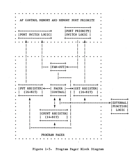
SECTION III. PROGRAM PAGER
The function of the program pager is to transfer program segments from the main memory to the page memories.
Under normal programming practice, the pager is activated by AP control when a new program segment is to be transferred to a page memory. The program pager transfers the segment one word at a time at a rate dictated by the source memory, while AP control executes instructions from previously loaded segments. When the pager completes the transfer, it restores the page memory port switch to the AP instruction bus and halts.
The program pager contains three registers (see Figure 1-5). The GET address register contains a 16-bit AP control memory address. If the pager is in the midst of moving data, the GET address points to the memory location containing the next source word to be moved. At other times the GET address register acts like a program counter, pointing to the location of the next pager instruction to be executed.
The PUT address register holds a 16-bit AP address. memory location into which the next destination word during a data move operation.
It points to the is to be put
OPERATION
·
.
.
.
. .
.
.
.
.
. . .
.
.
.
.
. .
.
. .
.
• AP CONTROL MEMORY AND MEMORY PORT PRIORITY
+---+ • +---+ IPORT PRIORITY
I
• IPORT SWITCH LOGICI ISWITCH LOGIC
I
• +---+ +---+· . . •.
•.
. . .
·1· .•. ·
I
I
I
1 I 1
I
I
I
I· · · · I· · · . .
·1· ·1· · · · ·
I I 1
I I +---+ I 1
I
1---
IFAN-OUTI~---I I1 +---+ I
1 1 I
1
1---
I
I 1 I
• +---+ +---+ I +---+ • • IpUT REGISTERI~---I PAGER I--+~IGET REGISTERI •
• 1 (16-BIT) I 1 CONTROL I I I (16-BIT) I .
• +---+ +---+ I +---+ •
• • • I . +---+
1 I I---+---+---~IEXTERNALI
I
V
I
I FUNCTIONI
I +---+ I I LOGIC I
I
ICOUNT REGISTERI I +---+I
I
(14-BIT) II
I +---+
I
I
•
I
1---+---PROGRAM PAGER
·
.
.
.
.
.
.
.
.
.
.
.
. . .
[image:43.621.75.532.107.622.2]from being "pager bound", AP programs should be segmented carefully. An ideal program segment will contain enough long instructions, subroutine calls and loops, etc., so that before AP control leaves the segment, the pager has enough time to get the next segment loaded in a page memory. If all segments are ideal, AP control will never wait for the pager.
Each page memory has a port switch to prevent AP control from starting execution in a segment before the pager has loaded it. A premature attempt to execute instructions in a page memory that is still being loaded by the pager will be delayed until the pager has switched the port switch to the instruction bus.
Pager operation is initiated by an external function code that loads the GET address register. With one external function, the current pager operation can be stopped in midstream and a new operation started. For instance, suppose from program segment 1 AP control jumps to either program segment 2 or to program segment 3, depending on some condition. Most of the time it jumps to segment 2. In this case, AP control can initiate the loading of segment 2 as it begins executing segment 1, so that little or no time is lost in waiting for the pager. In the rarer case, when AP control jumps to segment 3, it can stop loading segment 2
in midstream, if necessary, and start the loading of segment 3.