~.H~Hl-
__
-~-
______ -____
~~
__
-_~-(8) 86.09.02 (7) 86.06.03 (6) 86.04.14 (5) 86.02.25 (4) 85.07.19 O:DK512:GEN:Spc-001 (3) 85.07.10·DK512 Winchester Disk Drive
DK512
WINCHESTER DISK DR!VE
. IRE V
I
1
K
6600074
SHEET NO';."HO I fWhile every effort has been made to ensure that the information provided herein is correct please feel free to notify us in the event of an error or inconsistency.
Hitachi makes no representations or warranties with respect to the contents hereof and specifically disclanns any implied warranties or merchantability or fitness for any purpose.
Further,Hitachi reserves the right to revise this publication and to make changes from tbne to t~e in the content hereof without obligation to
.lotify any person of such revisions or changes.
Copyright Hitachi,Ltd. 1984, 1985, 1986
REVISION RECORD
CODE
AD: Addition, CH: Change, CR: Correction, DL: Deletion
Revision
Page
Section
Sub.iects
COdE
0~1 ALL
Document number
ADNarICE
Copyright
ADREVISION
Copyright
DL
2-1
2.1 Modle
85.7~86.1 120.0~120.6CR
171.4~172.4
CR
1~2 .;
Operating Brief
DL
2~3
2-4
Acess Time
25rns .... 23
CH
2-5
SEEK ERR RATE
106~107CR
4-1
Fig 4-1
20sec-=;-25sec
CR5-3
Fig 5-2
AM FOUND-N
CR
5-4
Fig 5-3
N~P CR5-6
Table 5-4
NOTESDL
5-7
Fig 5-4
T2>30 ..;.. T2>20
CH5-8
Fig 5-6,7
7 or 8
~8 or 9
CH
25
~20
CH
5-9
5.1.1.4
25
--720
CH
5-13 Table 5-13
CH
5-14 5.1.1.5(7)
CH
5-15 5.1.2.2
20
~30
CH5-16 Fig 5-14
20
~30
CH
5-17 Table 5-9
*1 add
AD5-18 Table 5-10
CH
5-19 Table 5-19
NOTES CH5-20 Table 5-20
ALLCH
5-23 5.1.2.7
BYTE 'CIDCK ADD
AD
5-24 5.1.2.7
ADDRESS MARK FDUND
AD
5-25 Fig 5-19
CH
5-26 Fig 5-20
CH
5-27 5.2.2.3
ALL AD6-1
6
20832
~20944
CH
6-6
Table 6-1
CR
6-8
6.4.1.1
CR
6-9
6.4.1.2
OPTION DEFECT LIST
AD6-13
3~4
5-d
Fig 5-6
10 BYTES Min
CH
5-9
Fig 5-9
10 BYTES Min CH6-8
Fig 6-2
F8
~FE
CH
6-9
2-(8)
CH
6-10 6.4.1(2)
CR
6-13
CR
Rev~s~on Page Sect~on
4~5 (~) TABLE OF CONTENTS
(iv) LIST OF FIGURES
2-5 TABLE 2-1
2-4 TABLE 2-1
2-11 2.13
2-12 2 .. 15
3-1 3.1
3-7 Figure 3-7
4-1 4.1
4-4 4.4
5-7 Figure 5--5A
5-13 5.1.1.5(5}
5-17 Table 5-9
6-13 6.4.2
iii TABLE OF 0JNTENrS
5~6 5-19 Table 5-11
, .
6~7 3-3 Figure 3-3
5-17 Table 5-9
7-..,.8 5-4 Figure 5-3
Table 5-2 5-18 Table 5-10
5-19 Table 5-11 5-13 Table 5-6
:
SuoJects Code
CR AD
Specification CR
Specification CH
SZl18 Read/Write PC Board CR
SZl17 Analog PC Board CR
Physical Description CR
Ground Cable D Conn. CR
DC B:>wer Requirements CH
Control Signal Transmitter CH
and Receiver Circuits
WRITE GATE TERMINATION AD
Control CH
General Configuration
rn
Response Bits
Defect Definitions DL
CH
Standard Status Response CR
Bits
DK512 Mounting Dimensions AD
General Configuration CR
Resp:>nse Bits
rata Cable C Signals CH
Pinout for rata Cable C
Specific Configuration AD
Response Bits
Standard Status Response AD
Configuration Definition AD
T A-g L E o F CON TEN T S Chapter 1. 2. 3. INTRODUCTION
• • • • • • • • • • • • • • • • • • • • • • • • • • • • • • • 0 • • 0 0 • ~
1.1 1.2 1.3 1.4
Purpose
• • • • • • • • • • • • • • • • • • • • • • • • • • • • • • • • • • • 0 e
Manufacturer ••.•.••••••.•••••...• ~ ••.•..••• Quality Control
Related Documents
.
. . .
.
. . .
.
. .
.
. .
. . .
.
. . .
.
. .
. . .
.
.
. . . .
.
. .
. . . .
. . . .
. . .
. .
.
.
.
PRODUCT DESCRIPTION. .
. .
.
. .
.
.
. .
. .
.
.
.
.
.
. . . .
.
.
.
.
.
.
. .
2.1 2.2 2.3 2.4 2.5 2.6 2.7 2.8 2.9 2.10 2.11 2.12 2.13 2.14 2.15 2.16Mo del 5 • • • • • • • • • • • • • • • • • • • • • • • • • • • • • • • • • • • • 0
Componen t.s - ...•.•••...••..••..••.•.•••• 2.2.1 DK512 Disk Drive Unit •.•••.••••••.•• 2.2.2 OEM Manual, Service Manual and
Schematic Diagrams •• ~ •.•••••••.•••. 0 0 2.2.3 Test Report and Defective Sectors
List • . • • • . . . • . • . . . • . . . . • • . c
Options .•••..•••••••••••..•••.•..•••••••••• e
Fea tures •••••••••••••••••••.••.••••••••••••
Specifications •.••••••.••••..•.••••••••.••• Standards Observed •.•••••••....••••••.•••• 0 Mechanical Construction •••.•..•.••••••..•.• Electronics .•.••••••.•••••.•..•••••••••.••• Maintenance ••••••.•...••.•••...••••••..•••. Daisy-Chain and Star Connections •.••.•••••• Dis k Bas ics . . . • • . . • • . . • . • . . . • . . . • . • • • • . • • Power Supply . • • • . . • • . . . • . . . . • . . . . • . . SZl18 Read/Write PC Board . . . • . . • . . . • . • . • SZ123 Digital PC Board • . . • . . • . . . • 0.
SZl17 Analog PC Board ••..•...•.•.••••••.•• Microprocessor 0 • • • • • • • • • • • • • • • • • • • • • • • • • • • •
PHYSICAL INTERFACE . . . . • . • . . . • . . 0 • • • • • • • • • • • • •
3.1 Physical Description . . . • . . • • • • . . • . . 3.2 Mounting Requirements . . • . . . • . . . • • • • . • •
3.4 3.5 3.6 3.7 3.8 3.9
3.2.1 Shock Mounts and Handling • . . . 3.2.2 Metric Screws . . . . 3 . 2 • 3 Air Flow •••••••••••••••••••••••••••••
3.2.3.1 Forced Cooling . . . . 3.2.3.2 Natural Cooling . . . . Interface Connectors . . . . Control Cable B Pinout . . . . Data Cable C Pinout . . . . Connector Specifications for Cable Plugs
Cable Specifications . . . . Crimping Tools . . . .
i
K
6600074
Page 1-1 1-1 1-1 1-1 1-1 2-1 2-1 2-1 2-1 2-2 2-2 2-3 2-3 2-4 2-6 2-6 2-8 2-8 2-8 2-9 2-11 2-11 2-12 2-12 2-13 3-1 3-1 3-3 3-4 3-4 3-4 3-4 3-5 .... ,..
, ) - 0
TAB L E
o
F CON TEN T S (Cont'd)Chapter Page
4. ELECTRICAL INTERFACE . • . . . • • . . . • . . • . • • • • 00 •• 04-1
4.1 ~c Power Requirements ••..•••....•..•••••••• ~ 4-1
4.2 Daisy-Chain Connection •....••..••••...••.•.• 4-2
4.3 Star Connection ••.•••••••••.•••••••..•••••• 0 4-3
4.4 Control Signal Transmitter and Receiver
Circuits •..•••.•••••••..•.•••..•..••••.••••• 4-4
4.5 Data Signal Transmitter and Receiver
Circuits •••••.••..•...•••.•..•.•.•••••.•• 0 . 0 4-5
5. INTERFACE SIGNALS -- SERIAL MODE ••.•.•••••••••••• 5-1
5.1 Control Signal Descriptions •.•••••..••••••.• 5-5
5.1.1 Control Input Signals ••••.••.•••••.•• 5-5
5.1.1.1 DRIVE SELECT 1, 2, 3 -N ••••• 5-5
5.1.1.2 HEAD SELECT 20, 21, 22, 23 -N 5-6
5.1.1.3 WRITE GATE-N ••••.••••••••••• 5-7
5.1.1.4 READ'GATE-N ••••..••..••.•••• 5-9
5.1.1.5 COMMAND DATA-N .••••..••.••.• 5-10
5.1.1.6 TRANSFER REQUEST-N •.•••..••• 5-14
5.1.2 Control Output Signals ..•••...•.••••• 5-15
5.1.2.1 DRIVE SELECTED-N .••••••••••. 5-15
5.1.2.2 READY-N • . • . . .. • • . . • • . • . • • • • •• 5-15
5.1.2.3 CONFIGURATION/STATUS DATA-N • 5-16
5.1.2.4· TRANSFER ACKNOWLEDGE-N • • .. . •• 5-22
5;1.2.5 ATTENTION-N .•.•.••.••..••.•• 5-22
5 •. 1.2.6 INDEX-N . • . . . • . • . . • • . • • • . • • •• 5-22
5.1.2.7 SECTOR-N ••...••...••.•.••.•• 5-23
5.1.2.8 COMMAND COMPLETE-N ••••••••.• 5-23
502 Data Signal Descriptions ••...••.••••••.••.•• 5-24
5.2.1 Data Input Signals ...•••••••.••.••• 5-24
5.2.1.1 NRZ WRITE DATA - •..••.•..••••• 5-24
5.2.1.2 WRITE CLOCK ..••...•..••.•••• 5-24
5.2.2 Data Output Signals •...•.•.••••.• 5-25
5.2.2.1 NRZ READ DATA .••..•..•••...• 5-25
5.2.2.2 READ/REFERENCE CLOCK ...•.••. 5-25
6. FORMAT • • • . • • • • • . • • • • • • • • • • • • • • • • • • • • • • • • • • • • • • • • • 6-1
6.1 Fixed Sector Format . . . 6-1
6.2 Track Field Descriptions . . . 6-3
6.2.1 INTERSECTOR GAP (ISG) . . . .. 6-3
6.2.2 Address Area • . . • . • • . • . . . • . . . 6-3
6.2.2.1 PLO SYNC . . • . . . • . . • . • • . • . . . 6-3
6.2.2.2 BYTE SYNC PATTERN • . . . • . • . . . . 6-3
6.2.2.3 ADDRESS FIELD • . . . 6-3
6. 2 . 2.4 ADDRESS CHECK BYTE . . . .. 6-4
6.2.2.5 ADDRESS PAD . . . • 6-4
- ii
Chapter
6 .. 3 6.4
6.5
TAB L E
o
F CON TEN T S (Cent'd)6. 2 • 3 Da ta Area ... it . . . co . . . "
6.2.3.1 WRITE SPLICE •••••••••••••••• 6.2.3.2 PLO SYNC .•••.••••••••••••••• 6.2.3.3 BYTE SYNC PATTERN •.••••••••• 6 • 2 • 3 • 4 DAT A FIE L D •• • • • .. • • • • • • • • • • • • 6.2.1.5 DATA CHECK BYTES •••••••••••• 6.2.3.6 DATA PAD •••••.••••••.••••••• Bytes/Sector and Sectors/Track Selection
Media Defects and Logging •••••••.••••••••••• 6.4.1 Defect List Format ••.•••••••••••••••• 6.4.2 Defect Def ini tions ••••••••••••••••••• Data Control Timing . . . .
Page
6-4 6-4 6-4 6-4 6-4 6-5 6-5 6-6
6-7
6-8 6-9 6-9 7. HANDLING AND SHIPPING ••••••••••••••••••••• 0 0 . . . 7-1
7.1 Receiving ••••••••••••••••••••••••••••••••••• 7-1
7.2 Handling . . . e·a • • • • • • • • • • • • • • • • • • • • • • • • • • 7-1
7.3 Shipping . . . e·e • • • • • • • • • • • • • •• • 7-2
7 • 4 Ca uti 0 n s • • • • 0 0 • • • • • • • • • • . ' . • • • • • • • • • • • .. . . .. .. • • 0 7 - 2
- i i i - 'HEET No.1 REV \ /
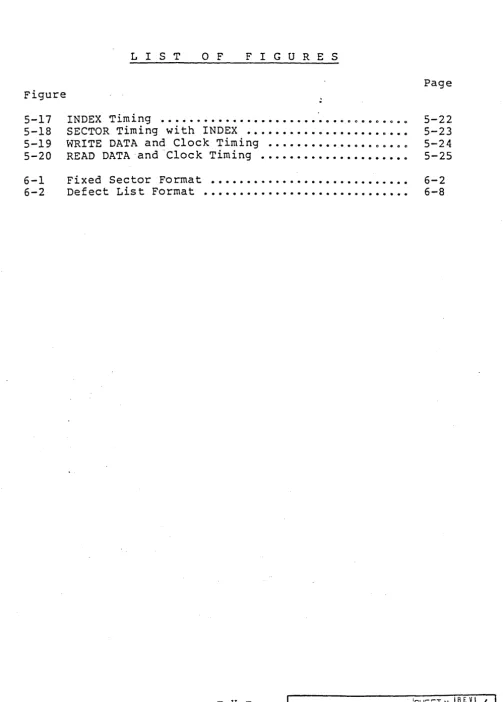
LIS T
o
F FIG U RES Figure 2-1 2-2 2-3 2-4 2-5 2-6 3-1 3-2 3-3 3-4 3-5 3-6 3-7 3-8 3-9 4-1 4-2 4-3 4-4 4-5 5-1 5-2 5-3 5-4 5-5 5-6 5-7 5-8 5-9 5-10 5-11 5-12 5-13 5-14 5-15 5-16Structure of DK512 • • • • • • • • • • • • • • • • • 0 • • • • • 0 0 0 • • 0
Spindle Motor •••••. ~ ••••.••••••..••••.•••••• o . o
Ac tua tor Arm As sembly . . . .. Air Circulation Inside Head and Disk Assembly •• Head and Cylinder Address ••..•.•.••••••••••••••• Voltage Utilization ••••.•••.•.••.••••••••••••••
DK512 PC Boards and Interface Connectors ••••••• Mounting positions .••••.••.••.•••...••••.••••••
DK512 Mountiog Dimensions: Side and Top Views •
An Example of Forced Cooling ••••.•••••.••..•.•• Cable Connector Locations •.••...••••••••••••.••
DC Power Cable A Connector J3 . • . • • . • . . . • . • . . . • .
Frame Ground Cable D Connector J4 •••••.•.••••••
.Control Cable B Connector Jl ••..•••••••••••••••
Da ta Ca.ble C Connec tor J2 ••••.••••.•••.••.••••••
+12 V DC Power Requirements ••.••••••.•••.••••••
Daisy-Chain Connection •••••••.••• ~ ••••• , •••••.•••
Star Connectionc •••••••.••• ·~ •••••.••••••••.••••• o
TTL In terf ace Ci rcu i t . . . 0
Data Interface Circuits .••.•••••.••••••••.••• 0 0
SERIAL Mode Block Diagram ••..••.••••••..•..•..• Control Cable B Signals . . . .. D'a ta Cabl e C 'S ignals . . . . HEAD SELECT Timing with WRITE GATE and
READ GATE . . . .
WRITE GATE Timing When Formatting •••••.•••••••• WRITE GATE Timing When Writing Data •••••••••••• WRITE GATE Timing with READ GATE ••.•.••.•••••••
WRITE GATE Timing with HEAD SELECT ••.••• ~ ••••••
READ DATA Timing . . . • . . . ~ . . . • . . . •
COMMAND DATA Transfer Timing with TRANSFER REQ and TRANSFER ACK . . . • . . . • . . . 0 • • • • •
Command Data Word Structure . . . .. TRANSFER REQUEST and TRANSFER ACKNOWLEDGE
Timing . . . .
DRIVE SELECTED Timing with DRIVE SELECT and
Control Signals . . . . READY Tim ing . . . . CONFIGURATION/STATUS DATA Configuration . . • . . . Typical Serial operations . . . .
- iv
-K
6600074
Page 2-2 2-6 2-7 2-9 2-10 2-11 3-1 3-2 3-3 3-4 3-6 3-6 3-7 3-7 3-8 4-1 4-2 4-3 4-4 4-5 5-2 5-3 5-4 5-7 5-8 5-8 5-8 5-9 5-9 5-10 5-11 5-14 5-15 5-16 5-16 5-21
SHEET No.1 R ;0 y \ /
Figure 5-17 5-18 5-19
5-20
6-1 6-2
L I S T
o
F FIG U RESINDEX Timing . . . • . • • . • 41 • • • 0 • c 0 c • • 0 • 0 • 0
SECTOR Timing with INDEX ••.••••.••••••.•••. 0 • • •
WRITE DATA and Clock Timing •••••••••••.••. c o . o o
READ DATA and Clock Timing •••••••••••••••••••• 0 Fixed Sector Format ••••.••.•.••••••••••.••••••• Defect List Format •••••.••••••••••.••••••.•••••
- v
-K
6600074
Page
5-22 5-23 5-24 5-25
6-2 6-8
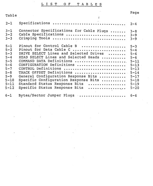
[image:10.618.69.573.54.756.2]Table
2-1 3-1 3-2 3-3
5-1 5-2 5-3 5-4 5-5 5-6 5-7 5-8
5-9
5-10 5-11 5-12
LIS T
o
F TAB L E SSpecifications
• • • • • • • • • • • • • • • • • • 0 0 G • 0 0 • • • • G • 0 e Q
Connector Specifications for Cable Plugs ••.•• 0 0
Cable Specifications ••.••••••..•••••..••.•••••• . Cr imp ing Tools ... ..
Pinout for Control Cable B
...
Pinout for Data Cable C •••.•••••.•...••••.••••• DRIVE SELECT Lines and Selected Drives 0 • • • • • • •
HEAD SELECT Lines and Selected Heads ..••.•••.•• COMMAND DATA Definitions •••• 0 • • • • • • • • • • • • • • • • • • _ _
CONFIGURATION Definitions ••••••••.••.•••••••••• CONTROL Definitions •..•••••••.•••••••••.••••••• TRACK OFFSET Definitions ••••••.•••••••••••••••• General Configuration Response Bits •••••••••••• Specific Configuration Response Bits •••••••••••
Standard Status Response Bits ••••••.•••.•.•.••
Specific Status Response Bits •..•••..•••.•.•.••
Page
2-4
3-8 3-9 3-9 5"";'3 5-4 5-6 5-6 5-11 5-13 5-13 5-14 5-17 5-18
5-19
5-20 6-1 Bytes/Sector Jumper Plugs· •••.•.••.•••• 0 0 0 . 0 • • • 6-6
vi
-'Hr-E- IRE V \ I
K
6600074
~10/
It. I Nc.l*s·
j 1m [image:11.618.72.564.97.695.2]1. INTRODUCTION
1.1 Purpose
This manual is intended to familiarize Orig!nal Equipment Manufacturers (OEMs) with the Hitachi DKS12 Winchester disk drives, and to enable OEMs to integrate the drives into their computer-based systems. The manual provides technical infor~ mation needed by system designers, engineers, purchasing
agents and quality-control personnel. A separate Service Manual describes installation, strapping, spare parts, and troubleshooting.
1.2 Manufacturer
The DKS12 series disk drives are manufactured at the Odawara
T.J--r''''''' .'u r.,..;;;" a me ... '1 'I.' be ... '- OF ... +-hQ U;+-ac hi romp,ut-t:lr v , " ' ' - A.&"''''''' . . . ..,.... D;~T;c;on • • • 'T'he ... Oda~,7~""~ " .. "-'60 .... """""
Works also produces large disk drives, magnetic tape drives, diskpacks, optical character readers, mass storage units, and data entry systems. Its first Winchester drives were deliv-ered in 1976.
1.3 Quality Control
Production of the DKS12 drives is highly automated, using robots and the latest technological advancements. The drives benefit from total vertical integration: heads, platters and electronics are all designed, manufactured and tested at the same facility; providing assurance of ~omponent compatibili-ty_ ~~ elaborate quality control system assures that each drive satisfies all specifications.
1.4 Related Documents
The following documents are also applicable. • Service Manual
• Schematic Diagrams
• Hitachi Technical Report on DKS12
1-1
2. PRODUCT DESCRIPTION
The Hitachi DKS12 series disk drives are high-capacity 5.2S-inch Winchester disk drives with an Enhanced Small
Device Interface (ESDI). The drives support" the serial
mode.
The mechanics and electronics are similar to DKSll series disk drives, which are already being marketed, but these new drives feature larger storage capacities, and higher
transfer and access speeds.
2.1 Models
The series includes three models, differing in the number of
disks mounted on the~spindle:
Model
DK512-8 DK5l2-l2 DKS12-17
Disks
3 4 6
Capacity (MBytes) (Unformatted)
86.1 120.6 172.3
The unit is housed in an aluminum casting (see Figure 2-1)0
One casting accommodates all models.
2.2 Components
The DKS12 disk drive includes the assemblies below and is
delivered with the following documents attached. Sections
3.7 and 3.8 list the connectors and cables which the customer should prepare.
2.2.1 DK512 Disk Drive Unit
Figure 2-1 shows the DKS12 disk drive unit.
The unit consists of:
eHead and Disk Assembly (HDA) eMounting Frame and Shock Mounts
.Printed Circuit (PC) boards. These are mounted in the
frame
2-1
K
SHEET NoI
R NED V \ /
2.2.2 OEM Manual, Service Manual and Schematic Diagrams
One set of these transparencies is delivered with the first
lot of drives. - When any modification is ma~en, the
corres-ponding transparency will be provided.
2.2.3 Test Report and Defect List
One set of the Test Report and the Defect List will be provided with each drive.
Voice Coil Motor
Rea:./
SpincUe. MoCOr
HDA.
Mounting Frame
Figure 2-1 Structure of DK512
2-2
2- .. 3
Op--t-ie-n-s---o Controller Board
The optional controller board enables a drive to operate with the SCSI interface.
2.4 Features
Hitachi drives are designed and manufactured for exceptional
performance and high reliability. Each drive is given a
lengthy burn-in, then tested at marginal conditions.
The principal features of the drives are summarized below:
• Large Capacity, Fast Data Transfer
This is really a fiigh performance disk drive with an exceptional maximum 171 Mbytes of capacity per drive and a fast 1.2 Mbytes/sec data transfer rate=
• Compact
It took Hitachi to put all of this capacity in a body the same size as a minifloppy disk drive.
• High-Speed Access
The DKS12 offers 23 millisecond average access time thanks to positioning to heads by a
microprocessor-controlled ~otar~ voice-coil actuator.
• Superior Reliability
In-house manufacturing of all heads, disks and custom LSIs, plus strict testing throughout guarantees the highest drive reliability.
• Industry Standard Interface
The ESDI industry standard interface provides easy integration with a wide range of systems.
2-3
j ... • NO
\Sun:-T
NoIRE
VI
3
K
6600074 \
''7/
fp,s
o2.5 Specifications
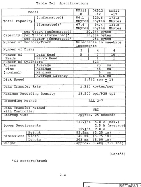
Table 2-1 lists the complete specifications for DK512 modelso
Table 2-1 Specifications
Model
[image:16.615.68.553.121.761.2](unformatted) Total Capacity
(formatted)*
per Track (unformatted) Capacity per Track (formatted)*
per Sector (formatted)* Number of Sectors/Track
~
Number of DJ.sks
Number of Data Head
Heads Servo Head
Number of CylJ.nders
Access Average
Time Maximum
(nominal) MJ.nJ.mum
Average Latency Disk Speed
Data Transfer Rate
Maximum Recording Density Recqrding Method
Data Transfer Method with Controller
Startup TJ.me
Power Requirements Height Dimensions WJ.dth -_.
Length Weight
*64 sectors/track
2-4
DKS12 DK512 DK512
-8 -12 -17
86.1 120.6 172.3 Mbytesl Mbytes Mbytes 67.4 94.4 134.8 Mbytes Mbytes Mbytes
20,944 bytes 16,384 bytes 256 bytes
Selectable J.n one-byte increments
3 4 6
5 7 10
1 1 1
823
23 ms 45 ms 6 ms 8.6 ms 3,482 rpm
+
1%-.'
1,215 kbytes/sec 18,500 bpi/925 tpi
RLL 2-7
Approx. +12V+5%
-+5V+5% 82.5mm 146 mm 203 mm Approx.
K
NRZ
25 seconds 5.0 A (max. ) 2.5 A (average) 2.8 A
(3.25 in) (5.75 J.n) (8.00 in)
3.4Kg ( 7 .5 1bs)
(Contld)
ISHEET
tnl
R HED Y 5Table--2:;.;;r----Spec::i"ficat:ion-s - (con-t tdl
Mode-l DK5l2
I
DK5l2I
DK5l2-8 -12 -17
Interface Type ESDI
Confl.guratl.ons Daisy-Chain or Radial
Acoustl.C nOl.se - Max 50 dBA; except when
start-up, stop and seek.
MTBF 20,000 POH, typical usage
Preventl.ve
Not required
Reli- Maintenance
ability MTTR 0.5 hrs
Start/Stop Up to 10,000
Operations Component
5 years or 20,000 POH Design Life
Error Rate Recover~ble
1 per 1010 bits read
(within 10 (soft)
retrials) Unrecoverable 1 per 1013 bits read
(hard) I
1 6
Seek Error Rate per 10 - seeks
Altl.tude
Operating 3,000 m (10,000 ft) max.
Nonoperating 12,000 m (40,000 ft) max.
Temperature
Operating 5°
-
45°C (41°-
113°F)Nonoperating -20° - 50°C (-4°
-
122°F)Transporting/ -40° - 60°C (-40°- 140°F)
Ambient storing
Maximum Gradient 10°C/hr. (18°F/hr.)
Relatl.ve Huml.dl.ty
Operating 8 - 80% (no condensation)
Nonoperating 8 - 90% (no condensation)
Vl.bratl.on
Operating 0.25G max.
Nonoperating 0.5G max.
Shock _
Operating 2G max. (10 msec,half sine wave)
Nonoperating 20G max. (10 msec,half sine wave)
Al.r Cleanll.ness No corrOSl.ve gas, salt, or
metallic particulates. Maxl.mum number of
86 120 172
defects per device
Maxl.mum number of
J
40 40 40Media defects per surfac
defects Detect Free Areas I Heads 0 and 1 on Cyll.nder 0
Each defect l.S l.dentifl.ed
Logging in a written test report,
and on the disk itself.
2-5
K
I'Hf:"~T j ... --. LI_I R E ·"""1 NO vI 52.6 Standards Observed
The DK5l2 drives will comply with the following standards: .
UL 478
CSA 22.2-154
FCC Part
IS,
Class A (when mounted in a standardcabi-net)
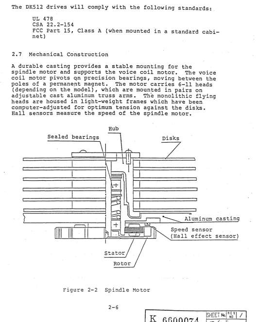
2.7 Mechanical Construction
A durable casting provides a stable mounting for the
spindle motor and supports the voice coil motor. The voice
coil motor pivots qn precision bearings, moving between the
poles of a permane~t magnet. The motor carries 6-11 heads
(depending on the model), which are moun~ed in pairs on
adjustable cast aluminum truss arms. The monolithic flying
heads are housed in light-weight frames which have been computer-adjusted for optimum tension against the disks. Hall sensors measure the speed of the spindle motor.
Sealed Disks
Aluminum casting
sensor
effect sensor)
Figure 2-2 Spindle Motor
2-6
K
6600074
SHEET17/
thl
19-7. R NEO v I, •I
I I [image:18.617.61.589.118.780.2]Actuator Arm
Disks
Coil
Figure 2-3 Actuator Arm Assembly
The disk platters are made with the aluminum substrates, which are turned with diamond tools to mirror finishes and
parallel surfaces. Proprietary processes then produce
uniform magnetic coatings. Every platter is tested ·and
inspected at each step of production.
2-7
K
6600074
I
ISHEET No.1 R ~fo vI /
2.11 Disk Basics
The spindle rotates at 3,482 rpm, creatin~ air films over the
surfaces of .the disks, which balance the p~cssure of the
flying heads· and prevent the heads from t.~juching the
surfaces. When the disks stop, as when power is turned off,
the heads come to rest in a safe area near the center of the
disk • . Close head-to-disk s~acing requires that the disks be
sealed in a clean environment.
Figure 2-4 Air Circulation Inside Head and Disk Assembly
A positioning system for the voice coil motor moves the head assembly rapidly and accurately to the addressed cylinder. Since all heads are mechanically fastened together, they are positioned to the same cylinder, that is, to the same track
on each surface. Cylinders are numbered from 0 at the
periphery to 822. at the center.
2-9
K
6·600074
SHEET No.1A NED V I I
Absolute cylinder position is established by the servo tracks, which are recorded at the factory on a dedicated surface, located at the top of the stack.
An elaborate feedback system centers the servo head in
its track,
TRACK No.
_-... A---...
( 0 1 2 821 822 \
DISK
DISK ROTATION
DATA BAND
SERVO BAND
OKS12
-17
OUTER GUARD BAND 1
OUTER GUARD BAND 2 INNER GUARD BAND
Figure 2-5 Head and Cylinder Address
An index signal and a precision clock are derived from the servo information. The index signal marks the beginning of a track or cylinder. The clock, a Phase Locked Oscillator (PLO), is a precision reference for writing data to the disk, and enables data to be formatted with shorter ~aps between
fields.
Disks are formatted by the OEM, depending on the intended application. Recommendations for a fixed sector format are provided in Chapter 6.
K
6600074
\~H;:-;:-T No.1REV I I
~ _.... tiD
2.12 Power Supply
The drive requires +12 V DC and +5 V DC input.
Figure 2-6 shows the derived voltages and representative cir-cuits operated by each voltage.
Input Derived Circuit Supplied Derived Input
1+12 vl--~---~ Spindle Motor,
Voice Coil Motor
I
+5 V ,Servo Circuit ~ -12 V
H
+12vi
Read/Write
_<~~~
.Pre-Amps in HDA
+8.3 V I---~ Servo Pre-Amps
in
HDA~
____________~:~
TTL, ECL- - Line Drivers
and Receivers, EeL Read Amps, Servo Signal Amps
Figure'2-6 Voltage Utilization
2.13 SZl18 Read/Write PC Board
This PC board controls the drive's read and write operations. Mounted on this board are:
•
•
•
•
•
•
Write driver
READY and SELECTED Lamp(LED)
Head select circuit Write fault sensor
Read signal amplifier and AGC (Automatic Gain Control)
Read signal equalizer amplifier
2-11
ISH~ET No,! Rtfo v
I
52.14 SZ123 Digital PC Board
This board controls digital operations such as interface
control, seek control, servo control and r.ead/write logic.
Mounted on this board are:
• Line drivers and receivers
• One-chip microprocesser
• Head velocity digital-to-analo~ conv~rter
• Address mark detector
• Low-voltage detector and power-on reset
• R/W gate control
• Cylinder address register
• STATUS circuit
• PLO (Phase~Locked Oscillator) for master clock • VFO (Vari~ble Frequency Oscillator) for READ DATA
• Read peak sense logic
• Write precompensation
• RLL 2-7 encoding and decoding (for writing to the
disk)
• Servo logic
• Servo signal amplifier
• position signal generator
• Sync pulse generator
2.15 SZl17 'Analog PC Board
This board controls analog operations such as motor control,
servo control and power supply. Mounted on this board are:
• Head positioning control On-track signal sensor
Track crossing pulse generator 'Absolute velocity signal generator
Velocity error signal generator • voice coil motor driver
• Voltage regulator (+2 V) • DC~DC converter (-12 V)
• DC spindle motor control
2-12
2.16 Microprocessor
A high-speed 64-pin CMOS one-chip microcomputer is
employed.-This has reduced remarkably the size of circuits. Its main
functions are:
o Motor power-on sequence
• Positioning the heads at the addressed cylinder,
using a fast seek algorithm
• Returning the heads to the zero cylinder during
power-up and recalibration (RTZ)
• Command protocol control
• Spindle motor speed checking
2-13
I{
6600074
SHEET 24-/ No.1les-
Rrio v~.
I /
/
3. PHYSICAL INTERFACE
3.1 Physical Description
The OKS12 S.2S-inch disk drive is shown in the frontispiece
and in Figure 3-1. Three cables (control, data, and power)
plug in at one end of the DKS12 PC assembly; connectors for cables to the Head and Disk Assembly (HOA) are at the other end where the Read/Write PC Board is attached, i.e., on the
Front Panel side. The Read/Write PC Board is screwed to a
heavy cover used as a heat sink; i t is connected with two
plug-in cables. The HOA is sealed in a contaminant-free
atmosphere in its casting and is never to be opened in the field.
Interface connectors
data
control po\.:er
Figure 3-1 DKSl2 PC Boards -and Interface Connectors
Figure 3-2 shows how the drive may be mounted either
hori-zontally or vertically_ Forced or natural air cooling may
be used_ When the drive is installed in a cabinet or box,
forced air cooling is required. When no fan is used, the
drive should be mounted so that the internal heat is con-ducted out completely and no outside heat affects the drive.
3-1
K
6600074
I'H-r-T No
I
n E vI
5I'" ,tr:. . un
(a) Horizontal mounting
b) Vertical mounting-l c) Vertical mounting-2
Figure 3-2 Mounting positions
3-2
K
6600074
S',r i"T 1I IRE V
I /
1
n:c. ('(0'1 NO .
3.2 Mounting Requirements
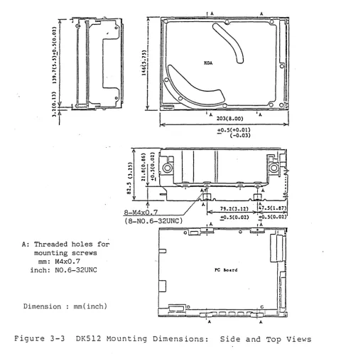
The drive has 8 threaded holes for the mounting screws.
Four screws are used, whether the drive is mounted
horizon-tally or vertically. Be careful not to insert the mounting
screws more than 5 mm (0.2 inch) into the drive.· Figure 3-3
shows the DKS12 mounting dimensions.
The guidelines in Section 3.2 should be observed by those
responsible for mounting the DKS12 in a system.
if
'o~
....
~
'""
...
,;.
:::
...
...
A: Threaded holes for mounting screws
mm: M4xO.7 inch: NO.6-32UNC
Dimension mm(inch)
r~
,..(
.... ;
."':j
·~I
~I
I
L
I~
... ... 0
r:
...C)
[image:27.620.70.551.237.735.2]...
... ~
~
N
co
8-M4xO.7
(8-NO.6-32UNC)
I A. I A.
I
203(8.00)
~
'A
+0.5(+0.01) - (-0.03)
Figure 3-3 DKS12 Mounting Dimensions: Side and Top Views
3-3
3.2.1 Shock Mounts and Handling
Special precautions must be taken so that the drive is not
jarred or bumped while it is off its shock mounts. When
r~moved from the system, i t must be placed on a urethane
foam cushion. The drive should be installed in an
acces-sible position for convenient removal and maintenancee
3.2.2 Metric Screws
Only metric screw threads and screws are used on the DK5l2. They are specified as:
M4x.7x8, where
M = Metric
4 = basic major diameter, mm. Thus, a clearance
hole would be approximately 4/25.4
=
0.157 inch.7 = di~tance between- threads, mm" Thus, this
screw has 25.4/0.7
=
36.3 threads per inch.8
=
length, mm.Metric screws must be used. There are .no U.S. Standard
screws, even inllnusual sizes, that are interchangeable"
3.2.3 Air Flow
The DK5l2 disk drives are more reliable as the ambient
tem-perature lowers. Ai~ must pass over all sides~f the HDA
and.between the boards. Select natural or forced cooling
depending on its ~ounting conditions.
3.2.3.1 Forced Cooling
When the drive is mounted in a cabinet or box, a fan must be installed on the cabinet or box to force heated air out and
take outside air in. Keep· the internal temperature as close
to the room temperature as possible. Figure 3-4 shows the
forced air flow.
Figure 3-4 An Example of Forced Cooling 3-4
3.2.3.2 Natural Cooling
Natural cooling means that the drive is mounted so that no heated air remains anywhere in the devices, and that no out-side heat affects the drive.
3-5
K
6600074
ISH'-'TI
t.t, ll_1 REV "".1.; 1mI /
/ I.'
?O / fr:. /, . j
'7'-3.4 Interface Connectors
Control cable ~, data cable C, and DC power cable A from the
controller are connected to the drive at the following con-nectors:
• Jl for Control Cable B (PI)
• J2 for Data Cable C (P2)
• J3 for DC Power Cable A (P3)
• J4 for Ground Cable D (P4)
Figure. 3-5 shows the locations of these four connectors Q
Figure 3-6 shows the DC power cable A connector J3 pinout& Figure 3-7 shows the ground cable D connector J4 :
pinout.
HDA
P2 Ground Cable D
Data Cable C Control Cable B
Figure 3-5 Cable Connector Locations
1 +12V DC
2 +12V return (CND)
3 +5V return (GND)
4: +5V DC
Figure 3-6 DC ?ower Cable A Connector J3
3-6
A
0.5(0.02)unit tnm(inch)
Figure 3-7 ~ Ground Cable D Connector J4
3.5 Control Cable B Pinout
Figure 3-8 shows the dimensions of control cable B connector
Jl.
o o
~
o
-
-
0~
tIlO
N
.
.
• 0o roo{ 0 -+1· (0.09) 2.28 +0. 15(0.006) d kness Boar Thic
1 .6 +0.1
(0.063) 5(0.OO6}
2 4
1
,-.·
I
·
I
·
, 1I
O 85(0.033)+0.09(0.0035)
Ii··
- __
1 1
O"N 34
,... ,-. ,... ~~
[
~
,.. ,..-:::-0
.
.
0 0--U'1 1.."1 I I -:::- N
II
I
.
.
~o ~ +1
II
1 .65 (0.065 ) +0.08(0.003) 2.54 (0.100 )I
I
I I 1
45.19(1.779)+0.15(0.006)
Un~t. mm(~nch)
.
Figure 3-8 Control Cable B Connector Jl
K
6600074
1-7
PIN No ..
3.6 Data Cable C Pinout
Figure 3-9 shows the data cable C connector J2.
0.85(0.033)+0.09(0.0035)
II
-
PIN No.o
o
~
.
o
\0 ..-4
.
o M 2.2 +0. Boa Thi
-
0 ..-4 \flON
.
' 0 o -+1 8(0.09) 15(0.006) rd ckness 2 ,.. I I
I
.
I
J " 1 j-
2 0 /4 ..-4_
,.. ,.. ,.. ,.. \fl ..-4
v o
. .
0 0
--
\fl \flV N
.
I I
..-40 ..-4 +1
11.65(00065) 2.54 ±O . 08 (0 • 00 3 ) (0.100) ~
I '
1.6(0.063) ~ ________________ ~=-
______________
~I
27.41(1.079>+O.15(O.006} ,:,0.15(0.006)Unit: mm(inch)
Figure 3-9 Data Cable C Connector J2
3.7 Connector Specifications for Cable Plugs
Table 3-1 lists connector specifications for cable plugs.
Table 3-1 Connector Specifications for Cable Plugs
Cable Item Mfr. Manufacturer's Part Number Oty.
B
PI Connector AMP 88373-3 1
Control C
P2 Connector
I
AMP 88373-6 1Data
A P3 Connector
Pin AMP 61314-4 4
DC Power Housing
AMP 1-480424-0 1
D 62187-1 or
P4 Plug AMP 60711-1 or 1
Ground 170038-2
3-8
K
6600074
~,I I:\:"T
I
A E VI /
3.8 Cable Specltlcatlons
Table 3-2 lists cable specifications.
Table 3-2 Cable Specificati~ns
Cable Item Length
B
Flat ribbon or twisted pair 3 m max.,
Control cumulative
C
Flat ribbon twisted pair 3 m max. , .
Data or each cable
A
20 AWG 3 m max. ,
DC Power each cable
D
Braid or equivalent, 20 AWG 3 m max.,
Ground ~ each cable
*To reduce noise, braid the cable in such cases as the cable goes out of the system cabinet.
3.9 Crimping Tools
Table 3-3 Crimping Tools
Cable Crimping tool
B Air nressure type: AHP9lll2-2
Control Manual type
-
-AHP9l085-2
C (bench type) ·
Data l-1anual type: AHP9ll28-l
A
I
l-1anual type: AMP90l23-2DC power °D
Ground
--3-9
K
6600074
SHEET ~V NoJ R NEe YII
4. ELECTRICAL INTERfACE
4.1 DC Power Requirements
Figure 4-1 gives the +12 V DC requirements. The DC brush-1 e s s mo tor re qui res a rna x i rn u m cur r en t 0 f 5 0 0 A at s tar t u p
and has short peak current requirements during seek opera~ tions.
The drive requires also +5 V DC power of 208 A.
5
4!--~---r-_...
3 --~- ---...,
...
...
... I
... I I
... L _____
+ ___ _
I I
2
1
1 I
I I
oL---~~---+_--~
I 25 I Time (sec.,)
I 1 Steady I Seek
I Startup of DC Motor I . t.
, Ooerat~on 1 Ooera ~on
, f
+12 V Power
I
(average) :DC Motor
,
3.0 A max.I
1.5 A -Other Equip. 1.0 A 1.0 A-Total 4.0 A max. 2.5 A 5.0 A max.
Figure 4-1 +12 V DC Power Requirements
Note "tha t start ing up two or more motors s imul taneously results in a large current flow. To avoid this, wait at least 20 seconds before turning on the +12 V DC power for the second motor. All the devices become ready when the last device enters the READY state.
4-1
4.2 Daisy-Chain Connection
Figure 4-2 shows the daisy-chain connection.
Control Cable B
/
Data Cable C Control /'"Signals
- ; /
1r
\/
1I
\
I \ 1 I
Data I I I
1
\ I
1
J/Terminator*2 Signals '-../I
DKSl2 DKSl2 DKSl2 DKSl2 ~
DEV#l DEV#2 DEV#N-l DEV#N DC Power r--... I
I
II
*1I \ T I
\ J
~
DC Power Cable A GroundI I
Notes
*1. N=7 for SERIAL mode.
*2. The last device (only) in the daisy-chain must have terminator on cable B. Remove the other teroinators t~at are provided ~~th
each drive. Refer to Service Manual for the locations and other necessary information.
Figure 4-2 Daisy-Chain Connection
4-2
4.3 St~r Connection
Figure 4-3 shows the star connection.
Control Cable B
J
Data Cable C/
Control f \ /
I I /
Signals \ I /
.~
/ \
Data I I
Terminator* .Signals \ '-'" I
1
~
I
f"l 'M ~ r,-:",! ,.,V~
DKS12 DKSl2 DKSl2 DKSl2 DEV#l DEV#2 ~EV#N-l DEV#N ~l
I ,
DC Power /"""..
I
-..J
I \
I
,
II I
' D C Power Cable A
Ground
I
I
Notes,
* 1 • N=7 for SERI;'.L· mode •
. *2. Each control cable is terminated at its drive. Plug-in ter-mina tors a=e provided with each drive.
Figure 4-3 Star Connection
4-3
2
4.4 Cont~ol "Signal Transmitter and Receiver Circuits
Figure 4-4 shows a single signal line in simplified form. The transmitter is a 7438 or equivalent integrated circuit
line driver which outputs TTL signals • .:The receiver is a 7414 or equivalent integrated circuit line receiver. This TTL in terface circu i t is used for all the DK512 signals except WRITE CLOCK, READ/REFERENCE CLOCK, NRZ WRITE DATA and N"RZ READ DATA.
+5 V
R2
~~~e---~) >--4--~
__~
(C Cable)
leTT:
IS
R :Rl
R2
7438
74LS14/74l4/74LS240
220n +5\ 330n ~S\
Figure 4-4 TTL Interface Circuit
The TTL interface signal transmitter and reciever circuits have the following characteristics. Note that values are those at "25°C (77°F).
• Input signal:
• High false "0": +2.5 V - +5.0 V • Low true "1" 0 V - +0.5 V
• Rise/Fall time: 30 ns max. • Output signal:
• High false "0": • Low t rue "l" • Rise/Fall time:
Open collector output 0.4 V max.
30 ns max.
4-4
K
6600074
is'H"C 11_,-~T NIH E V
I
54.5 Data Signal Transmitter and Receiver Circuits
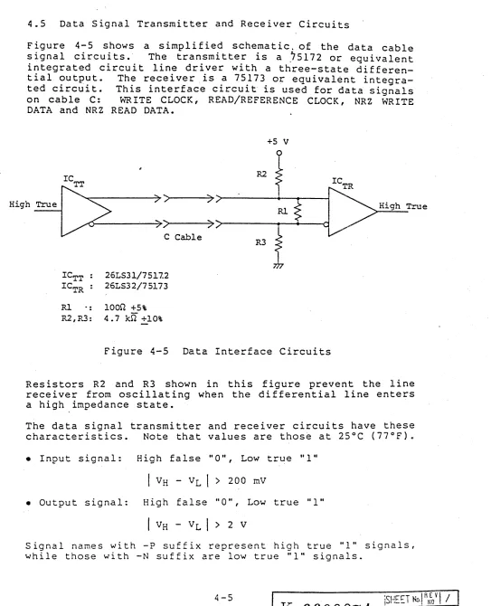
Figure 4-5 shows a simplified schematic. of the data cable s i g n a I c i r cui t s • . Th e t ran s mit t e r is a
.7
51 7 2 0 r e qui val en t integrated circuit line driver with a three-state differen-tial output. The receiver is a 75173 or equivalent integra-ted circuit. This interface circuit is used for data signals on cable C: WRITE CLOCK, READ/REFERENCE CLOCK, NRZ WRITE DATA and NRZ READ DATA.High True
+5 V
R21
ICTT
t
C2
~:»~~)"">---"">--
==
Rl
R2,R3:
- )
C Cable
26LS31/7517.2 26LS32/75173
loOn +5%
4.7 kn +10%
R3
Figure 4-5 Data Interface Circuits
High True
Resistors R2 and R3 shown in this figure prevent the line receiver from oscillating when the differential line enters a high impedance state.
The data signal transmitter and receiver circuits have these characteristics. Note that values are those at 25°C (77°F)o
•
Input signal: High false "0", Low true "l"I
VH-
VL>
200 mV•
Output signal: High false 110", Low true "I"I
VH - VL>
2 VSignal names with -P suffix represent high true "III signals,
while those with -N suffix are low true 11111 signals.
4-5
[image:38.612.63.606.96.766.2]5. INTERFACE SIGNALS -- SERIAL MODE
This chapter describes the interface s~gnals and timing· requirements. for the ESDI interface SERIAL mode implemen-ta t ion. Signal timing spec if icat ions are; those measured at the connector pins in the drive.
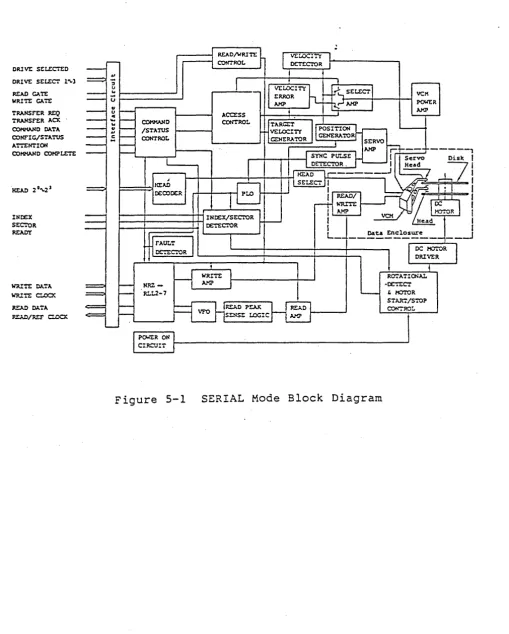
Figure 5-1 shows the DKSl2 block diagram for SERIAL mode implementation. First, the drive is selected, then the cylinder, finally the head. The desired sector is obtained by reading the sector addresses passing under the head. Each track has sync patterns and intersector gaps. WRITE GATE is asserted and negated in designated places in these fields, producing write splices. The servo information keeps the heads on cylinder, and develops the clock for encoding and decodlng the data.
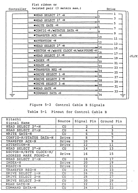
Table 5-1 lists the pinout for control cable B and Table 5-2 the pinout for data cable C.
Section 5.1 covers the control signals and Section 5 .. 2 the data signals.
5-1
T r
.t\.
6600074
DRIVE SELECTED
DRIVE SELEC'r 1"\.]
READ CAn: WRln: CAn:
TAANSrER JU:Q
TRAHSrER ACX
COM/i.'.ND DATA COHrIC/STATUS ATn:NTIOH COMMAND COKPLtn:
HEAO 2°"\.2J
INt:£X
SEC'l'OR
READY
NRZ-JU.L2-7 " HOTOR
ST~/STOP
CONTROL
'I
~~,~ ~I---~---~
Figure 5-1 SERIAL Mode Block Diagram
5-2
K
6600074
iSHEET No.1 Rrfo vI /
[image:40.617.50.560.102.736.2]Flat ribbon or
Controller twisted pair (3 meters max._) Drive
-
--HEAD SELECT 23 -N
2
-HEAD SELECf 22 -N
4
-WRI TE GATE -N
6
--CONFIG -N I_STATUS DATA -N
8
-TRANSFER ACK -N
10
I
eATTENTION -Nh2
-HEAD SELECT 2 0 -N
14
-SECTOR -N / .BYTE CLOCK -N / -AM FOUND -N
16
-HEAD SELECT 2 1 -N
18
-INDEX -N 20
-READY -N 22
-TRANSFER REQ -N 24
-DRIVE SELECT 1 -N
26
-DRIVE SELECT 2-N
28
- DRIVE SELECT 3-N 30 -READ GATE -N
32
-COMMA.~D DATA -N
34
.. _- - -
-Figure 5-2 Control Cable B Signals Table 5-1 Pinout for Control Cable B
Hitachi
I
Source
I
Signal . ! dSianal Name Pln
I
GrounHEAD SELECT 2j -N
I CU
I
2 1HEAD SELECT 2~-N I CU I 4 I 3
w'"RITE GATE-N CU I 6- 5
CONFIG-N/STATUS DATA-N Drive
I
8 7TRANSFER ACK-N Drive
I
10 9ATTENTION-N I Drive
I
12 11HEAD SELECT 2u-N CU
I
14I
13SECTOR-N/BYTE CLOCK-N/
I
DriveI
16 15ADDRESS MARK FOUND-N
HEAD SELECT 2.1.-N CU
I
18 17INDEX-N I Drive
J
20 19READY-N Drive I 22 I 21
TRANSFER REQ-N
I
CUI
24I
23DRIVE SELECT 1-N I CU I 26 I 25
DRIVE SELECT 2-N I CU I 28 I 27
DRIVE SELECT 3-N
I
CUI
30I
29READ GATE-N I CU I 32 I 31
COMMAND DATA-N I CU
,
34 I 33Notes
CU: Control Unit
-N: Low true (logical "1") signal
1
-3 --.
5
-7 --.
9
-11_13~
15 _ 1 7 1 9 2 1 23 2 5
2 7
2 9 3 1 3 3
---=-
-Pin , Jl/P1 5-3
K
I
'SHE [T No
I
f\fo v
I
3
[image:41.620.88.554.57.708.2]Flat ribbon or
Controller- twisted pair (3 meter-s--rnax~)-- Dr-i-ve
-DRIVE SELEcrED-N 1
-SECTOR -N I-BYTE CLOCK -N leAM FOUND-N 2
eCO~.MAND COMPL....~-N 3
eADDRESS MARK ENABLE -N
4
.;
eWRITE CLOCK -p
7
.WRITE CLOCK -N
8
eREAD/REFERENCE CLOCK-P 10 eREAD/REFERENCE CLOCK -N
11
.NRZ WRITE DATA -P 13 eNRZ WRITE DATA -N 14
eNRZ REl>~ DATA -p
17 .NRZ READ DATA -N
18
.INDEX -N 20
-
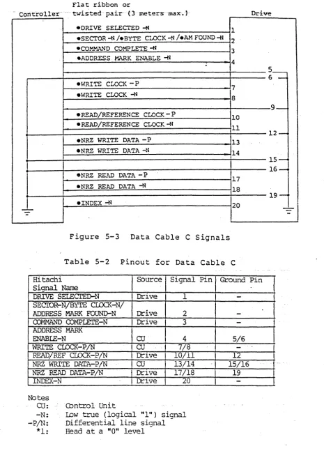
--Figure 5-3 Data Cable C Signals
Table 5-2 Pinout for Data Cable C
Hitachi 5:>urce Signal
Signal Name
DRIVE SEIECrED-N Drive 1
SECIDH-N/BYTE CIDCK-N/
ADDRESS MARK FOUND-N Drive 2
COMMAND COMPLETE-N Drive 3
ADDRESS MARK
ENABLE-N CO 4
WRITE CIDCK-PIN CO 7/8
READ/REF CIDCK-P
IN
Dr love 10/11NRZ WRITE DATA-PIN CO 13/14
NRZ READ DATA-P/N Drive 17/18
INDEX-N Dr love 20
Cbntrol Unit tbtes
CO:
-N: -PIN:
IDw true (logical "1") signal Differential line signal *1: Head at a "0" level
5-4
Pin Ground Pin
-5/6 -12 15/16 19-I{
6600074
5 _
6
9
1 2
1 5 1 6
-19
1
-
-I<:;L!--r N· !~r::::.t. [.
!
R E Y NOI
00
[image:42.617.93.559.61.722.2].;."-5.1 Control 'Signal Descriptions
This section describes the control signals transferred
be-tween the drive and the controller. One group's source is
at the controller and used to control the;drive's operation,
i.e., input signals. The other's source is at the drive and
reports its status to the controller, i.e., output signals. Control cable B transmits all the control input signals and all the control output signals except DRIVE SELECTED and
COMMAND COMPLETE which are placed on data cable C. INDEX
and SECTOR signals are found on both cables.
5.1.1 Control Input Signals
'The control input sign~ls are of two types: those to be multiplexed in a multiple drive system and those intended to do the multiplexing. The control input signals to be multiplexed are WRITE ,GATE, READ GATE, HEAD SELECT 20, HEAD SELECT 2 1 , HEAD SELECT 22, HEAD SELECT 2 3 ,
TRANSFER REQ and COMMAND DATA. The signals to do the multi~lexing are DRIVE SELECT 1, DRIVE ~ELECT 2, and DRIVE SELECT 3.
ADDRESS MARK ENABLE is a control input in the radial cable. I t is not multiplexed.
NOTE: Any lines not used should be terminated.
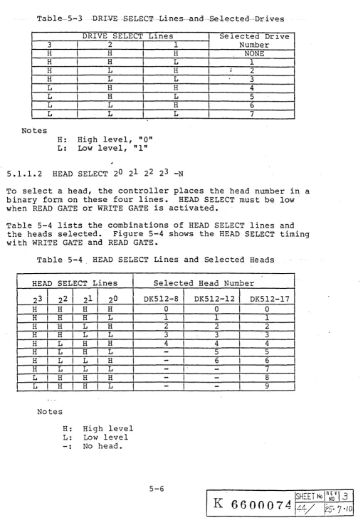
5.1.1.1 DRIVE SELECT 1, 2, 3 -N
To select a .. dri ve, the controller places the address on
these three lines in a binary form. DRIVE SELECT I" is the
least significant line and DRIVE SELECT 3 is the most
signi-ficant line. Seven drives can be selected at maximum.
Table 5-3 lists the combinations of DRIVE SELECT 1, 2 and 3
lines and the drives selected. Figure 5-13 shows the DRIVE
SELECT timing with ~ther control signals.
DRIVE SELECT must be low when SEEK, WRITE GATE, READ. GATE or STATUS CHECK command is issued.
5-5
Tabl-e---5-.,3DRI-VE -SELECT-Lines---and--Se-lected---Dr ives 3 H H H H L L L L Notes
DRIVE SELECT L1nes 2 H H L L H H L L
H: High level, "0" L: Low level, "1"
1 H L H L H L H L
5.1.1.2 HEAD SELECT 2 0 21 22 2 3 -N
Selected Dr1ve Number
NONE 1
; 2
3 4 S 6 7
To select a head, the controller places the head number in a
binary form on these four lines. HEAD SELECT must be low -when READ GATE or WRITE GATE is activated.
Table 5-4 lists the combinations of HEAD SELECT lines and the heads selected. Figure 5-4 shows the HEAD SELECT timing with WRITE GATE and READ GATE.
Table 5-4 HEAD SELECT Lines and Selected Heads
HEAD SELECT Lines 23 22 21 20
H H H H
H H H L
H 'H L H
H H L L
H L H H
H L H L
H L L
I
HH L L L
L H H H
L H H L
Notes
H: High level L: Low level -- No head.
Selected Head Number
DKS12-8 DK5l2-l2 DK5l2-l7
0 0 0
1 1 I 1
2 2 2
3 3 "3
4 4 4
-
S 5-
6 6-
-
7-
-
8-
-
9 [image:44.613.58.568.52.790.2] [image:44.613.61.494.89.307.2]HEW SELECT-N
Inv~1
Valid XI(2°, 21, 22, 2) - - - ' Inval id
I
1 ' - - 1 __---'Ir--
I-'-;"I~I- T3
I I '----_________
1,---P.E:1-J) GATE - N
RI
WRITE GATE
R$
I'
II
T 2
---i---
--I -, - T" Rl:220Q R2:330a ++
5% 5%R3:3 .9KLl
+"
5%Diode :A35DHD
or Equivalent Figure 5-4 HEAD SELECT~iming with WRITE GATE
and READ GATE
Figure 5-5A
WRITE GATE TERMINATION
5.1.1.3 WRITE GATE-N
This signal, when low, causes the serialized data on the data line to be written on the disk.
If the drive responds to the controller with WRITE FAULT while WRITE GATE remains active, the entire sector being written may be invalid. The data will be. lost, and must be rewritten after the fault has been cleared.
When WRITE GATE goes inactive upon detection of WRITE. FAULT, t-=v to rewri te the sane data if ?.E;.D"::::, S=:EK CO!-~PLET=:, H?.ITE
FAULT or H~AD S~LECT is norwal.
The following. timing restrictions apply to WRITE GATE (see Figures 5-5 through 5-8):
• When writing after reading, WRITE GATE must not b~ acti-vated for at least 300 ns after READ GATE is inactivated. • During succesive writes, as when formatting, WRITE GATE
must be inactivated for at least one microsecond between activations.
• After WRITE GATE is inactivated, READ GATE must not be activated for at least 20 microseconds.
• After the desired data is written to the diSK, one byte of
du~rny data· must be written.
5-7
K
6600074
ISHEET45/
No.1 R N~ v I 5 [image:45.617.67.567.73.763.2]INDEX-N or
SECTOR-N WRITE GATE-N
FORMAT
INOEX-N
or
SECTOR-N
rORJ1AT
READ CATE-N
WRITE. GATE-N
U
I
II
0*1
PLO BYTE ADDRESS ADR WRITE ISG SYNC CHECK ADR
SYNC
PATTERN FIELD BYTES P1\D ~PLICE
~
0.6 us max.*, .
WRI':'E GATE may remain active for the portion indica tedby "
Figure 5-5 WRITE GATE Timing When Formatting
Lf
PLO . BYTE ADDRESS iADR AOR WRITE PLO BYTE DATA I SG SYNC· SYNC FIELD /:HECK SYNC DATA
PAD SPLICE SY:~C FIELD P.t..D !SC PATTERN ~YTE:S Ph.TERN
!Ii!
I~O Bytes min 1 bit min.11----~I~
_______________________________
~Ir---I
~I
L - - - -_ _ _--JI
\,JS min.
Figure 5-6 WRITE GATE Timing When Writing Data
HRlTE GATE-N
READ GATE-N
20 l.JS min.
figur-e 5-7 \~ITE GATE Timing with READ GATE
[image:46.617.61.546.91.782.2]WRITE GATE-N
1
I
HEAD SELECT-N
I
"F
(2° '\. 23)
f
I
1 l.JS min.I'
I lJS min.i
Figure 5-8 WRITE GATE Timing with HEAD SELECT
5.1.1.4 READ GATE-N
~
. When low,'READ GATE enables the read circuitry to decode the
RLL 2-7 data written on the disk. The data is converted to
the NRZ format and, synchronized with READ CLOCK signals, transferred bit by bit to the READ DATA line, which carries i t to the con troller •.
These timing restrictions apply to READ GATE. Figure 5-9
shows the READ GATE timing •
• The characteristics of the drive circuit require a delay
when changing heads. Data can be read without error 20
microseconds after the selection of the new head. Ignore
the data for about 4 bytes after READ. GATE is activatede See Figure 5-4 •
• READ GATE must not be activated for 20 microseconds after
WRITE GATE is inactivated. See Figure 5-7.
INDEX-N
or
SECTOR-14
fORMAT
READ GATE-N
I SG PLO SYNC
I
"',
I
BYTE ~DR
AD~IU:SS ~!i~CK
SYNC
PATTERN fIELD F\"~ES
I
lEO Bytes min 1 bitPLO BYTE DATA DATA ADR WRITE
SYNC
PhD SPLICE SY:~C fIELD PAD
Ph7TERl~
min .11
I I
I-
1!SG
I
READ DATA
I
~#//7//w#/7///~
I
W///ff~//~
I I
4 bytesI
I
4 bytesI I
*1. READ GATE must be activated at least 10 bytes
prior to SYNC PATTERN after WRITE SPLICE.
Figure 5-9 READ DATA Timing
[image:47.617.57.550.109.744.2]5.1.1 .5' COMMAND DATA-N
To issue a command, the controller must send out 16-bit serial data, MSB first, and a parity bit onto this line. Transfer of this serial data is controlled by the handshake protocol with TRANSFER REO and TRANSFER ACK. Upon receiving this serial data, the drive executes a function as specified by the bi t conf igura tion. Figure 5-10 shows the COMMAND DATA transfer timing with TRANSFER REO and TRANSFER ACKo [igure 5-11 shows the COMMAND DATA bit configuration. Table 5-5 lists the COMMAND FUNCTION definitions. The following paragraphs describe each of the command functions.
While COMMAND COMPLETE is high, the controller must not send out data.
COMMAND DATA must be high when not in use.
TRANSFER REQ-N - - - "
50 ns min.
I
!
I
1°, ns min.: {
CO~.MAND D A T A - N _ Valid
~
'0 ns min. 50 ns min. I
,0
ns nu.n. •10 InS
max. 10 ms max. 110 maxo InS ~O ~O ns InS max 'no*l 0 r - - I - - - ; f
TRANSFER ACK-N
~---~
*1. Except for the last bit.
Figure 5-10 COMMAND DATA Transfer Timing with TRANSFER REO and TRANSFER ACK
5-10
[image:48.624.85.583.139.786.2]