Path Optimization for Line Scanning on Flat Panel
Displays Using a Self Organizing Map
H. A. Abeysundara
1,*, Hiroshi Hamori
1, Takeshi Matsui
2, Masatoshi Sakawa
21Research and Development Division, OHT Inc, Fukuyama, Japan
2Department of Electrical Systems and Mathematical Engineering, Faculty of Engineering, Hiroshima University, Japan
*Corresponding Author: [email protected]
Copyright © 2014 Horizon Research Publishing All rights reserved.
Abstract
This paper presents a methodology for optimization of line scan path on fixed panel displays (FPD) using a modified self organizing map (SOM). The existing scanning method of defective thin film transistor (TFT) lines on FPDs by a non-contact moving sensor is top down and unidirectional which is time consuming. First, the problem is approximated to a well known asymmetric traveling salesman problem (TSP) with precedence constraints. Then the SOM based TSP solver is proposed together with modifications for neurons before mapping them onto input space. Finally, simulation results are presented and shown the feasibility and superiority of proposed method over the existing method.Keywords
Traveling Salesman Problem, Self Organizing Map, FPD Defect Detection, TFT Line Scan1. Introduction
In modern automated factory environments, especially in semi-conductor manufacturing industry, optimization of every possible task is always paramount. With the stiff competition among manufacturers for high throughput product lines and low priced manufacturing, the flat panel display (FPD) manufactures have recently been emphasizing more research on optimization of every task. The demand for larger sizes of mother glass of FPDs (eg: Generation 10,11,12) as well as the demand for high density thin film transistor (TFT) pitch patterning of FPDs with emergence of ultra high definition 4K and 8K TVs is also another factor that any manufacturer would compel to enforce adopting speedy operations to improve competitiveness. In process flow of FPD manufacturing, inspection of TFT lines for electrical defects is one of important early processes, which will enable those defects to be repaired and restored.
Among several inspection methods of defect lines on FPDs, currently used by manufacturers, such as automatic optical inspection method, pin probe method and non-contact inspection method, the capacitor based non-contact inspection method proposed by Hamori et al. [1-6] is the most promising technique to date. Although the
defective lines (with open/short circuits) can be detected in a promising manner by this sensor, the currently used motion path of the line scan sensor for locating exact positions of defects is a simple top-down unidirectional way, which is time consuming.
In this paper, we approximate finding the shortest path of line scan to a precedence constraint asymmetric travelling salesman problem and propose a modified self organizing map or a Kohonen network based solution. A TSP is a famous NP-hard problem and one of the most difficult combinatorial optimization problems typically solved using various heuristics. It has various practical applications in industrial productions, logistics transportations, semi-conductor industry etc. However the solving leads to difficulty when it incorporates various types of precedence constraints.
In the literature of various TSP solvers, Blazinskas and Misevicius [7] have proposed a method using k-opts (2-opt, 3-opt and 4-opt) with k-swap-kick perturbations for non-constraint symmetrical TSP. They have applied k-opts with repeated breaking of two edges and reconnecting them in order and hence it looks to be heavily time consuming. Moon et al. [8] proposed a genetic algorithm based approach for a precedence constraint TSP (PCTSP) based on topological sort concept and showed good performance for larger sizes of cities. An automated printed circuit board assembly application was extensively studied for same PCTSP by Duman and Or [9]. Zong et al. [10] too studied the precedence constraint multiple TSPs by using a dynamic Tabu artificial bee colony algorithm.
Further, when looking at SOM based approaches, in early times Budinich [11] proposed an SOM for PCTSP and proved that it was better than simulated annealing for larger number of cities. Then Schabauer [12] proposed a method for large TSPs by parallelization of SOMs on clusters. Bai et al. [13] too proposed a fast and robust SOM based method for non-constraint TSP. An SOM combined to an evolutionary algorithm with Lin-Kerninghan algorithm was proposed for symmetrical TSP by Brocki [14].
2. Line Scanning on FPDs
In the capacitor based non-contact FPD inspection method proposed by Hamori et al. [1-4], all the TFT lines of mother glass panels are scanned across (Figure 1). During scanning, a voltage waveform is captured through the receiving electrode and those waveforms show defective lines with electrical defects (open and short circuits) as peaks and troughs on them and detection of them in effect produces the basis for detection of defects.
[image:2.595.58.299.287.400.2]Initially a pre-determined threshold level was used to detect such defective lines on waveforms [1-4]. In our previous work [5], we proposed a more feasible method to detect them using a feed-forward neural network instead of pre-determined threshold, and further improved by replacing the feed-forward neural network by an evolutionary optimized recurrent neural network [6].
Figure 1. Non-Contact FPD Inspection System
2.1. Existing Line Scan Method
However when defective lines (open/short) are observed in the above process, each of those lines have to be scanned by a line scan sensor in order to locate the exact coordinates of defect points to be used in the repair stage. The currently used motion path of the line scan sensor is a simple top-down unidirectional method which is time consuming particularly on larger glass panels such as 3m X 3m panels (Figure 2).
Figure 2. Existing Top Down Unidirectional Line Scan Path on A 3x3
Panel Layout
2.2. Approximation to a Constraint Based TSP Solver
The existing top-down unidirectional line scan method (Figure 2) is heavily time consuming for larger sized glass panels as well as for panels with higher number of defective
lines. This problem can be described as finding the shortest path of visiting each line once and only once. Further, if a line is considered as a pair of points (two tips of the line) the path of the sensor would become a path connecting a set of pairs of points. However, once an either point on a line (tip) is reached the next point must necessarily be the other point (other tip) of the line. Hence the problem of finding the shortest path within a set of points is restricted by precedence of those pairs of points. In other words, this problem can be approximated to an asymmetric TSP with a precedence constraint.
3. Scan Path Optimization by SOM
[image:2.595.314.553.385.513.2]Since this problem can be approximated to a TSP with precedence constraints, we employed a modified self organizing map and a node assignment technique to correctly position self learned nodes to input points. Kohonen [15] introduced a new type of neural network also known as a Kohonen network or a self organizing map that uses competitive and unsupervised learning (Figure 3). A Kohonen network maps data in complicated high dimensional spaces onto a low dimensional space, mostly to two-dimension, which will be easy to understand [16].
Figure 3. A Typical Self Organizing Map
Here, though a single line is considered as a pair of points, that pair of points is again considered as a single point (the middle point) in input space to the SOM. In other words a visit of the sensor to a defective line is considered as a visit to the middle of the line, and therefore the number of points in input space is equal to the number of lines.
[image:2.595.59.298.557.692.2] [image:2.595.313.551.620.762.2]Initially, a random map of neurons (nodes) is created with the same number of inputs and, without loss generality, the random neurons are placed on a circular chain in the same distance between them (Figure 4). When mapping input points to nodes, the distance from a point to a node is taken as the synaptic weight of the node (neuron). There are two approaches of mapping input points to nodes, namely Winner Takes All (WTA) and Winner Takes Most (WTM), and here WTM approach is adopted since it gives a chance not only to the best matched node but also to neighboring nodes to be adjusted. This is more appropriate particularly in cases with larger sizes of input spaces.
[image:3.595.67.515.384.765.2]In the learning process of the SOM, the synaptic weight of the best matching node (BMN) for an input will be adjusted as in the following equation and as shown in Figure 5.
Figure 5. Updating Synaptic Weights of a Node
i i i
W
W
W
→
−
λ
(1) where Wi is the synaptic weight of ith node and λ(0<λ<1) is the learning rate.
Synaptic weights of the neighboring nodes of ith node will also be adjusted as:
ij ij
ij
W
W
W
→
−
αλ
(2) where Wij is the synaptic weight of jth neighboring nodeof the ith node and α(0<α<1) is a neighborhood function.
The learning rate is decayed linearly during each iteration such as:
N r) 1 ( 0
− =λ
λ (3) where
λ
0is the initial learning rate, r is the current iteration number and N is the total number iterations.The neighborhood function (update length) is also
decayed linearly in the learning process as:
r
r r r 1
0
.
5
γ
γ
γ
+=
−
(4)Where r is the iteration number and
γ
ris the update length in the rth iteration.3.1. SOM Learning Algorithm
The learning of the SOM is performed, adhering to above mentioned protocols of change of synaptic weights, for a pre-determined n number of iterations as follows:
1. Create a set of nodes (the number of nodes is equal to the number of input points) and place them randomly on a circular chain with the same distance between them.
2. Take one input point randomly and find the BMN according to their synaptic weights (i.e. the nearest node).
3. Update synaptic weight of BMN as in Equation (1). 4. Find the neighboring nodes to the BMN and update
their weights according to Equation (2). 5. Repeat (2) to (4) for all remaining nodes.
6. Adjust the learning rate according to the Equation (3) .
7. Adjust the neighborhood function according to Equation (4).
8. Repeat step 2 to step 7 for N number of iterations.
3.2. Node Assignment Algorithm
After performing the learning algorithm for the SOM as mentioned in the above section, nodes are not yet perfectly mapped onto input point as shown in Figure 6. This leads to confusion when multiple nodes are closer to a single point and some nodes are isolated. Therefore we follow three steps when assigning nodes to points as:
1. Assign the nearest node for each point.
When assigning nodes to points in this way, multiple nodes can be assigned to a single point and there may be some isolated points without any node assignment (Figure 7).
2. In multiple assignments, delete all nodes other than the nearest node.
3. Create a new node per each node deleted in step 2 and assigned them to points where there are no assignments.
Figure 7. Assignment of Nodes to Points
3.3. Restoring Lines on to Points
[image:4.595.317.547.154.713.2]The points, assigned by nodes, are replaced by their original pairs of points (the two tips of the defect lines). However the path distance may have huge differences on the way on which direction the line of one point connects to the line of next one. In order to overcome this problem and also to avoid any possible loop within the path, we employ a greedy 2-opt algorithm for each node when restoring lines. 3-opt or 4-opt may be better but adopted 2-opt due to the time factor. Blazinskas and Misevicius [7] have also studied 2-opt, 3-opt, 4-opt and their combination in TSP. Figure 8 shows the final line restored path created by this SOM method for the input lines in Figure 4.
Figure 8. The Final Scan Path Created by the SOM
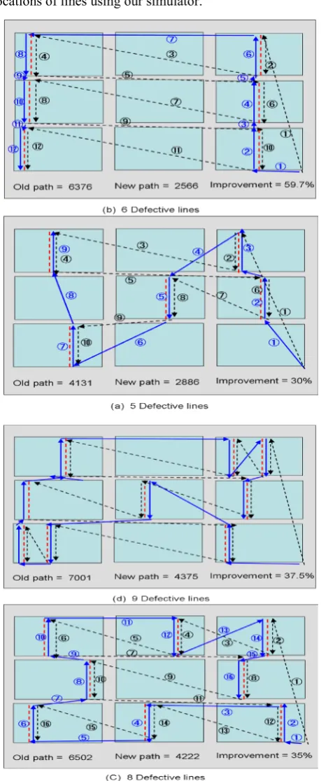
4. Experimental Results
We simulated numerous patterns of defective lines on different layouts of panels using our software. And we observed that this method improved the distance of line scan sensor by around 40%. The rate of improvement rang
1ed from 20% to 60% and the algorithm time was also greatly impressive as it was below 10 ms even for 100 lines.
Figures 9(a) to 9(d) are some selected simulated results for a 3x3 panel layout. The path distances showed in figures are the distances by GUI coordinates. The path depicted in blue color is the new SOM based path and the path in black dotted lines is the existing top down unidirectional method
in each figure. The numbers indicated the sequence on the path.
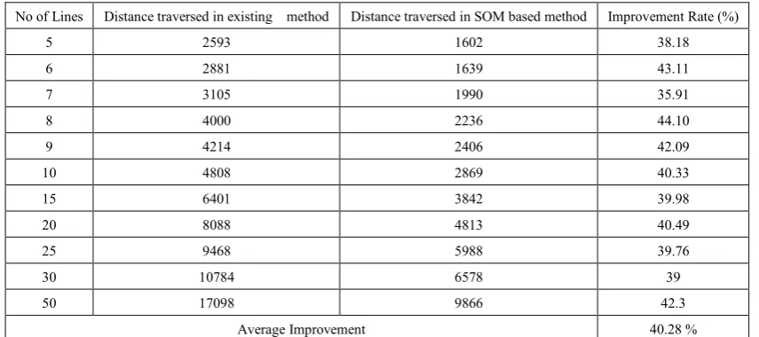
Table 1 shows a comparison of performance between our SOM based method and the existing unidirectional method for some selected number of lines. Further these figures are average distances traversed calculated of 10 random locations of lines using our simulator.
[image:4.595.57.301.407.528.2]Table 1. Comparison of Path Distance between Existing Method and Proposed Method
No of Lines Distance traversed in existing method Distance traversed in SOM based method Improvement Rate (%)
5 2593 1602 38.18
6 2881 1639 43.11
7 3105 1990 35.91
8 4000 2236 44.10
9 4214 2406 42.09
10 4808 2869 40.33
15 6401 3842 39.98
20 8088 4813 40.49
25 9468 5988 39.76
30 10784 6578 39
50 17098 9866 42.3
Average Improvement 40.28 %
5. Conclusions
In this paper, we proposed a shortest path optimization method for TFT line scanning on flat panel displays using a self organizing map. The problem was approximated to a traveling salesman problem with precedence constraints by representing defect lines with their middle points. The simulation results shown in Figures 9(a) to 9(d) for various patterns of locations of lines and various numbers of lines and the comparison between this method and the existing method shown in Table 1 confirmed the following achievements:
Path distance drop by around 40% comparatively, Algorithm time is below 10 ms even for 100 lines
which is very much acceptable.
Therefore it can be concluded that proposed method for the line scan path for FPDs based on self organizing map by adopting a constraint based asymmetric traveling salesman problem is applicable and superior than the existing top down unidirectional method.
Acknowledgements
The authors are grateful to express their gratitude to OHT Incorporation for their generous support and providing their actual data and all the other resources and facilities for this research.
REFERENCES
[1] H. Hamori, M. Sakawa, M. Katagiri and T. Matsui, “A fast non-contact inspection system based on a dual channel measurement system,” Journal of Japan Institute of electronic packaging, Vol. 13, No. 7, 2010, pp. 562-568 (in Japanese). [2] H. Hamori, M. Sakawa, M. Katagiri and T. Matsui, “Fast
non-contact flat panel inspection through a dual channel measurement system,” Proceedings of International Conference on Computers and Industrial Engineers, July 2010, CD-ROM.
[3] H. Hamori, M. Sakawa, M. Katagiri and T. Matsui, “A Defect position Identification System based on a dual channel measurement system,” Journal of Japan Institute of Electronics, Information and Communication Engineers, Vol. J94-C, 2011, No. 10, pp. 323-333 (in Japanese).
[4] H. Hamori, M. Sakawa, M. Katagiri and T. Matsui, “A Dual channel defect position identification method for touch panel manufacturing process,” Proceedings of International Conference on Electronics packaging, 2011, pp. 732-736. [5] H.A.Abeysundara, H. Hamori, T. Matsui and M. Sakawa,
“Defects Detection on TFT lines of Flat Panels using a Feed Forward Neural Network ,” International Journal of Artificial Intelligence Research, Vol.2, No. 4, 2013, pp. 1-12.
[6] H.A.Abeysundara, H. Hamori, T. Matsui and M. Sakawa, “Defects detection of TFT lines of flat panel displays using an evolutionary optimized recurrent neural network,” American Journal of Operations Research, Vol.4, No.3, 2014, pp. 113-123.
[7] A. Blazinskas, A. Misevicius, “Combining 2-opt, 3-Opt and 4-Opt with K-Swap-Kick-Perturbations for the Traveling Salesman Problem”, 17th International Conference on Information and Software Technologies, 27-29 April 2011, Kaunas, Lithuania.
[8] C. Moon, J. Kim, G. Choi, Y. Seo, “An efficient genetic algorithm for the traveling salesman problem with precedence constraints”, European Journal of Operational Research, 140, 2002, pp. 606–617.
[9] E. Duman and I. Or, “Precedence constrained TSP arising in printed circuit board assembly”, International Journal of Production Research ISSN 0020–7543 print/ISSN 1366–588X online # 2004 Taylor & Francis Ltd,
http://www.tandf.co.uk/journals, DOI: 10.1080/00207540310001601073, pp. 67-78.
[10] W. Zhong, H, Shan, Z. Chen, L. Xia, “Multiple Traveling Salesman Problem with Precedence Constraints based on Modified Dynamic Tabu Artificial Bee Colony Algorithm”, Journal of Information & Computational Science, Vol 11.4, 2014, pp. 1225–1232
[12] Hannes Schabauer, “Solving Very Large Traveling Salesman Problem by SOM Parallelization on Cluster Architecture”, Proceedings on 6th International Conference on Parallel and Distributed Computing, Applications and Technologies (PDCAT), 05-08 December. 2005, pp. 954-958
[13] Y. Bai, W. Zhang, Z. Jin, “A new self-organizing map strategy for solving the traveling salesman problem”, Journal of Chaos, Solitons & Fractals, Vol. 28, No. 4, May 2006, pp. 1082-1089.
[14] Lucas Brocki, “Kohonen Self-Organizing Map for the Traveling Salesperson Problem”, Recent Advances in Machatronics, 2007, pp.116-119
[15] T. Kohonen, “The Self-Organizing Maps”, Proceedings of the IEEE, Vol. 78, No 9, September 1990, pp. 1464-1480. [16] M. Hagenbuchner, A. Sperduti, A. C. Tsoi, “A