Spin-dependent transport
properties of Fe
3
O
4
/MoS
2
/Fe
3
O
4
junctions
Han-Chun Wu1, Cormac Ó Coileáin1,2,3, Mourad Abid2, Ozhet Mauit3, Askar Syrlybekov3,4,
Abbas Khalid3, Hongjun Xu3, Riley Gatensby5, Jing Jing Wang3, Huajun Liu6, Li Yang7,
Georg S. Duesberg5, Hong-Zhou Zhang3, Mohamed Abid2 & Igor V. Shvets3
Magnetite is a half-metal with a high Curie temperature of 858 K, making it a promising candidate for magnetic tunnel junctions (MTJs). Yet, initial efforts to exploit its half metallic nature in Fe3O4/ MgO/Fe3O4 MTJ structures have been far from promising. Finding suitable barrier layer materials, which keep the half metallic nature of Fe3O4 at the interface between Fe3O4 layers and barrier layer,
is one of main challenges in this field. Two-dimensional (2D) materials may be good candidates for this purpose. Molybdenum disulfide (MoS2) is a transition metal dichalcogenide (TMD) semiconductor
with distinctive electronic, optical, and catalytic properties. Here, we show based on the first
principle calculations that Fe3O4 keeps a nearly fully spin polarized electron band at the interface between MoS2 and Fe3O4. We also present the first attempt to fabricate the Fe3O4/MoS2/Fe3O4 MTJs.
A clear tunneling magnetoresistance (TMR) signal was observed below 200 K. Thus, our experimental
and theoretical studies indicate that MoS2 can be a good barrier material for Fe3O4 based MTJs. Our calculations also indicate that junctions incorporating monolayer or bilayer MoS2 are metallic.
Magnetite (Fe3O4), an archetypal oxide with potential applications in spintronics, has attracted a
tre-mendous level of attention in recent decades. It has a nearly fully spin polarized electron band at the Fermi level (half-metallic character) and a high Curie temperature of 858 K, which make it a promising candidate for room temperature spintronic devices and applications1–3. Recently, interesting spin
trans-port properties in Fe3O4 have been reported, i.e., a spin Seebeck effect4, a spin filter effect5, an electrical
field-induced phase transition6–8, large transversal magnetoresitance (MR)9,10, and charge-orbital
order-ing driven magnetic state switchorder-ing in Fe3O4/MgO/Fe3O4 junctions11. Yet, initial efforts to exploit its half
metallic nature in magnetic tunnel junction (MTJ) structures have been far from promising11–13. The
reduced MR attained in these investigations was attributed to the formation of a dead layer at the inter-face between Fe3O4 layers and MgO barrier layer, which reduces the spin polarization. Finding suitable
barrier layer materials is one of main challenges in this field.
Two-dimensional (2D) materials may be good candidates for this purpose. For example, graphene, an atomic-thick carbon sheet14–15, shows great potential for enhancing spin polarization. A recent
exper-iment showed that spin dependent transport at the interfaces of Fe3O4-graphene-Fe3O4 junctions
con-tributes − 1.6% MR to the whole device16. This effect can be further enhanced by inserting a thin oxide
layer such as TiO217. Unlike graphene, molybdenum disulfide (MoS2) is a transition metal dichalcogenide
semiconductor. Monolayer MoS2 is a direct band gap semiconductor with a band gap of 1.9 eV18, while
1Key Laboratory of Cluster Science of Ministry of Education, School of Physics, Beijing Institute of Technology,
Beijing, 100081, P.R. China. 2KSU-Aramco Center, King Saud University, Riyadh 11451, Saudi Arabia. 3School of
Physics and CRANN, Trinity College Dublin, Dublin 2, Ireland. 4National Laboratory Astana, Nazarbayev University,
Astana, Kazakhstan. 5CRANN, School of Chemistry, Trinity College Dublin, Dublin 2, Ireland. 6Institute of Plasma
Physics, Chinese Academy of Sciences, Hefei, 230031, P. R. China. 7Electronic Engineering Institute, Hefei, 230037,
P. R. China. Correspondence and requests for materials should be addressed to H.-C.W. (email: [email protected]) or H.J.L. (email: [email protected])
Received: 08 June 2015
accepted: 24 September 2015
Published: 02 November 2015
www.nature.com/scientificreports/
bulk MoS2 has an indirect band gap of 1.29 eV19. Recently, monolayer and multilayer MoS2 have been
shown to have a carrier mobilities of up to 200 cm2/Vs and 100 cm2/Vs at room temperature,
respec-tively, and a current on/off ratio of 1 × 10⁸, which makes MoS
2 a promising candidate for incorporation
into a new generation of more efficient transistors20. Moreover, monolayer MoS
2 has strong spin orbit
coupling with a large spin splitting of up to 456 meV in the valence band originating from the d orbitals of the heavy metal atoms21, due to the symmetry breaking21,22. Valley polarization in monolayer MoS
2
can be achieved with circularly polarized light23,24. Consequently, MoS
2 is also a fascinating material for
spintronics applications based on spin and valley control25,26. MoS
2 also has potential in
photolumines-cence sensors27, solar energy funnels28, integrated circuit devices29, chemical sensor30, and photodiodes31.
Recently, the magnetic and electronic properties of Fe3O4, MoS2 and ferromagnetic metal/Mos2 interfaces
have been investigated32–39 and the NiFe/MoS
2/NiFe Junction has been fabricated40.
In this paper, we show based on the first principle calculations that Fe3O4 keeps a nearly fully spin
polarized electron band at the interface between MoS2 and Fe3O4 and no dead layer is formed at the
interface. We also present the first report on the fabrication and characterization of MoS2 based MTJs
with ferromagnetic oxide electrode. The MTJ stacks in this work are Fe3O4-MoS2-Fe3O4 trilayers grown
on MgO (001) single crystal substrate. The quality of the MoS2 barrier layer was investigated by X-ray
photoemission spectroscopy (XPS), Raman spectroscopy, atomic force microscopy (AFM), and trans-mission electron microscopy (TEM). The magneto-transport properties were studied by the means of a physical property measurement system (PPMS, Quantum Design). A clear tunneling magnetoresistance (TMR) signal was observed at 200 K. Our results may be also valuable for understanding how MoS2 can
be used for other spintronic devices and applications.
Results
Electronic structure of Fe3O4/MoS2/Fe3O4 junctions. We employed the projected augmented
plane wave method (PAW)41, implemented within the Vienna Ab Initio Simulation Package (VASP)42.
The generalized gradient approximation43 is used for the exchange-correlation energy. In our
calcula-tions, we use a rotated MoS2 supercell constructed in a rectangular geometry and consider two reduced
Fe3O4 unit cells containing 28 atoms each, separated by a 3 MoS2 layers, as shown in Fig. 1e. We consider
MoS2 to be epitaxially grown on Fe3O4 as our experiment, thus the MoS2 is strained to match the lattice
of Fe3O4. All geometries are relaxed until the forces on the atoms are less than 0.02 eV/Å. Periodic
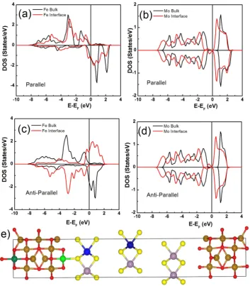
boundary conditions are employed in the plane perpendicular to the transport direction (z direction), with a monkhorst-pack 6 × 6 × 1 k-point grid for geometry optimization. In Fig. 1, we plotted the density of states (DOS) of B-site Fe (dark green ball) and Mo (dark blue ball) atoms far from the interface, and B-site Fe (light green ball) and Mo (light blue ball) atoms at the interface, for magnetization of the two Fe3O4 layers in parallel and anti-parallel configurations The MoS2 at the interface becomes metallic
behavior due to hybridization between Fe and S, which is consistent with the reports by another research group40,44. Significantly, despite the hybridization between the Fe and S, the interface Fe still keeps a
nearly fully spin polarized electron band at the Fermi level, indicating that Fe3O4 keeps its half-metallic
nature in Fe3O4/MoS2/Fe3O4 junctions and no dead layer is formed at the interface. If we do not take into
account the spin flip process when the spin polarized current tunneling through MoS2, the TMR of a
MTJ can be defined as: TMR= 1−2P PP P1 2
1 2, where P1 and P2 are the spin polarization of the two ferromag-netic electrodes. Thus, a significant high TMR is expected in Fe3O4/MoS2/Fe3O4 junctions. In the
follow-ing sections, we will describe the attempt to fabricate the Fe3O4/MoS2/Fe3O4 MTJs.
Device preparation and characterization. The Fe3O4/MoS2/Fe3O4 trilayer structures were grown
on MgO (001) single crystal substrates. The thicknesses for the bottom and top Fe3O4 layers were 60 nm
and 10 nm respectively. The Fe3O4 layers were prepared in a molecular beam epitaxy system (MBE) with
a base pressure of 5 × 10⁻¹⁰ Torr. Reflection high energy electron diffraction (RHEED) was employed to
confirm the epitaxial growth and establish the growth mode. Figure S1 shows RHEED patterns recorded in the [100] azimuth during growth, which indicates the pseudomorphic growth of the Fe3O4. Figure 2a
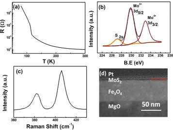
shows the resistivity as a function of the temperature (R-T) for the bottom Fe3O4 layers. The Verwey
transition is clearly present at 115 K which is close to well established bulk values, indicating the good quality of the bottom Fe3O4 layer. Details of the growth procedure and characterization are given
else-where45. MoS
2 can be obtained by the top-down exfoliation methods46, or by bottom up methods, such as
transition metal sulfurization47, molybdenum oxide sulfurization48, decomposition of thiomolybdates49,
and van der Waals epitaxy50. To fabricate few- or single-layer MoS
2 devices, most studies use
mechan-ical exfoliation or intercalation-assisted exfoliation of bulk MoS2, which results in microscale flakes of
random shapes and thicknesses. In this work, to achieve large-scale continuous MoS2 films on the
bot-tom Fe3O4 electrode, a thin Mo film was first deposited on the bottom Fe3O4 using an e-beam heated
Mo source in the MBE system. After growth, the thin Mo layer was annealed at 500 °C with an oxygen
partial pressure of 1 × 10⁻⁵ Torr for 30 minutes. Figure S1c shows the RHEED patterns of sample after
annealing in oxygen indicating the epitaxial growth of MoO on the Fe3O4 layer which also guarantees a
flat interface between MoS2 and Fe3O4. To form MoS2, the sample was removed from the MBE chamber
and sulfurized at 700 °C for 1 min to 2 min in a furnace based on the well-established vapor phase growth technique51. The chemical composition of the MoS
Mo 3d3/2, and S 2 s peaks have been consistently energy shifted in order to position the peak in the C
1 s region at a binding energy (BE) of 284.7 eV. The peak positions for the Mo 3d5/2, Mo 3d3/2, and S 2 s
are 229 eV, 232 eV, and 226 eV respectively, which are consistent with the values for bulk MoS2. From
Fig. 2b, we can also estimate that the atomic ratio of Mo: S is approximately 1:2. Raman spectroscopy was used to further evaluate the quality of the MoS2 layer. Figure 2c shows a Raman spectrum of the MoS2
film collected by a Renishaw spectrometer with a 488 nm laser at room temperature. Strong signals for both the characteristic in-plane degenerate E1
2g and out-of plane A1g modes are present at 406 cm−1 and
383 cm−1, respectively. The peak positions are close to the positions expected for bulk MoS
2. The XPS
and Raman results indicate the good quality of the MoS2 layer.
The morphology of the MoS2 was examined with AFM. The AFM image shown in Figure S2 indicates
a uniform MoS2 film on the Fe3O4. Additionally, the RMS roughness of this thin film is of 0.117 nm. The
quality of the MoS2/ Fe3O4 interface and thickness of MoS2 layer were characterized by TEM. Figure 2d
shows a typical TEM image of the MoS2/ Fe3O4 bilayer on a MgO substrate. One can see from Fig. 2d
that a 2 nm thick MoS2 film is on top of the Fe3O4 layer with a sharp interface between the MoS2 and
Fe3O4 layers. Finally, the top Fe3O4 electrode was deposited. Two different size junctions (10 × 10 μ m2
and 400 × 200 nm2) were fabricated through several steps E-beam lithography and lift-off processes as
described in the experimental section.
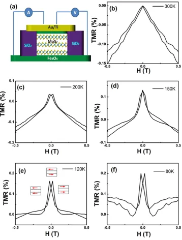
Magnetic and Transport properties. Figure 3a shows a schematic drawing of the Fe3O4/MoS2/Fe3O4
[image:3.595.160.514.45.449.2]www.nature.com/scientificreports/
into the MoS2 barrier layer from the top Fe3O4 electrode, which can then be detected by the bottom Fe3O4
electrode. It is known that the different thicknesses of the Fe3O4 layers will result in different coercivity
fields13. Figure S3 shows the M (H) loops for 60 nm and 10 nm of Fe
3O4 on MgO substrates. The
coer-civity fields for 60 nm of Fe3O4 and 10 nm of Fe3O4 at room temperature are 125 Oe and 60 Oe
respec-tively. By applying an in-plane magnetic field, the magnetization states of the device can be tuned from a parallel (P) to an antiparallel (AP) configuration, or vice versa. Figure 3b–f show MR curves of Fe3O4/
MoS2/Fe3O4 junctions measured at different temperatures. The external magnetic field was applied in the
film plane along the [100] direction. At 300 K, the resistance shows a linear response to the external field. While at low temperature, non-linear MR curves are observed. The linear MR behavior observed at room temperature is mainly due to spin-dependent transport across the anti-ferromagnetic (AF) anti-phase boundaries (APBs) in Fe3O4 layers52,53. To understand better the MR curves measured at low
tempera-ture, we show in Figure S4 the MR plots of the Fe3O4/MoS2/Fe3O4 junctions measured with a field of up
to 1 T. One can clearly see from Figure S4 that there are two main contributions to the MR: non-linear MR at low fields and linear MR at high fields due to spin-dependent transport across the AF APBs.
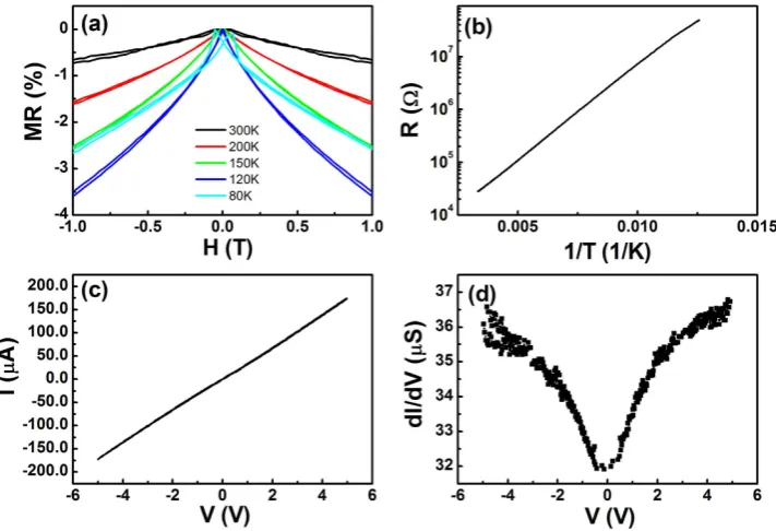
To demonstrate that the non-linear MR observed at low fields is not due to MR effects of the bottom or top Fe3O4 electrodes, we show in Fig. 4a MR curves for the bottom 60 nm thick Fe3O4 layer measured
for different temperatures. Linear non-saturated MR curves are observed for temperatures above the Verwey temperature. Moreover, the MR ratio is significantly higher than that of the Fe3O4/MoS2/Fe3O4
junctions. Below the Verwey temperature, the non-linear MR at low field is due to discrete changes in the entropy and the phonon-magnon interaction52. We also measured the MR of Fe
3O4/MoS2/Fe3O4
junctions without MoS2 barrier (Figure S5). The MR curves are very similar to that for single Fe3O4 layer.
Therefore, the non-linear MR observed in the Fe3O4/MoS2/Fe3O4 junctions at low fields cannot be
attrib-uted to the MR effect of the bottom or top Fe3O4 electrodes. Figure 4b shows the R-T plot of the Fe3O4/
MoS2/Fe3O4 junctions.The resistance of the MTJ is one order of magnitude higher than that of solely the
bottom Fe3O4 electrode and the R-T measurement shows no clear trace of the Verwey transition
indicat-ing that the resistance of the MTJ is dominated by the properties of the MoS2 layer. We fitted the R-T
curve with the relationship R T( ) ≈R0exp(K TEa)
B , which gives an activation energy (Ea) of 72 meV. The
obtained activation energy is about twice the value of that for the 60 nm Fe3O4 on MgO substrate and
even larger than the activation energy for a single AF APB52. Note, while the Verwey transition is not
[image:4.595.157.515.44.311.2]at 300 K. Non-linear IV is observed. To confirm further this non-linear behavior, we show in Fig. 3d the dI/dV as a function of the bias voltage V. The quasiparabolic dependence between dI/dV and V also suggests that the non-linear MR observed at low fields is due to the TMR effect of the Fe3O4/MoS2/Fe3O4
junctions. We can define the TMR ratio for the low field region as TMR= RAPR−RP
P , where RAP and RP are
resistances when the magnetization states of the device are in anti-parallel and parallel configurations respectively. Figure S7 shows the M (H) loop and MR curve for Fe3O4/MoS2/Fe3O4 junction measured at
200 K. To clearly see the magnetization reversal process, we have drawn schematically the magnetization states of the device in Figure S7. Therefore, the non-linear MR observed at low fields is due to the mag-netization alignments of two FM electrodes. Figure S8 summarizes the TMR ratio as a function of tem-perature. The TMR ratio increases with decreasing temperature and a TMR ratio of 0.2% is obtained at 80 K. We did not observe a sharp increase of the TMR ratio around Verwey transition which gives another indication that the non-linear MR at low fields is due to spin-dependent tunneling through the MoS2 barrier layer. Although we did not obtain a TMR ratio as significant as that predicated by our
[image:5.595.158.517.44.517.2]calculation, our first attempt does suggest that MoS2 can be used as a barrier material for Fe3O4 based
www.nature.com/scientificreports/
MTJ. One of the possible reasons for the reduced TMR ratio is that the quality of the interface between the MoS2 and the top Fe3O4 may be not as good as the interface between the MoS2 and the bottom Fe3O4
since the sample was removed from vacuum to produce the MoS2 layer. To confirm this, Figure S9 shows
the TMR ratio as a function of bias voltage measured at 200 K. One can see that TMR is asymmetric with respect to the bias voltage and has a maximum at a bias of − 1 V. This asymmetry suggests that the quality of the two interfaces is different. The bottom Fe3O4/MoS2 interface is atomically sharp, while the top
Fe3O4/MoS2 interface is rougher. It also indicates that the non-linear MR observed at low fields is due to
the TMR effect of the Fe3O4/MoS2/Fe3O4 junctions. Another possibility is that the bottom Fe3O4 may also
be partially sulfurized during the sulfurization.
In conclusion, we show based on the first principle calculations and TMR characterization of Fe3O4/
MoS2/Fe3O4 junctions that MoS2 can be a good barrier material for Fe3O4 based MTJs. Our calculations
also indicate that junctions incorporating monolayer or bilayer MoS2 are metallic. Our experimental
results may pave the way for the application of MoS2 in spintronics.
Methods
Growth of Fe3O4-MoS2-Fe3O4 trilayers. The Fe3O4-MoS2-Fe3O4 trilayers were grown on MgO
(001) single crystal substrates using a MBE system (DCA MBE M600, Finland) with a base pressure of 5 × 10⁻¹⁰ Torr. The substrates were chemically cleaned prior to their insertion into the growth chamber
and then cleaned in situ at 600 °C in UHV for 1 hour. The growth conditions for Fe3O4 can be found
else-where. The thicknesses for the bottom and top Fe3O4 layers are 60 nm and 10 nm respectively. To grow
MoS2, a thin Mo film were first deposited by e-beam from a Mo source. Subsequently, the thin Mo layer
was annealed at 500 °C with an oxygen partial pressure of 1 × 10⁻⁵ Torr for 30 mins. Then the sample was
taken out and sulfurized at 700 °C for 1 min to 2 min in a chemical vapor deposition (CVD) furnace to form MoS2 based on the vapor phase growth technique. This short sulfurization time prevents a deeper
sulfurization of the Fe3O4 layer in agreement with the XPS analysis.
Device fabrication. A multistep process was used to fabricate the Fe3O4-MoS2-Fe3O4 junctions with
two different sizes (10 × 10 μ m2 and 400 × 200 nm2). The resistance-area (RA) of the junction is around
107 Ω μ m2 at room temperature and remains constant irrespective to the junction size. A Negative tone
S1820 and MA N2403 were used for UV lithography and e-beam lithography respectively, followed by ion milling and the post exposure lift-off was carried out after SiOx deposition to insulate the top and
bottom contacts. A top contact of Ti 6 nm/Au 50 nm was deposited by evaporation with subsequent lift off.
Characterization of the Fe3O4-MoS2-Fe3O4 junctions. The magneto-transport behavior of the
[image:6.595.158.514.45.288.2]Fe3O4-MoS2-Fe3O4 junctions was examined by means of a physical property measurement system
(PPMS, Quantum Design). X-ray photoelectron spectrometer (XPS) measurements were performed in an Omicron Nanotechnology Spectroscopy system equipped with an Ar ion miller in the preparation chamber. Raman spectra was collected using a Renishaw InVia spectrometer with a 488 nm laser at room temperature.
References
1. Walz, F. The verwey transition—a topical review. J. Phys. Condens. Matter14, R285 (2002).
2. Ziese, M. Extrinsic magnetotransport phenomena in ferromagnetic oxides. Rep. Prog. Phys.65, 143 (2002).
3. Brabers, J. H. V. J., Walz, F. & Kronuller, H. The influence of a finite bandwidth on the Verwey transition in magnetite. J. Phys. Condens. Matter.12, 5437 (2002).
4. Ramos, R. et al. Observation of the spin Seebeck effect in epitaxial Fe3O4 thin films. Appl. Phys. Lett.102, 072413 (2013).
5. Liao, Z. M. et al. Spin-filter effect in magnetite nanowire. Nano Lett.6, 1087 (2006).
6. Gooth, J. et al. Gate voltage induced phase transition in magnetite nanowires. Appl. Phys. Lett.102, 073112 (2013). 7. Lee, S. et al. Electrically driven phase transition in magnetite nanostructures. Nature Mater.7, 130 (2008).
8. Wong, J. J. I., Swartz, A. G., Zheng, R. J., Han, W. & Kawakami, R. K. Electric field control of the verwey transition and induced magnetoelectric effect in magnetite. Phys. Rev. B86, 060409 (2012).
9. Fernández-Pacheco, A. et al. Giant planar hall effect in epitaxial Fe3O4 thin films and its temperature dependence. Phys. Rev. B
78, 212402 (2008).
10. Wu, H. C. et al. Transversal magneto-resistance in epitaxial Fe3O4 and Fe3O4/NiO exchange biased system. Appl. Phys. Lett.101,
052402 (2012).
11. Wu, H. C., Mryasov, O. N., Abid, M., Radican, K. & Shvets, I. V. Magnetization states of all-oxide spin valves controlled by charge-orbital ordering of coupled ferromagnets. Sci. Rep.3, 1830 (2013).
12. Li, X., Gupta, A., Xiao, G., Qian, W. & Dravid, V. Fabrication and properties of heteroepitaxial magnetite tunnel junctions. Appl. Phys. Lett.73, 3282 (1998).
13. Wu, H. C., Arora, S. K., Mryasov, O. N. & Shvets, I. V. Antiferromagnetic interlayer exchange coupling between Fe3O4 layers
across a nonmagnetic MgO dielectric layer. Appl. Phys. Lett.92, 182502 (2008).
14. Novoselov, K. S. et al. Two-dimensional gas of massless dirac fermions in graphene. Nature438, 197 (2005).
15. Zhang, Y., Tan, Y. W., Stormer, H. L. & Kim, P. Experimental observation of the quantum Hall effect and Berry’s phase in graphene. Nature438, 201 (2005).
16. Liao, Z. M. et al. Magnetoresistance of Fe3O4-graphene-Fe3O4 junctions. Appl. Phys. Lett.98, 052511 (2011).
17. Han, W. et al. Tunneling spin injection into single layer graphene. Phys. Rev. Lett.105, 167202 (2010).
18. Mak, K. F., Lee, C., Hone, J., Shan, J. & Heinz, T. F. Atomically Thin MoS2: a new direct-gap semiconductor. Phys. Rev. Lett. 105,
136805 (2010).
19. Kam, K. K. & Parkinson, B. A. Detailed photocurrent spectroscopy of the semiconducting group VIB transition metal dichalcogenides. J. Phys. Chem. 86, 463 (1982).
20. Radisavljevic, B., Radenovic, A., Brivio, J., Giacometti, V. & Kis, A. Single-layer MoS2 transistors. Nature Nanotech. 6, 147 (2011).
21. Zhu, Z. Y., Cheng, Y. C. & Schwingenschlögl, U. Giant spin-orbit-induced spin splitting in two-dimensional transition-metal dichalcogenide semiconductors. Phys. Rev. B84, 153402 (2011).
22. Ellis, J. K., Lucero, M. J. & Scuseria, G. E. The indirect to direct band gap transition in multilayered MoS2 as predicted by screened hybrid density functional theory. Appl. Phys. Lett. 99, 261908 (2011).
23. Yao, W., Xiao, D. & Niu, Q. Valley-dependent optoelectronics from inversion symmetry breaking. Phys. Rev. B77, 235406 (2008). 24. Xiao, D., Liu, G. B., Feng, W., Xu, X. & Yao, W. Coupled spin and valley physics in monolayers of MoS2 and other group-VI
dichalcogenides. Phys. Rev. Lett.108, 196802 (2012).
25. Zeng, H., Dai, J., Yao, W., Xiao, D. & Cui, X. Valley polarization in MoS2 monolayers by optical pumping. Nat. Nanotech.7, 490
(2012).
26. Mak, K. F., He, K., Shan, J. & Heinz, T. F. Control of valley polarization in monolayer MoS2 by optical helicity. Nat. Nanotech.7,
494 (2012).
27. Yin, Z. Y. et al. Single-layer MoS2 phototransistors. ACS Nano6, 74 (2012).
28. Feng, J., Qian, X., Huang, C.-W. & Li, J. Strain-engineered artificial atom as a broad-spectrum solar energy funnel. Nat. Photon. 6, 866 (2012).
29. High, A. A., Novitskaya, E. E., Butov, L. V., Hanson, M. & Gossard, A. C. Control of exciton fluxes in an excitonic integrated circuit. Science321, 229 (2008).
30. Lee, K., Gatensby, R., McEvoy, N., Hallam, T. & Duesberg, G. S. High-performance sensors based on molybdenum disulfide thin films. Adv. Mater.25, 6699 (2013).
31. Yim, C. et al. Heterojunction hybrid devices from vapor phase grown MoS2. Sci. Rep.4, 5458 (2014).
32. Mi, W. B., Shen, J. J., Jiang, E. Y. & Bai, H. L. Microstructure, magnetic and magneto-transport properties of polycrystalline Fe3O4
films. Acta Mater.55, 1919 (2007).
33. Senn, M. S., Wright, J. P. & Attfield, J. P. Charge order and three-site distortions in the verwey structure of magnetite. Nature 481, 173 (2012).
34. Mi, W. B., Guo, Z. B., Wang, Q. X., Yang, Y. & Bai, H. L. Charge ordering in reactive sputtered (100) and (111) oriented epitaxial Fe3O4 films. Scripta Mater.68, 972 (2013).
35. Feng, N. et al. Magnetism by interfacial hybridization and p-type doping of MoS2 in Fe4N/MoS2 superlattices: a first-principles
study. ACS Appl. Mater. Interf.6, 4587 (2014).
36. Yin, M. Y., Wang, X. C., Mi, W. B. & Yang, B. H. First principles prediction on the interfaces of Fe/MoS2, Co/MoS2 and Fe3O4/
MoS2. Comput. Mater. Sci.99, 326 (2015).
37. Zhang, X. J., Mi, W. B., Wang, X. C., Cheng, Y. C. & Schwingenschlögl, U. The interface between Gd and Monolayer MoS2: a
first-principles study. Sci. Rep. 4, 7368 (2014).
38. Zhang, X. J., Mi, W. B., Wang, X. C., Cheng, Y. C. & Schwingenschlögl, U. First principles prediction of the magnetic properties of Fe-X6 (X= S, C, N, O, F) doped monolayer MoS2. Sci. Rep.4, 3987 (2014).
39. Cheng, Y. C., Zhu, Z. Y., Mi, W. B., Guo, Z. B. & Schwingenschlögl, U. Prediction of two-dimensional diluted magnetic semiconductors: Doped monolayer MoS2 systems. Phys. Rev. B87, 100401(R) (2013).
40. Wang, W. et al. Spin-Valve Effect in NiFe/MoS2/NiFe Junctions. Nano Lett. (2015), doi: 10.1021/acs.nanolett.5b01553.
41. Kresse, G. & Hafner, J. Ab initio molecular dynamics for liquid metals. Phys. Rev. B47, R558 (1993).
42. Payne, M. C., Teter, M. P., Allan, D. C., Arias, T. A. & Joannopoulos, J. D. Iterative minimization techniques for ab initio total-energy calculations: molecular dynamics and conjugate gradients. Rev. Mod. Phys.64, 1045 (1992).
www.nature.com/scientificreports/
44. Dolui, K., Narayan, A., Rungger, I. & Sanvito, S. Efficient spin injection and giant magnetoresistance in Fe/MoS2/Fe junctions.
Phys. Rev. B90, 041401(R) (2014).
45. Arora, S. et al. Giant magnetic moment in epitaxial Fe3O4 thin film. Phys. Rev. B77, 134443 (2008).
46. Splendiani, A. et al. Emerging photoluminescence in monolayer MoS2. Nano Lett.10, 1271 (2010).
47. Kim, D. et al. Toward the growth of an aligned single-layer MoS2 film. Langmuir27, 11650 (2011).
48. Lee, Y. H. et al. Synthesis of large-area MoS2 atomic layers with chemical vapor deposition. Adv. Mater.24, 2320 (2012).
49. Liu, K. K. et al. Growth of large-area and highly crystalline MoS2. Nano Lett.12, 1538 (2012).
50. Ji, Q. et al. Epitaxial monolayer MoS2 on mica with novel photoluminescence. Nano Lett.13, 3870 (2013).
51. Gatensby, R. et al. Controlled synthesis of transition metal dichalcogenide thin films for electronic applications. Appl. Surf. Sci. 297, 139 (2014).
52. Wu, H. C. et al. Probing one antiferromagnetic anti-phase boundary and single magnetite domain using nanogap contacts. Nano Lett.10, 1132 (2010).
53. Eerenstein, W., Palstra, T. T. M., Saxena, S. S. & Hibma, T. Spin-polarized transport across sharp antiferromagnetic boundaries.
Phys. Rev. Lett.88, 247204 (2002).
Acknowledgements
This work was supported by Beijing Institute of Technology Research Fund Program for Young Scholars, Science Foundation of Ireland (SFI) (Contract No. 06/IN.1/I91, 10/IN.1/I3030), National Plan for Science and technology (Nos. NPST 1598–02 and NPST 1466–02) of King Abdulaziz City for Science and Technology. H.C.W., MA.A., and MO.A. thank Saudi Aramco for the financial support (project No. 6600028398). O.M. and A.S. acknowledge the financial support by the Bolashak Program funded by the Kazakhstan government. We would like to thank Prof. O.N. Mryasov for reading the manuscript and giving valuable comments.
Author Contributions
H.C.W. conceived the study. O.M., A.S. and C.C. grew the sample. A.S., H.J.X., and M.O.H.A. fabricated the sample. H.C.W. performed the magnetic and transport measurements. A.K., A.M., and H.Z.Z. carried out the TEM measurements. R.G. and G.S.D. sulfurized the sample. J.J.W. and MOU.A. performed the Raman characterization. H.L., L.Y. and I.V.S. gave scientific advice. H.C.W. wrote the manuscript. All authors discussed the results and commented on the manuscript.
Additional Information
Supplementary information accompanies this paper at http://www.nature.com/srep Competing financial interests: The authors declare no competing financial interests.
How to cite this article: Wu, H.-C. et al. Spin-dependent transport properties of Fe3O4/MoS2/Fe3O4
junctions. Sci. Rep. 5, 15984; doi: 10.1038/srep15984 (2015).