Thermal Stability of Engineered
SOI Material
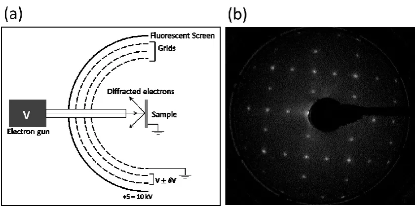
A thesis presented to the University of Dublin, Trinity College for the degree of
Doctor of Philosophy in Chemistry
2017
Barimar Prabhava Sai Narayana
Under the supervision of Prof. John Boland School of Chemistry & CRANN
I, the undersigned, declare that this work has not previously been submitted as an exercise for a degree at this, or any other University, and that unless otherwise stated is my own work. Elements of this work that have been carried out jointly with others or by collaborators have been duly acknowledged in the text.
I agree to deposit this thesis in the University’s open access institutional repository or allow the library to do so on my behalf, subject to Irish Copyright Legislation and Trinity College Library conditions of use and acknowledgement.
Barimar Prabhava Sai Narayana
I
The objective of this thesis is to provide new insights into the properties of silicon-on-oxide (SOI) and the stability and electronic structure of patterned SOI. Any freshly formed silicon surface is highly reactive and in the presence of oxygen the surface immediately forms a thin layer of oxide known as a native oxide. Surface analysis of silicon samples by scanning tunneling microscopy – a key focus of this work - requires removal of the native oxide before measurement. Removing the thin native oxide layer from silicon in an UHV environment involves annealing and processing SOI at elevated temperature in a manner that avoids damage to the device layer. The potential for modifying the chemical composition on the surface, the potential for contamination and loss of dopants, and potential loss of the structural integrity of the device layer are all major issues. In order to address this challenge, a low thermal budget process was developed and the thermal decomposition of the native oxide in UHV has been investigated using various surface analysis techniques. The evolving morphology and chemical composition of the native oxide and the SOI device layer were investigated as a function of anneal temperature and duration. An elaborate ex-situ cleaning process has been developed to both reduce the contamination and cap the surface with a chemically grown ultra-thin oxide. The annealing parameters to desorb oxide without disturbing the integrity of the device layer were optimised that enabled surface analysis of ultra-thin SOI films and nanostructures fabricated from SOI.
II
resistance in STM and STS can be estimated. It is also shown that STM can be used to study the effective n-type dopant concentrations in the 1013-1016 cm-3 range. It
was also demonstrated that ultra-thin SOI with sufficiently high doping levels (~1020 cm-3) and device layer thicknesses down to 5 nm can be studied with STM
and that these materials exhibit bulk like electronic characteristics.
The evolution of the morphology of silicon-on-insulator (SOI) due to annealing in an UHV environment was also investigated. Thin SOI films deform at high temperatures into 3D crystals in a process known as dewetting. The process is driven by surface energy minimization and occurs via surface diffusion. The dewetting process in SOI is known to start with the nucleation of voids in the film and grows via capillary edge and Rayleigh instabilities. In this work, preliminary measurements have suggested that SOI with thicknesses below 4 nm dewet spontaneously through a process that involves thermally driven fluctuations of the film thickness. STM measurements have shown that annealing 3 nm SOI film produces low energy facets along with a wave-like modulation of the surface roughness. Supporting evidence was also provided in the form of SEM and AFM measurements, which show the presence of thickness fluctuations in the film which is known to be a characteristic of films dewetting via the growth of thermal fluctuations. KPM measurements showed clear evidence of the presence of an ultra-thin wetting layer between the dewetting crystals of a 3 nm SOI film, consistent with the emergence of a new dewetting mechanism at these thicknesses.
III
carefully controlling the thermal process, nanowires can be prepared without affecting their structural integrity. However, if annealed further, capillary forces deform the edges of the nanowires and finally lead to the formation of a row of crystals due to Rayleigh instability. The findings in this work shows that surface analysis of ultra-small silicon nanowires on insulator structures is possible. In order to carry out the surface analysis on smaller nanostructures beyond the limits of EBL, a simple nanowire and nanodisc fabrication technique has been developed. Commercially available TiO2 nanowires and nanoparticles spray deposited over
IV
studies, I would like to thank some of the most important people who supported and helped me at various stages.
First and foremost I would like to express my profound sense of gratitude to my PhD supervisor, Prof. John Boland for giving me the opportunity to pursue a PhD. I would also like to thank him for his constant support, guidance, encouragement and patience throughout the course of my PhD, without which this thesis would not have been possible. I am also grateful to Science Foundation Ireland (SFI) for the gracious funding.
I would like to thank all the members of the Boland group, past and present, but in particular Catherine, Jing, Borislav, Xiaopu, Shaun, Sam, Peter, Hugh, Felim, David, Mallik, Emmet, Fabio, Sahar and Rishab. Special thanks to Catherine, Shaun and Sam for proof-reading this thesis. Thanks to all members of CRANN and the AML who helped over the years, especially, Mike, Dermot, Clive, Eoin, Niall, Chris and Venky. I am also grateful to Mary for all the admin support.
I would also like to thank the people who supported and guided me during different stages of my education, especially Prof. K. P Ramesh, Dr. Vijay Mishra, Dr. Gajanana Honnavar, Prof. Sriprakash, Dr. G. M. Jagadish, Vinay Bhushan and Suma.
V
TABLE OF CONTENTS
CHAPTER 1 INTRODUCTION……….………1
1.1 Chemical etching of oxide……….……...5
1.2 Thermal processing of SOI……….……..5
1.3 Formation of SiC surface structures………6
1.4 Diffusion of dopants……….……….6
1.5 Spreading resistance……….………..…..7
1.6 Dewetting……….……….…….……9
1.7 Capillary-induced surface diffusion………..11
1.8 Rayleigh Instability……….……….12
1.9 References……….……….………..14
CHAPTER 2 EQUIPMENT AND METHODS………22
2. 1 Ultra-high vacuum……….…….………22
2.2 Scanning tunneling microscopy (STM)……….……….……..23
2.2.1 Elastic tunneling through a one-dimensional rectangular potential barrier……….………23
2.2.2 Elastic tunneling through a one-dimensional potential barrier of arbitrary shape.………25
2.2.3 Elastic tunneling in planar metal-insulator-metal (MIM) tunnel junctions……….……25
2.2.4 Quantum mechanical tunneling as applied to STM…………27
2.2.5 STM – Experimental details………29
2.2.6 Tunneling spectroscopy………...30
2.2.7 Field emission spectroscopy………32
2.2.8 Experimental details………33
2.2.9 Tip preparation……….……35
VI
2.4 X-ray photoelectron spectroscopy (XPS)……….……….…38
2.5.1 Atomic Force Microscopy (AFM)………39
2.5.2 Phase contrast imaging………42
2.5.3 Kelvin probe microscopy (KPM)……….………44
2.6 Electron microscopy……….…………...46
2.6.1 Scanning electron microscopy (SEM)……….…………..46
2.6.2 Electron beam lithography (EBL)……….……….47
2.6.3 Transmission electron microscopy (TEM)……….……...48
2.7 Inductively coupled plasma – Reactive ion etching (ICP-RIE)……..…48
2.8 Spectroscopic Ellipsometry………49
2.9 Secondary Ion Mass Spectroscopy (SIMS)..………50
2.10 References……….……….………52
CHAPTER 3 THERMAL TREATMENT OF SILICON-ON-INSULATOR……….….……….……….………58
3.1 Introduction……….……….………59
3.2 Experimental details……….…………..60
3.3 Test chamber……….………...61
3.4 Chemical etching of oxide……….…….62
3.5 Thermal desorption of oxide layer………64
3.6 Surface compositional analysis after annealing……….………….69
3.6.1 X-ray photoelectron spectroscopy……….……….69
3.6.2 AFM phase analysis………..73
3.7 Elimination of surface carbide and STM analysis……….………..76
3.8 Conclusion……….……….…………..79
3.9 References……….……….……….….80
CHAPTER 4 SPREADING RESISTANCE AT THE NANOSCALE STUDIED BY SCANNING TUNNELING AND FIELD EMISSION SPECTROSCOPY………86
4.1 Introduction……….……….…………87
4.2 Experimental details……….………..88
VII
4.4 Topographic phase transition in Si (100) (2 × 1) STM……….92
4.5 Voltage shift in STM and STS………94
4.6 STS blue shift vs band gap widening in Si thin film………...…96
4.7 Sample resistance in STM………..98
4.8 Work function determination through KPM……….……….101
4.9 Tip induced band bending in Si(100)……….………...102
4.10 Spreading resistance………...104
4.11 Annealing and dopant re-distribution………..…….………...107
4.12 STM and STS of < 12 nm SOI………..110
4.13 Conclusion……….………..111
4.14 References……….………...…114
CHAPTER 5 THERMAL STABILITY OF ULTRA-THIN SOI……….118
5.1 Introduction……….………..119
5.2 Experimental details……….…………120
5.3 Surface studies of annealed ultra-thin SOI……….………...121
5.4 Kelvin probe microscopy of annealed 3 nm SOI……….……..…128
5.5 Different dewetting mechanisms in SOI device layer………..131
5.6 Conclusions……….………...137
5.7 References……….……….………139
CHAPTER 6 THERMAL PROCESSING OF PATTERNED SOI NANOWIRES……….……….………..142
6.1 Introduction……….………..143
6.2 Experimental detail………...144
6.2.1 Nanowire design considerations……….……….144
6.2.2 Electron beam lithography (EBL) and nanowire edge smoothening……….………...145
6.3 Edge effect: oxide desorption and dewetting………...…….146
6.4 STM analysis of SOI nanowires……….……….…….148
VIII
IX
LIST OF FIGURES
1.1 Diagram illustrating the electronic density of states depending on the dimensionality………... 2 1.2 Cross-sectional profile of the SOI………. 3 1.3 Schematic showing equipotential surface and current density for
a circular metal contact on a semiconductor……….…. 7 1.4 Schematic illustration of the equilibrium shape of a thin film,
assuming isotropic surface energies and a rigid substrate, as
determined by Young………. 9 1.5 Schematic illustration of the capillary instability……….. 12 1.6 Graphical illustration of the Rayleigh instability………... 13 2.1 Wave function 𝜓(𝑥) for an electron with energy E interacting
with a one dimensional potential barrier with height Vo and
width s………... 24 2.2 Arbitrary shaped potential barrier between two metal electrodes.. 26 2.3 Illustration of the Bardeen approach to tunneling theory……….... 28 2.4 Schematic diagram of a typical scanning tunneling microscope…. 29 2.5 Energy level diagrams for sample and tip………... 31 2.6 Example of scanning tunneling spectroscopy data………....… 31 2.7 Energy diagram for field emission and a typical z(U) and dz/dU
spectra for Si(100) taken with a Pt tip……… 32 2.8 Schematics of the LT-STM…...……….……… 34 2.9 Shows a direct heating and indirect heating STM sample holder... 34 2.10 Schematic representation of an electrochemical cell showing the
etching of a tungsten wire to form a STM tip……….… 36 2.11 Bragg diffraction………. 37 2.12 Schematic of a LEED experimental set-up and an example of
LEED pattern……….……….. 37 2.13 Force – Distance plot showing the interaction of an AFM tip with
the surface………... 40 2.14 Illustration of the basic components of an AFM………. 41 2.15 Schematic of a Q-plus AFM/STM sensor………. 41 2.16 The phase lag changes depending on the mechanical properties
of the sample surface………...…….. 42 2.17 Ideal tip and sample electronic energies at the vacuum level Evac
and Fermi level EF, for the case of dissimilar work function……… 44
2.18 LiftMode principles used in CPD measurements……… 45 2.19 Schematic of the various interactions between the electron beam
X
2.20 Interaction of the linearly polarized light with the sample……….. 49 3.1 Schematic and an image of the standalone UHV chamber
demonstrating different parts………... 61 3.2 H-passivated 12 nm SOI surface after flash annealing at 700 ºC… 63 3.3 Schematic of the stages of thermal desorption……….. 64 3.4 SEM images showing six different regions along the centre of a
50 nm SOI samples after annealing at 750 oC, ten cycles of 60 s
duration each……….. 65 3.5 SEM images of a 50 nm SOI sample after ten anneal cycles at 750
ºC, each lasting 30 s……….…….. 67 3.6 SEM images of a 50 nm SOI after ten cycles of annealing at 750
ºC, each for a duration of 90 s………..…… 68 3.7 SEM data for a 50 nm SOI sample annealed at 690 ºC for 60
min……… 69 3.8 XPS measurements showing the Si 2p core level for a pristine and
a flashed SOI………... 71 3.9 XPS measurements showing the C 1s core level for a pristine and
a flashed SOI……….……….. 72 3.10 Topography and phase contrast AFM images measured
across a 50 nm SOI sample after 10 anneal cycles at
750 ºC, each lasting 60 s………... 74 3.11 Topography and current error STM images of a pristine 50 nm
SOI sample after 10 anneal cycles at 750 ºC, each lasting 90 s….. 77 3.12 Si thinning rate and oxide growth rate plotted against the ICP
time... 78 4.1 Shows the schematic of sample preparation for KPM
measurements, with device layer thickness varying between 45
nm and 3 nm……….……….. 89 4.2 Typical 2x1 LEED pattern observed at room temperature,
for the Si(100) SOI samples of different device layer thickness
after flashing………..………... 90 4.3 Shows an I-V and a dI/dV spectra of a metallic and non-metallic
tip………..………... 91 4.4 Typical tunneling spectra for a bulk Si(100) (2x1) surface,
indicating the occupied (π) and empty state (π* and σ*) spectral
features……….……….. 92 4.5 Constant-current filled state topographic images recorded at +1
V and +0.5 V, depicting the image contributions due to σ* and
XI
4.6 Tunneling (IV) and field emission (z(V)) spectra of thinned SOI showing blue shift; Multi bias STM image showing ‘topographic
phase transition’ (PT)……….……….. 95 4.7 Voltage shift observed in STM and STS measurements as a
function of SOI film thickness………..……… 96 4.8 Peak shift observed in STM, STS and field emission spectroscopy
plotted as a function of SOI thickness, showing a sharp increase
in the shifted value below 16 nm………..……….. 97 4.9 Four point resistivity of SOI as a function of device layer
thickness……….. 98 4.10 Doping concentration for SOI of varying thickness calculated
from the resistivity data measured at 300 K and 77 K plotted along with the SIMS data; Comparison between sample
resistance and tunneling resistance at 2V, 20 pA set-point………. 100 4.11 KPM image showing the contact potential difference (CPD) for
two regions of SOI with respective thickness of 9 nm and 3 nm and an Au reference film; Workfunction of SOI plotted as
function of thickness………..……… 102 4.12 Schematic illustration of tip-induced band bending for n-type
Si(100)-(2×1) for Vsample << 0 and Vsample >> 0……….….. 103
4.13 z(V) spectra for 12 nm SOI showing the tip sample separation with the tip sample separation off-set values between 1 – 4 Å and normalized electric field between the tip and the sample surface
calculated using the z(V) spectra………..……….. 103 4.14 Schematic representation of tunneling in STM demonstrating the
tip position over the sample, the effective tunneling area and the resistive components such as tunneling resistance (RT),
spreading resistance (RSP) and sample resistance (RS); Graph
comparing Rsp with STS and FES blue shift……….... 105 4.15 Phosphorus concentration of 45 nm SOI film recorded with SIMS
depth analysis following ten anneal cycles at 750 ºC………. 107 4.16 Four point resistivity of SOI thinned after 10 anneal cycles at
750ºC, plotted as a function of device layer thickness……… 108 4.17 Phosphorus concentration for doped un-annealed and annealed
12 nm SOI recorded with SIMS depth analysis………. 109 4.18 Scanning tunneling microscopy and spectroscopy of 5 nm SOI…. 111 5.1 STM height image and spectroscopy of a 5 nm SOI…..…………... 122 5.2 STM image of a flash annealed 3 nm SOI………..……… 123 5.3 STM 3D height images of the 3 nm SOI surface showing different
XII
5.4 Height line profile and spectra recorded on an annealed 3 nm
SOI……… 125 5.5 SEM images of thickness fluctuations and dewetting captured in
the same 3 nm SOI due to thermal gradient across the sample….. 126 5.6 Schematic illustration of the equilibrium contact angle considered
in Young’s equation…..……….. 127 5.7 AFM and KPM data suggesting the possibility of freezing a
transient morphology in annealed ultra-thin SOI: dewetting
crystals inter-connected with an ultra-thin “wetting” film…...…… 130 5.8 SEM images showing different stages of dewetting of the SOI
device layer……….……….. 132
5.9 Schematic illustration of an interfacial wave in SOI oscillating at a wavelength λ showing the change in film thickness Δt resulting
from the perturbation, where t0 is the initial film thickness……..
134
5.10 Contrast corrected SEM image of a 6 nm annealed SOI. 135 5.11 Two dewetting modes: through hole nucleation and growth in
thick SOI; through growth of thermal fluctuation in ultra-thin
SOI……….………….. 136 6.1 Schematic showing the design of the EBL Si nanowires and the
EBL process………....……..………... 145 6.2 SEM images of 50 nm Si nanowires on a 10 nm SOI before and
after oxygen plasma treatment……….……… 145 6.3 Edge effect in SOI………... 147 6.4 STM height image of a 50 nm wide SOI nanowires fabricated on
an 8 nm SOI………...………. 149 6.5 A close-up of a 50 nm wide nanowire on SOI showing a clean
Si(100) (2 × 1) surface and a typical STS spectra recorded on the nanowire………..
150
6.6 Different stages of thermal instability in Si nanowires on SOI…… 151 6.7 Schematic of the TiO2 masked Si nanowires fabrication process… 153 6.8 SEM images showing low edge roughness nanostructures
XIII
LIST OF ABBREVIATIONS
AFM – Atomic Force MicroscopyBOX – Buried oxide DOS – Density of states
EBL – Electron beam lithography HF – Hydrofluoric acid
ICP – Inductively coupled plasma KPM – Kelvin Probe Microscope LDOS – Local density of states
LEED – Low-energy electron diffraction MIM – Metal-Insulator-Metal
PT – Topographic phase transition RF – Radio frequency
FES – Field emission spectroscopy RIE – Reactive-ion etching
SEM – Scanning electron microscope SOI – Silicon on Insulator
STM – Scanning tunneling microscopy STS – Scanning tunneling spectroscopy UHV – Ultra high vacuum
XIV
LIST OF PUBLICATIONS
Prabhava S. N. Barimar, Catherine M. Doyle, Borislav Naydenov, and John J. Boland, “Study of the effect of thermal treatment on morphology and chemical composition of silicon-on-insulator”, Journal of Vacuum Science & Technology B, 34, 2016, 041806
Prabhava S N Barimar, Borislav Naydenov, Jing Li and John J. Boland “Spreading resistance at the nano-scale studied by scanning tunneling and field emission spectroscopy”, Applied Physiscs Letters, 110, 2017, 263111
1
1
I
N T R O D U C T I O N
The electronics industry has been growing at an unprecedented rate, since the invention of the first integrated chip. This tremendous growth can be attributed to the exponential increase in the component density that can be integrated onto a single chip [2]. Moore’s law [6, 7], which is an empirical observation and extrapolation made by Gordon Moore in 1965, states that the component density on an integrated circuit doubles every year. The forecast was later revised to the component density doubling every two years [6, 7]. Although Moore’s law has been consistent for the last four decades, the growth rate has decreased, with the component density currently doubling every two to three years [2].
In 22 nm technology, a commercially available central processing unit (CPU) has over 2.9 billion transistors and a graphics processing unit (GPU) contains over 7 billion transistors [8]. As the component density in an integrated circuit increases, the device dimensions shrink. Currently, a typical transistor gate length in microprocessor circuits is about 18 nm – 13 nm [9]. The miniaturization of devices cause the performance and reliability of electronic micro-components to depend increasingly on the nanoscale quality of surfaces and interfaces [10]. Furthermore, with the dimensions of the devices reducing further, the properties of the material will eventually be dominated by quantum effects.
2
transparent devices [17]. Additionally, silicon nanostructures have an added advantage due to their compatibility with established semiconductor techniques. This provides a straightforward path for the integration of silicon nanomaterials into existing Si-based electronic platforms [17-20].
Most of the physical properties of bulk materials are explained by assuming a collective contribution of an infinite number of atoms in the material. This assumption starts to break down when the material dimension is reduced to the nanoscale [21-24]. Nanoscale materials tend to exhibit new electronic [21], mechanical [17], optical [11, 22] and thermodynamic properties [25-27]. Fig. 1.1, for example, shows how the density of state (DOS) of different nanostructures vary in comparison to their bulk counterparts [1]. Furthermore, the variations in thickness of the nanostructures, even due to surface roughness, can significantly alter the DOS and affect the electron transport properties in the nanostructures [17]. At these dimensions, even the atomic scale environment of dopants, such as their proximity to surfaces can severely influence the dopant characteristics such as the shape of their wave function [28] and their ionization energy [29]. As a result, a detailed understanding of the atomic and electronic structure of nanomaterials and their surfaces remains a challenge.
3
develop such devices, it is necessary to understand and control the atomic scale properties of nanomaterials. For conventional semiconductor devices, the local variations in the devices have minimal effect because the device functionality is based on statistically averaged properties of a large number of atoms. However, for nanoscale devices the local variations in the nanoscale properties become very important.
The objective of this thesis is to develop a systematic approach to study the properties of silicon based nanomaterials due to their particular importance in the electronics industry. Silicon-on-insulator (SOI) is an exceptional choice towards attaining this goal. SOI (Fig. 2) is a thin silicon film called the device layer that sits on top of an insulating layer of buried oxide (BOX), which itself sits on top of a bulk Si wafer. SOI is of a tremendous technological interest as it offers a possible means to achieve improved device performance [21, 32-34]. SOI devices provide reduced parasitic capacitances and leakage currents due to the dielectric isolation and deliver more than 20% improved performance with up to 40% reduction in
power consumption compared to bulk Si devices [35]. Furthermore, the SOI structure immensely simplifies the device fabrication process allowing easy formation and isolation of the Si device channels that are the heart of CMOS technology. SOI is also of fundamental scientific interest as the confinement of the electrons in the thin Si device layer may lead to different mechanical, electronic and optical properties compared to those of bulk Si [21, 32].
4
Although SOI structure provides a simple route to controllably fabricate silicon nanostructures and has immense industrial applications, it has not been explored as a platform to enable atomic level investigations of nanoscale silicon. Most of the SOI studies to date have involved in fabricating thin film and nanowire devices for device characterization [29-31] and area averaged spectroscopy [17,29]. There have been very few STM studies [28], probably due to the complex nature of the work, none of which have involved patterned substrates. The most notable STM studies on SOI are due to Lagally et al [21] who showed that room temperature STM is possible even in the absence of controlled doping and demonstrated anomalous conductivity of intrinsic SOI film. However, no STS experiments have been reported on SOI at room or cryogenic temperature.
This thesis attempts to study the electronic and thermo-mechanical properties of engineered SOI materials. The main goals of the thesis are: (i) develop a reliable SOI ultra-thin film and nanowire fabrication process, (ii) develop a low thermal budget ex-situ and UHV surface cleaning process, and subsequently use this process to (iii) study the electronic structure and thermomechanical properties of SOI nanostructures using scanning tunneling microscope. Specifically, this work aims to develop a test platform for the nanoscale engineering of arbitrary shaped silicon nanostructures on SOI material and investigate them at the atomic level.
An introduction to each relevant topic is given at the beginning of chapters 3-6 in order to provide context to the results and the conclusions drawn. In this chapter, a brief outline of the research material in this thesis is presented.
5 1.1 Chemical etching of oxide
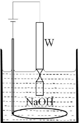
There are several ways to remove native oxide from a silicon surface. One of the simplest techniques is to etch away the oxide layer in dil. hydrofluoric acid (HF). Since the etch rate of oxide in dil. HF is higher than that of the underlying silicon, the oxide layer can be etched without affecting the silicon. This etching process leaves the silicon surface passivated with hydrogen. However, the silicon surface passivated with hydrogen does not last long. The hydrogen bonds on the passivated silicon surface quickly react with oxygen and the oxide layer is regrown. Studies have shown that the hydrogen passivation is replaced with oxygen in less than 30 mins [36]. Furthermore, the hydrogen passivated surface and the residual dangling bonds of a Si dimer, react with hydrocarbons in the air to form two Si-C bonds [37-42]. On annealing, this hydrocarbon contamination forms SiC nanostructures on the silicon surface which severely hinders surface analysis. Therefore, chemical etching of native oxide prior to UHV processing is not a reliable surface cleaning technique for surface analysis.
1.2 Thermal processing of SOI
In ultra-high vacuum (UHV), the native oxide can be removed via a thermal desorption process [43-54]. At high temperatures, silicon dioxide (SiO2) can react
with silicon to form silicon monoxide (SiO) which eventually sublimes as shown by the equation
SiO2 + Si → 2SiO (g)↑ (1.1)
Typically, this process is carried out by heating samples to temperatures over 800 ºC [32, 50, 55]. Sublimation of silicon monoxide from the surface forms voids in the oxide layer which eventually grows in size exposing the silicon beneath [32, 44, 52, 56]. This process removes the native oxide from the sample, resulting
in an atomically clean surface [44, 52, 56]. Chapter 3 presents the challenges
involved in the processing of SOI film without changing its chemical composition on the surface or loss of integrity of the SOI film. The processing parameters and the results of surface analysis are discussed in chapter 3.
6
are not issues in bulk silicon. The following sections briefly discuss some of the
important challenges associated with thermal processing of SOI and SOI
nanostructures and the chapters in which they are discussed in the thesis. 1.3 Formation of SiC surface structures
A clean silicon surface is crucial for surface studies. Thermal processing of silicon results in the removal of native oxide, nevertheless, at high temperatures, silicon also reacts with carbon contaminants and forms SiC structures on the surface according to the equation given by
SiO2 + 3C = SiC + 2CO (1.2)
The carbon contamination usually occurs due to ex situ processing, but the
contamination can also occur due to outgassing of the sample holder and other UHV components at high temperatures.
1.4 Diffusion of dopants
The SOI device layer is actually sandwiched between two SiO2 layers –
buried oxide and native oxide. The presence of fixed charge in the oxide and the traps in the Si-SiO2 interface, can cause the ultra-thin SOI device layer to become
fully depleted of charge carriers [21, 32]. Even for the highest quality Si(100)-BOX interface, the interface trap density is on the order of 1010 - 1011 cm-2 [21, 32, 57].
In contrast, a 45 nm device layer doped at a typical 1015 cm-3 has only 1015 × 45
× 10-7 = 4.5 × 10⁹ majority carriers per cm-2. Hence, SOI with device layer
thickness lower than 45 nm (typical thicknesses considered in this study), with nominal doping (1015 cm-3), would be fully depleted of charge carriers. The lack of
charge carriers in the film makes it difficult to carry out electrical transport measurements in fully depleted SOI [32, 57], especially at low temperatures. Therefore, in order to conduct surface analysis of SOI structures using STM, the device layer of SOI is doped over 1019 cm-3.
High temperature processing of doped silicon leads to diffusion of dopants
7
within the device layer [61-63]. Dopant segregation and clustering can significantly affect the electrical properties of the SOI film and nanostructures [61-63]. Details about diffusion of dopants and varying electrical properties are discussed in chapter 4.
1.5 Spreading resistance
A small area electrical contact (such as that associated with STM) results in an additional series resistance called the spreading resistance which arises due to the spreading of the current from the contact region. Spreading resistance was first explained by Maxwell in 1904 [64]. In this case, most of the voltage drops near the contact where the current density is
the highest and the current density and hence the resistance approaches zero far from the contact. A schematic of current density in a semiconductor from a circular metal contact with radius 𝑎 is shown in Fig. 3. The brown lines in Fig. 3 shows the
current lines and the blue lines show the equipotential surface for the current flowing through the circular contact. The equipotential surfaces in the contact consists of an ellipsoid defined by the equation
𝑟2 𝑎2 + 𝜇2+
𝑧2 𝜇2 = 1
(1.3)
Where μ is the length of the vertical semi-axis of the ellipsoid and (r, z) are the
cylindrical coordinates. The resistance between the equipotential surface with semi-axis μ and the contact is given as [65]
8
𝑅𝜇 = 𝜌 2𝜋∫
𝑑𝜇 (𝑎2+ 𝜇2)=
𝜌 2𝜋𝑎
0
𝑡𝑎𝑛−1(𝜇 𝑎)
(1.4)
where 𝜌 is the resistivity of the semiconductor. Sufficiently far away from the
contact where μ is large, the spreading resistance is given by
𝑅𝑠 = 𝜌
4𝑎 (1.5)
As the relation above suggests, spreading resistance increases with decreasing contact radius. Hence, the contribution of the spreading resistance can become significant in the small contacts formed by scanning probe microscopy based electrical measurements like conductive-atomic force microscopy (C-AFM). Spreading resistance profiling (SRP), a modified C-AFM technique, has become a widely used resistivity and carrier concentration profiling technique [66, 67].
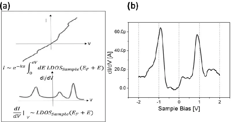
In an STM, an atomically sharp metallic tip is used to analyse a conducting sample. The tunneling contact radius in a typical STM measurement is on the order of 0.5 – 1.5 nm. In normal operation, the tunneling resistance, which is about 10 – 100 GΩ, dominates as the sample resistance and spreading resistance are negligible
in comparison. The dominance of tunneling resistance ensures the voltage drop to occur at the tunneling point, hence enabling an accurate determination of the energy states of the sample surface. However, for samples with high resistivity, spreading resistance can become significant in STM measurements [68] and shifts in spectral features can be observed. However, if these shifts can be modelled, STM and STS may be used to determine the carrier concentration of the sample, similar to SRP [56].
9
1.6 Dewetting
At high temperatures, the thin device layer of SOI can become mechanically unstable and the thin film can break up into 3D crystals [3, 23, 69-71]. This process is driven by surface energy minimization and occurs well below the melting temperature of the film [3]. The Si film in SOI has a higher surface energy than the oxide underneath. Therefore, at elevated temperatures, once the native oxide has been removed, the system tries to minimize the surface energy by exposing the lower surface energy BOX and forming silicon 3D crystals with a reduced surface area. The driving force for dewetting and the rate of dewetting, both increase with decreasing film thickness. As a consequence, thinner films tend to dewet at lower temperature.
Since thin films are usually metastable, they often tend to become unstable and evolve into equilibrium morphologies when they are heated to sufficiently high temperatures. The equilibrium morphology is either a flat film or a hemispherical island, depending on the relative magnitude of the surface energy of the film (𝛾𝐿𝑉),
surface energy of the substrate (𝛾𝑆𝑉), and the interfacial energy of the film and the
substrate (𝛾𝑆𝐿). The expression [72] for the thermodynamic equilibrium between
the three phases is given by,
𝛾𝑆𝑉 = 𝛾𝑆𝐿+ 𝛾𝐿𝑉cos 𝜃 (1.6)
where 𝜃 is the equilibrium contact angle at the three-phase boundary. When 𝛾𝑆𝑉 ≥ 𝛾𝑆𝐿+ 𝛾𝐿𝑉, 𝜃 is 0º, meaning that the film wets the substrate and remains flat and
continuous. However, when 𝜃 is nonzero, the equilibrium morphology of the film
tends to shift from a flat continuous film to a hemispherical island, as shown in Fig. 1.4.
10
There are two different mechanisms through which a 2D film can agglomerate into crystals. Dewetting can occur through the propagation of nucleated voids or through spontaneously growing thermal fluctuations. In the first mechanism, the dewetting process is initiated by the presence of voids on the crystalline SOI film. However, analysis of the energetics of SOI films have shown that the film is stable against small morphology perturbations [73, 74], and the activation energy required to form even a small void in a very thin SOI film is prohibitively large [3]. Therefore homogeneous spontaneous nucleation of voids does not occur. The nucleation of the void in SOI is believed to occur only at defect sites on the surface or the interfaces of the film [75-77]. Hence, it is heterogeneous in nature and enabled by intrinsic defects in the film. The defects may include dislocations, stacking faults, oxide precipitates, surface particles, protrusions on the BOX or scratches in the film induced during SOI processing [76, 77]. Also, in order for the voids to grow, the size of the void must exceed a critical size (rvoid>rcrit). Once supercritical voids are formed in the film, they grow in size via
different morphological instabilities such as surface diffusion induced edge instability and Rayleigh instability.
For extremely thin films, dewetting occurs through the amplification of surface waves [78]. A competition between the stabilizing effect of interfacial tension and attractive intermolecular forces between the substrate and film-vacuum interfaces drives the thickness fluctuations in the film. The amplitude of the perturbations grows with time and eventually leads to dewetting if the growth in the amplitude lowers the total energy of the system. Otherwise, the perturbation decays and the film remains intact. Van der Waals forces become significant in the ultra-thin films which can overcome the interfacial tension, leading to spontaneous amplification of the thickness fluctuations which can eventually dewet the film [78-81] and contact angles that are not well described by the macroscopic Young’s equation (1.6).
11
identified. It is shown in this chapter that the mechanism of thermal instability and dewetting of SOI below 4 nm deviates from thicker SOI.
1.7 Capillary-induced surface diffusion
Sharp edges of structures fabricated on silicon are fundamentally unstable at high temperatures due to their high local surface curvature [3]. The change in curvature creates a free-energy gradient that drives diffusion of atoms away from the curvature towards the flat region [3, 82-84]. This process further leads to capillary edge instability. At high temperatures, the increased diffusion at the edges of SOI thin films and nanostructures fabricated with SOI, can cause the device layer to peel back and uncover the BOX. This effect at the edges enables both oxide desorption and dewetting to occur at lower temperature.
The propagation of mass flow and subsequent dewetting at the void edge is due to surface-energy-driven surface-diffusion-induced morphological instability [3, 85, 86]. This instability is primarily dependent on the temperature and thickness of SOI. Assuming surface energies to be isotropic, the equation for the volumetric surface flux (i.e. volume flux along a surface per unit length perpendicular to the flux) due to surface-energy-driven surface diffusion is given by
𝐽𝑠 = − 𝐷𝑠𝛾Ω
2𝑣
𝑘𝑇 ∇𝜅(𝑠)
(1.7)
Where 𝐷𝑠 is the surface diffusivity, 𝛾 is the surface energy, Ω is the atomic volume,
𝑣 is the atomic surface density, 𝜅(𝑠) is the mean surface curvature along the surface
coordinate 𝑠, 𝑘 is the Boltzmann constant, and 𝑇 is the absolute temperature [3].
The atomic surface diffusion along the surface of the film is determined by the mean surface curvature profile of the film, driving mass flow from regions of higher mean curvature to lower mean curvature [3]. Since, 𝐷𝑠 has a strong positive
Arrhenius temperature dependence, (𝐷𝑠 = 𝐷0exp (− 𝑄𝑠⁄𝑘𝑇), where 𝐷0 is the
surface diffusion pre-exponential factor and 𝑄𝑠 is the activation energy for surface
12
The film thickness dependency of the film edge instability can be understood from the geometrical argument outlined below. Fig. 1.5, shows that for an edge in the SOI device layer, the surface curvature (𝜅𝑒𝑑𝑔𝑒~ 𝑟𝑒𝑑𝑔𝑒−1) is approximately 𝑡𝑆𝑖−1
and the surface distance of the curvature Δ𝑠𝑒𝑑𝑔𝑒 is approximately equals a quarter
arc of a circle given by 𝜋𝑡𝑆𝑖⁄2. Therefore, the average local curvature gradient can
be approximated by
∇𝜅(𝑒𝑑𝑔𝑒) ~ Δ𝜅(𝑒𝑑𝑔𝑒) Δ𝑠𝑒𝑑𝑔𝑒 ~
1 𝑡⁄ 𝑆𝑖 𝜋𝑡𝑆𝑖⁄2 ~
2 𝜋
1 𝑡𝑆𝑖2
(1.8)
From (1.7) and (1.8), local surface diffusion flux at the film edge, 𝐽𝑠, has a inverse
square dependence on Si film thickness, consistent with the existence of a capillary edge instability that drives the retraction of SOI edges. It also shows that edge instability increase rapidly with decreasing film thickness and increasing temperature [3].
1.8 Rayleigh Instability
13
rods [90].The characteristic wavelength of the Rayleigh instability is proportional to the original radius 𝑅𝑐𝑦𝑙 of the cylinder and independent of the temperature.
A high aspect ratio nanowire fabricated with SOI breaks into crystals whose size increases proportionally to the initial radius of the nanowire. The evolution timescale of the Rayleigh instability decreases with the radius of the wire and also decreases strongly with increasing temperature. Therefore thinner nanowires break at lower temperature.
[image:29.595.138.478.131.349.2]Due to the capillary edge and Rayleigh instabilities, nanowires fabricated from SOI dewets at a reduced temperature compared to un-patterned SOI, and therefore makes the surface analysis of nanowires challenging. However, it is shown in chapter 6 that the very forces that destabilises and deforms the nanowires could be used to clean the nanowires by controlling the thermal processing conditions. In this chapter, we have shown that surface analysis through STM can be conducted on ultra-small silicon nanowires on insulator structures. Furthermore, as a basis for future work, a simple nanowire and nanodisc fabrication technique has been demonstrated.
14 1.9 References
1. Teich, M.C. and B. Saleh, Fundamentals of photonics. Canada, Wiley Interscience, 1991. 3.
2. Bhat, N., Nanoelectronics Era: Novel Device Technologies Enabling Systems on Chips. Journal of the Indian Institute of Science, 2012. 87(1): p. 61.
3. Danielson, D.T., et al., Surface-energy-driven dewetting theory of silicon-on-insulator agglomeration. Journal of Applied Physics, 2006. 100(8): p. 083507. 4. Berg, J.A.V.d., et al., Characterization by medium energy ion scattering of
damage and dopant profiles produced by ultrashallow B and As implants into Si at different temperatures. Journal of Vacuum Science & Technology B: Microelectronics and Nanometer Structures Processing, Measurement, and Phenomena, 2002. 20(3): p. 974-983.
5. Riss, A., et al., Local Electronic and Chemical Structure of Oligo-acetylene Derivatives Formed Through Radical Cyclizations at a Surface. Nano Letters, 2014. 14(5): p. 2251-2255.
6. Schaller, R.R., Moore's law: past, present and future. IEEE spectrum, 1997. 34(6): p. 52-59.
7. Moore, G.E. Progress in digital integrated electronics. in Electron Devices Meeting. 1975.
8. Bohr, M. and K. Mistry, Intel’s revolutionary 22 nm transistor technology. Intel website, 2011.
9. Doyle, B., et al., Transistor Elements for 30nm Physical Gate Lengths and Beyond. Intel Technology Journal, 2002. 6(2).
10.Ko, H., et al., Ultrathin compound semiconductor on insulator layers for high performance nanoscale transistors. arXiv preprint arXiv:1108.1127, 2011. 11.Lyons, D.M., et al., Tailoring the Optical Properties of Silicon Nanowire Arrays
through Strain. Nano Letters, 2002. 2(8): p. 811-816.
15
13.Hodes, G., When Small Is Different: Some Recent Advances in Concepts and Applications of Nanoscale Phenomena. Advanced Materials, 2007. 19(5):p.639-655.
14.Wilson, W.L., P. Szajowski, and L. Brus, Quantum confinement in size-selected, surface-oxidized silicon nanocrystals. SCIENCE-NEW YORK THEN WASHINGTON-, 1993. 262: p. 1242-1242.
15.Wu, Z., J.B. Neaton, and J.C. Grossman, Quantum Confinement and Electronic Properties of Tapered Silicon Nanowires. Physical Review Letters, 2008. 100(24): p. 246804.
16.Leão, C.R., A. Fazzio, and A.J.R. da Silva, Si Nanowires as Sensors: Choosing the Right Surface. Nano Letters, 2007. 7(5): p. 1172-1177.
17.Jang, H., et al., Quantum Confinement Effects in Transferrable Silicon Nanomembranes and Their Applications on Unusual Substrates. Nano Letters, 2013. 13(11): p. 5600-5607.
18.Nolan, M., et al., Silicon nanowire band gap modification. Nano letters, 2007. 7(1): p. 34-38.
19.Hirschman, K., et al., Silicon-based visible light-emitting devices integrated into microelectronic circuits. Nature, 1996. 384(6607): p. 338.
20.Pavesi, L., et al., Optical gain in silicon nanocrystals. Nature, 2000. 408(6811): p. 440.
21.Zhang, P., et al., Electronic transport in nanometre-scale silicon-on-insulator membranes. Nature, 2006. 439(7077): p. 703.
22.Lu, Z., et al., Quantum confinement and light emission in SiO2/Si superlattices.
Nature, 1995. 378(6554): p. 258.
23.Legrand, B., et al., Formation of silicon islands on a silicon on insulator substrate upon thermal annealing. Applied Physics Letters, 2000. 76(22): p. 3271.
24.Liu, F., Self-Assembly of Three-Dimensional Metal Islands: Nonstrained versus Strained Islands. Physical Review Letters, 2002. 89(24): p. 246105.
16
26.Sun, J. and S.L. Simon, The melting behavior of aluminum nanoparticles. Thermochimica Acta, 2007. 463(1): p. 32-40.
27.Guisbiers, G., et al., Mechanical and thermal properties of metallic and semiconductive nanostructures. The Journal of Physical Chemistry C, 2008. 112(11): p. 4097-4103.
28.Yakunin, A.M., et al., Warping a single Mn acceptor wavefunction by straining the GaAs host. Nature Materials, 2007. 6: p. 512.
29.Wijnheijmer, A.P., et al., Enhanced Donor Binding Energy Close to a Semiconductor Surface. Physical Review Letters, 2009. 102(16): p. 166101. 30.Georgiev, V.P., et al., Experimental and Simulation Study of Silicon Nanowire
Transistors Using Heavily Doped Channels. IEEE Transactions on Nanotechnology, 2017. 16(5): p. 727-735.
31.Teo, B.K. and X.H. Sun, Silicon-Based Low-Dimensional Nanomaterials and Nanodevices. Chemical Reviews, 2007. 107(5): p. 1454-1532.
32.Sutter, P., W. Ernst, and E. Sutter, Scanning tunneling microscopy on ultrathin silicon on insulator (100). Applied Physics Letters, 2004. 85(15): p. 3148. 33.Celler, G. and S. Cristoloveanu, Frontiers of silicon-on-insulator. Journal of
Applied Physics, 2003. 93(9): p. 4955-4978.
34.Yan, R.-H., A. Ourmazd, and K.F. Lee, Scaling the Si MOSFET: From bulk to SOI to bulk. IEEE Transactions on Electron Devices, 1992. 39(7): p. 1704-1710. 35.Flandre, D., et al., Fully-depleted SOI CMOS technology for voltage
low-power mixed digital/analog/microwave circuits. Analog Integrated Circuits and Signal Processing, 1999. 21(3): p. 213-228.
36.Zhao, L., et al., Characterization on the passivation stability of HF aqueous solution treated silicon surfaces for HIT solar cell application by the effective minority carrier lifetime measurement. Chinese Journal of Physics, 2010. 48(3): p. 392-399.
37.Bender, H., S. Verhaverbeke, and M. Heyns, Hydrogen Passivation of HF‐Last
17
38.Mayne, A.J., et al., An STM study of the chemisorption of C2H4 on Si(001)(2 ×
1). Surface Science, 1993. 284(3): p. 247-256. 39.Bozack, M.J., et al.,
Surface Science, 1986. 177(1): p. L933-L937.
40.Pan, W., T. Zhu, and W. Yang, First-principles study of the structural and electronic properties of ethylene adsorption on Si(100)-(2×1) surface. The Journal of Chemical Physics, 1997. 107(10): p. 3981-3985.
41.Fisher, A.J., P.E. Blöchl, and G.A.D. Briggs, Hydrocarbon adsorption on Si(001): when does the Si dimer bond break? Surface Science, 1997. 374(1): p. 298-305. 42.Yoshinobu, J., et al., The adsorbed states of ethylene on Si(100)c(4×2), Si(100)(2×1), and vicinal Si(100) 9°: Electron energy loss spectroscopy and low‐energy electron diffraction studies. The Journal of Chemical Physics, 1987.
87(12): p. 7332-7340.
43.Barimar, P.S.N., et al., Study of the effect of thermal treatment on morphology and chemical composition of silicon-on-insulator. Journal of Vacuum Science & Technology B, Nanotechnology and Microelectronics: Materials, Processing, Measurement, and Phenomena, 2016. 34(4): p. 041806.
44.Xue, K., J.B. Xu, and H.P. Ho, Nanoscale in situ investigation of ultrathin silicon oxide thermal decomposition by high temperature scanning tunneling microscopy. Nanotechnology, 2007. 18(48): p. 485709.
45.Hibino, H., M. Uematsu, and Y. Watanabe, Void growth during thermal decomposition of silicon oxide layers studied by low-energy electron microscopy. Journal of Applied Physics, 2006. 100(11): p. 113519.
46.Johansson, U., H. Zhang, and R. Nyholm, Thermal desorption of oxides on Si(100): a case study for the scanning photoelectron microscope at MAX-LAB. Journal of Electron Spectroscopy and Related Phenomena, 1997. 84(1): p. 45-52.
18
48.Sun, Y.K., D.J. Bonser, and T. Engel, Thermal decomposition of ultrathin oxide layers on Si(100). Journal of Vacuum Science & Technology A: Vacuum, Surfaces, and Films, 1992. 10(4): p. 2314-2321.
49.Ogawa, S., et al., Consumption kinetics of Si atoms during growth and decomposition of very thin oxide on Si(001) surfaces. Thin Solid Films, 2006. 508(1): p. 169-174.
50.Tromp, R., et al., High-Temperature SiO2 Decomposition at the SiO2/Si
Interface. Physical Review Letters, 1985. 55(21): p. 2332-2335.
51.Johnson, K.E. and T. Engel, Direct measurement of reaction kinetics for the decomposition of ultrathin oxide on Si(001) using scanning tunneling microscopy. Physical Review Letters, 1992. 69(2): p. 339-342.
52.Jones, D. and V. Palermo, Production of nanostructures of silicon on silicon by atomic self-organization observed by scanning tunneling microscopy. Applied Physics Letters, 2002. 80(4): p. 673-675.
53.Kinefuchi, I., et al., Inhomogeneous decomposition of ultrathin oxide films on Si(100): Application of Avrami kinetics to thermal desorption spectra. The Journal of Chemical Physics, 2008. 128(16): p. 164712.
54.Liehr, M., J.E. Lewis, and G.W. Rubloff, Kinetics of high‐temperature thermal
decomposition of SiO2 on Si(100). Journal of Vacuum Science & Technology A:
Vacuum, Surfaces, and Films, 1987. 5(4): p. 1559-1562.
55.Ota, Y., n‐Type Doping Techniques in Silicon Molecular Beam Epitaxy by
Simultaneous Arsenic Ion Implantation and by Antimony Evaporation. J. Electrochem. Soc, 1979. 126(10).
56.Barimar, P.S.N., et al., Spreading resistance at the nano-scale studied by scanning tunneling and field emission spectroscopy. Applied Physics Letters, 2017. 110(26): p. 263111.
57.Lin, K.C., et al., Surface characterization of silicon on insulator material. Applied Physics Letters, 1998. 72(18): p. 2313-2315.
19
59.Zhang, K., et al., Fast flexible electronics using transferrable silicon nanomembranes. Journal of Physics D: Applied Physics, 2012. 45(14): p. 143001.
60.Ndoye, C., T. Liu, and M. Orlowski, Comparison of Diffusion Mechanisms in Si Bulk, Nanomembranes, and Nanowires. ECS Transactions, 2011. 33(31): p. 3-18.
61.Shibahara, K., et al., Dopant loss origins of low energy implanted arsenic and antimony for ultra shallow junction formation. MRS Online Proceedings Library Archive, 1998. 532.
62.Meishoku, K., et al., Quantitative Evaluation of Dopant Loss in 5–10 keV As Ion Implantation for Low-Resistive, Ultrashallow Source/Drain Formation. Japanese Journal of Applied Physics, 1999. 38(4S): p. 2324.
63.Pei, L., Dopant Segregation at Silicon-Oxide Interfaces. 2007.
64.LEVIN, M. and M. MILLER, Maxwell a treatise on electricity and magnetism. Uspekhi Fizicheskikh Nauk, 1981. 135(3): p. 425-440.
65.Slade, P.G., Electrical contacts - principles and applications. second ed.
66.Mazur, R. and D. Dickey, A spreading resistance technique for resistivity measurements on silicon. Journal of the electrochemical society, 1966. 113(3): p. 255-259.
67.Ehrstein, J.R., Spreading resistance measurements—An overview, in Emerging Semiconductor Technology. 1987, ASTM International.
68.Johnson, M.B. and J.M. Halbout, Scanning tunneling microscopy and spectroscopy for studying cross‐sectioned Si(100). Journal of Vacuum Science
& Technology B, 1992. 10(1): p. 508-514.
69.Tabe, M., et al., Formation of high-density silicon dots on a silicon-on-insulator substrate. Applied Surface Science, 1999. 142(1–4): p. 553-557.
70.Bussmann, E., et al., Thermal instability of silicon-on-insulator thin films measured by low-energy electron microscopy. IOP Conference Series: Materials Science and Engineering, 2010. 12: p. 012016.
20
72.Young, T., An essay on the cohesion of fluids. Philosophical Transactions of the Royal Society of London, 1805. 95: p. 65-87.
73.Aouassa, M., et al., The kinetics of dewetting ultra-thin Si layers from silicon dioxide. New Journal of Physics, 2012. 14(6): p. 063038.
74.Srolovitz, D.J. and S.A. Safran, Capillary instabilities in thin films. I. Energetics. Journal of Applied Physics, 1986. 60(1): p. 247-254.
75.Yukinori, O., et al., Thermal Agglomeration of Thin Single Crystal Si on SiO2 in
Vacuum. Japanese Journal of Applied Physics, 1995. 34(4R): p. 1728.
76.D. K. Sadana, J.L., H. J. Hovel, K. Petrillo, and P. Roitman, Proceedings of the 1994 IEEE International SOI Conference (IEEE, Piscataway, NJ, 1994): p. 111. 77.Giles, L.F., A. Nejim, and P.L.F. Hemment, New etchant for crystallographic
defect studies in thin SOI materials (<1000 AA). Electronics Letters, 1993. 29(9): p. 788-789.
78.Singh, S.P., Spinodal theory: A common rupturing mechanism in spinodal dewetting and surface directed phase separation (some technological aspects: Spatial correlations and the significance of dipole-quadrupole interaction in spinodal dewetting). Advances in Condensed Matter Physics, 2011. 2011. 79.Bischof, J., et al., Dewetting Modes of Thin Metallic Films: Nucleation of Holes
and Spinodal Dewetting. Physical Review Letters, 1996. 77(8): p. 1536-1539. 80.Trice, J., et al., Novel self-organization mechanism in ultrathin liquid films:
theory and experiment. Physical review letters, 2008. 101(1): p. 017802. 81.Brada, M. and D. Clarke, A thermodynamic approach to the wetting and
dewetting of grain boundaries. Acta materialia, 1997. 45(6): p. 2501-2508. 82.Mullins, W.W., Flattening of a Nearly Plane Solid Surface due to Capillarity.
Journal of Applied Physics, 1959. 30(1): p. 77-83.
83.Celano, T.A., et al., Capillarity-Driven Welding of Semiconductor Nanowires for Crystalline and Electrically Ohmic Junctions. Nano letters, 2016.16(8):p.5241-5246.
84.Nichols, F. and W. Mullins, Morphological changes of a surface of revolution due to capillarity‐induced surface diffusion. Journal of Applied Physics, 1965.
21
85.Jiran, E. and C.V. Thompson, Capillary instabilities in thin films. Journal of Electronic Materials, 1990. 19(11): p. 1153-1160.
86.Jiran, E. and C.V. Thompson, Capillary instabilities in thin, continuous films. Thin Solid Films, 1992. 208(1): p. 23-28.
87.Peng, H.Y., et al., Bulk-quantity Si nanosphere chains prepared from semi-infinite length Si nanowires. Journal of Applied Physics, 2001. 89(1): p. 727-731.
88.Rauber, M., et al., Thermal stability of electrodeposited platinum nanowires and morphological transformations at elevated temperatures. Nanotechnology, 2012. 23(47): p. 475710.
89.Rayleigh, L., On The Instability Of Jets. Proceedings of the London Mathematical Society, 1878. s1-10(1): p. 4-13.
22
2
E
Q U I P M E N T
&
M
E T H O D S
The principles behind many of the experimental techniques used throughout this thesis are introduced in this chapter including scanning tunneling microscopy, X-ray photoelectron spectroscopy, atomic force microscopy, electron microscopy and lithography techniques.
2. 1 Ultra-high vacuum
Vacuum is generally categorized as low, high and ultra-high vacuum based on the pressure range. Ultra-high vacuum (UHV) is a regime of vacuum which is characterized by a pressure that is lower than 10-9 mbar. Most surface science
studies are carried out in an UHV environment. UHV conditions allow atomically clean surfaces to be obtained and maintained in a contamination free environment during the course of the experiment. Also, some techniques like low energy electron diffraction and X-ray photoelectron spectroscopy need UHV so that electrons can reach the screen or analyser without colliding with particles and being deflected. At atmospheric pressure a gas molecule has a mean free path of ~60 nm, which means that the gas molecule travels only around 60 nm between two collisions, while at UHV, the molecules have a mean free path of several kilometres [13]. This means that in low pressure only a few molecules will contaminate the sample surface. Therefore for surface science experiments that require atomically clean surfaces, UHV conditions are essential.
23
elevated temperature up to 200 ºC, hence refractive metals such as Molybdenum and Tantalum are used in cases of high temperature applications. In order to attain UHV, the whole system is “baked”, i.e. heated up to temperatures above 100 ºC to facilitate desorption of water and contaminants from the inner walls of the chamber. While baking, all parts within the chamber are also heated to temperatures slightly higher than their working temperature to allow desorption of adsorbed gasses which would otherwise outgas during experimental work.
Several different UHV systems have been used for the experiments described in this thesis. While the scanning tunneling microscopy (STM) and X-ray photoelectron spectroscopy (XPS) measurements were carried out with a CreaTec LT-STM/AFM system and a VG Scienta ESCALab MKII system respectively, the thermal process optimization was carried out in a home-made UHV system. Details about the CreaTech LT-STM/AFM and the home-made UHV system will be described in the following section and the VG Scienta ESCALab MKII XPS system will be presented in the XPS section.
2.2 Scanning tunneling microscopy (STM)
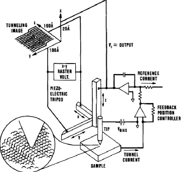
STM is a type of scanning probe microscopy that uses electron tunneling to measure the properties of conducting surfaces with atomic resolution. STM was developed at IBM Zurich in the 1980s by Binning and Rohrer [3, 15, 16] and since then has developed into an important tool in surface science. STM operates on the principle of quantum mechanical tunneling: when a metallic tip is brought to within several angstroms from a surface and a bias is applied, there is a finite probability that electrons will tunnel between the tip and the surface. The direction of the tunneling depends on the applied bias. STM probes the local electronic density of states of the surface, allowing investigation of surface reconstruction and surface defects at the atomic scale. To a first approximation, STM provides information on the topography of the surface[17].
24
mechanics, an electron is described with a wave function 𝜓(𝑥) which satisfies the
Schrödinger equation:
− ħ
2
2𝑚 𝑑2
𝑑𝑥2𝜓(𝑥) + [𝑉(𝑥)−𝐸]𝜓 = 0
(2.1)
Fig. 2.1 shows the wave function of an electron with energy E interacting with a one-dimensional potential barrier of height Vo and width s. In Region 1 where E >
Vo Equation (1) has the solution
𝜓(𝑥) = 𝜓(0)𝑒±𝑖𝑘𝑥 (2.2)
where
𝑘 = √(2𝑚 (𝐸−𝑉𝑜) ћ
(2.3)
Where 𝑚 is the mass of the electron, ћ is Planck’s constant divided by 2π and 𝑘
represents a travelling wave [5]. In Region 2 where E < Vo, the solution is of the
form
𝜓(𝑥) = 𝜓(0)𝑒±𝛼𝑥 (2.4)
where
𝛼 = √(2𝑚 (𝑉𝑜− 𝐸) ћ
(2.5)
α is known as the decay constant [5]. In Region 3 (E > Vo) the solution is
𝜓(𝑥) = 𝜓(0)𝑒−𝛼𝑥 (2.6)
V
s
E > Vo
E
E < Vo E > Vo Vo
1 2 3
Fig. 2.1: Wave function 𝜓(𝑥) for an electron with energy E interacting with a one
dimensional potential barrier with height Vo and width s. Within the classically forbidden Region 2 (E < Vo), the wave function decays exponentially and is present in Region 3 (E
25
Hence the electron wave function decays exponentially within the barrier and for a sufficiently narrow barrier, there is a finite probability that the particle will tunnel through the barrier. The probability density P of the wavefunction tunneling through the barrier is proportional to the square of the wave function [18] (2.6),
𝑃 ∝ |𝜓(0)|2𝑒−2𝛼𝑥 (2.6 (a))
2.2.2 Elastic tunneling through a one-dimensional potential barrier of arbitrary shape
An extension to the potential barrier of arbitrary shape can be obtained from the description outlined in the section above using the Wentzel-Kramers-Brillouin (WKB) approximation [17]. The WKB approximation is based on treating Planck’s constant (6.626×10⁻³⁴ m2 Kg s-1) as a small number. The expression of the
probability D(E) of an electron tunneling through a barrier of arbitrary shape is given by
Where 𝑉(𝑥) is the barrier height at any position 𝑥, 𝑠1 and 𝑠2 (refer to Fig. 2.2) are
the classical turning points of the barrier and Δ𝑠 = (𝑠2− 𝑠1) is the width of the
barrier. The WKB approximation is appropriate only if 𝐸 ≪ 𝑉 and the slope of
either side (𝑠2 and 𝑠1) of the barrier is gentle.
2.2.3 Elastic tunneling in planar metal-insulator-metal (MIM) tunnel junctions
The illustration of elastic tunneling in a one-dimensional potential barrier can be applied to MIM tunnel junctions as shown in Fig. 2.2. Here we consider similar metal electrodes at thermal equilibrium, exhibiting free electron behavior. The insulator is treated as though it were a vacuum. From Eq. (2.7), for an electron with energy component 𝐸𝑥 with
𝐸𝑥 = (𝑚𝑣𝑥
2)
2
(2.8)
where 𝑣𝑥 is the electron velocity component in 𝑥 and m is the electron mass, the
probability 𝐷(𝐸𝑥) of the electron tunneling from one electrode to another through
an arbitrary shaped barrier is given by
𝐷(𝐸) = exp(−2
ħ ∫ √2𝑚 [𝑉(𝑥) − 𝐸]
𝑠2
𝑠1
𝑑𝑥)
= exp( −2 ∫ 𝛼(𝑥, 𝐸) 𝑑𝑥)
𝑠2
𝑠1
26
𝐷(𝐸𝑥) = exp(−2√2𝑚
ħ ∫ √[𝜂 + 𝜙(𝑥) − 𝐸𝑥]
2
𝑠1
𝑑𝑥) (2.9)
where 𝑆1 and 𝑆2 are the distances from the surface of Electrode 1 to the point
where the potential energy equals the Fermi energy near electrode surfaces 1 and 2 as shown in Fig. 2.2, 𝜂 is the Fermi level of the electrode 1 and 𝜙(𝑥) is the
potential energy of an electron at any position 𝑥 between the two surfaces. By
introducing a term ϕ [9] , defined as mean potential barrier height 𝜙 above the
Fermi level 𝜂 where
ϕ = 1
Δ𝑠 ∫ 𝜙(𝑥) 𝑑𝑥 𝑠2
𝑠1
the tunneling current density 𝐽 at 0 K can be expressed as:
𝐽 = 𝐽0 ϕ exp (−𝐴Δ𝑠√ ϕ ) − 𝐽0( ϕ + eV) exp(−𝐴Δ𝑠√ ϕ + eV) (2.10)
where
𝐽0 =
𝑒
4𝜋2ħ(𝛽Δ𝑠)2 , A =
2β√2𝑚
ħ , 𝛽 ≈ 1
Here, eV is the potential between the two electrodes. Eq. (2.10) can be interpreted as a current density J1 flowing from Electrode 1 to Electrode 2 and a current density
𝑱𝟏 𝑱𝟐
Fermi Level
V
eU Fermi Level
[image:42.595.142.438.488.701.2]ELECTRODE 1 INSULATOR ELECTRODE 1 Vacuum level
27
J2 flowing from Electrode 2 to Electrode 1, with the difference between them equal
to the net density J. The current density is zero with no voltage applied. With an applied voltage, the barrier is perturbed and this leads to a current flow which is proportional to the applied bias. The applied bias opens up an energy window of allowed states with width equal to eV for tunneling [9].
2.2.4 Quantum mechanical tunneling as applied to STM
An STM basically constitutes a metal or a metal-insulator-conductor system where a metallic tip is separated a small distance s from the conducting sample. The quantum tunneling model for a one dimensional tunnel barrier demonstrated above can be applied to STM and used to calculate the exponential dependence of the tunnel current on tip-sample separation. The tunneling current I typically increases by an order of magnitude for a 1 Å decrease in the tip-sample separation [17-20]. This sensitivity of the tunneling current to tip-sample separation allows the STM to attain atomic resolution.
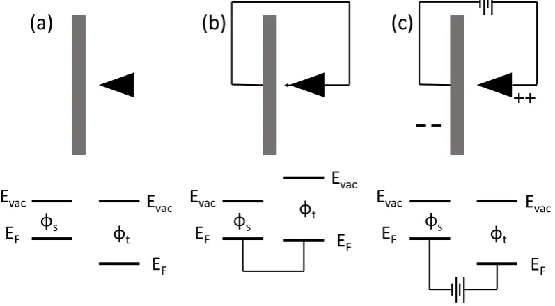
While the analysis of a one-dimensional tunnel barrier describes the exponential dependency of the tunnel current on the tip-sample separation, the scanning tunneling microscope is not one-dimensional. In addition to moving the scanner in the x-y plane with respect to the surface, it is also possible to generate images and spectra through varying the scanner position with respect to the surface in z. A more detailed theoretical treatment of the tunneling current in STM was developed by Bardeen in 1961 [21]. The theory is based on the tunneling process in a metal/insulator system. It is assumed that the metal electrodes are a weakly interacting system in which the tunneling process is facilitated by the overlapping of the wave functions within the insulator, as shown in Fig. 2.3. An expression of the tunneling current was obtained using the time dependent perturbation theory and Fermi’s golden rule [22]. Tersoff and Hamann [11, 23] later extended the approach to provide a quantitative theory for vacuum tunneling between a real solid and a model probe with a spherical tip, as present in the STM. For the case of low temperature (T ≈ 0 K) and small voltage, they obtained an expression for
28
𝐼 = 2𝜋 ħ 𝑒
2𝑉 ∑ |𝑀
𝜇,𝜈|2 𝛿(𝐸𝜇 − 𝐸𝐹)𝛿(𝐸𝑣− 𝐸𝐹) 𝜇,𝑣
(2.11)
where 𝐸𝜇and 𝐸𝐹 are the energies for the states 𝜓𝜇 of the sample and 𝜒𝑣 of the tip,
relative to the Fermi level of the respective electrodes. 𝑀𝜇,𝜈 is the tunneling matrix
element between the two states. The expression (2.11) can be interpreted in a simple fashion by considering the ideal case where the tip is assumed to be a single point charge at 𝑟⃗𝑡𝑖𝑝 with a radius R. In this case the angle dependence of the charge
distribution can be neglected. The tunneling matrix element 𝑀𝜇,𝜈 is then simply
proportional to the amplitude of the sample wave function 𝜓𝜇at 𝑟⃗𝑡𝑖𝑝. In this limit,
Eq. (2.11) can be expressed as
𝐼 (𝑟⃗𝑡𝑖𝑝, 𝑉) ∝ ∑ |𝜓𝜇(𝑟⃗𝑡𝑖𝑝)|2 𝛿(𝐸𝜇− 𝐸𝐹) ≡ 𝜌(𝑟⃗𝑡𝑖𝑝, 𝐸𝐹)
𝜇
(2.12)
The quantity, 𝜌(𝑟⃗𝑡𝑖𝑝, 𝐸𝐹), is the surface local density of states (LDOS) of the sample
surface at 𝐸𝐹 at the position of the tip 𝑟⃗𝑡𝑖𝑝. Thus Eq. (2.12) demonstrates that the
[image:44.595.199.450.412.719.2]STM image is a contour map of constant surface LDOS.
29 2.2.5 STM – Experimental details
Fig. 2.4 shows a schematic diagram of the basic operation of an STM. An atomically sharp metallic tip is scanned over a conducting sample surface with a separation distance of a few ångströms while a potential difference is applied between the tip and the sample. The tip is positioned and scanned over the sample using a piezoelectric actuator which has a typical lateral (x-y) resolution of 0.1 Å and a vertical (z) resolution better than 0.01 Å. In order to achieve sub-ångström precision in an STM, several methods are used to eliminate or reduce mechanical vibration. A number of vibration isolation techniques are used in order to damp
[image:45.595.142.510.282.626.2]![Fig. 1.6: Graphical illustration of the Rayleigh instability. A cylindrical object undulates and transforms into a chain of spheres (image taken from [5])](https://thumb-us.123doks.com/thumbv2/123dok_us/8799716.913440/29.595.138.478.131.349/graphical-illustration-rayleigh-instability-cylindrical-undulates-transforms-spheres.webp)
![Fig. 2.2: Arbitrary shaped potential barrier between two metal electrodes. (Figure taken from [9])](https://thumb-us.123doks.com/thumbv2/123dok_us/8799716.913440/42.595.142.438.488.701/arbitrary-shaped-potential-barrier-metal-electrodes-figure-taken.webp)
![Fig. 2.3: Illustration of the Bardeen approach to tunneling theory [5].](https://thumb-us.123doks.com/thumbv2/123dok_us/8799716.913440/44.595.199.450.412.719/fig-illustration-bardeen-approach-tunneling-theory.webp)

![Fig. 2.16: The phase lag changes depending on the mechanical properties of the sample surface (Image from [6])](https://thumb-us.123doks.com/thumbv2/123dok_us/8799716.913440/58.595.156.436.441.681/phase-changes-depending-mechanical-properties-sample-surface-image.webp)