Digitally Programmable Voltage-Mode Universal
Biquadratic Filter
Mohd. Zihaib Khan
Department of Electronics Engineering Aligarh Muslim University
Aligarh, India
Mohd. Samar Ansari
Department of Electronics EngineeringAligarh Muslim University Aligarh, India
ABSTRACT
A single input multi-output voltage mode universal biquadratic filter has been presented. The circuit incorporates digital programmability employing three plus-type differential voltage current conveyors (DVCCs), two grounded capacitors and three resistors. The circuit exhibits high input impedance realizes all the standard filter functions having orthogonal control of cut-off frequency and quality factor. Parameter tunability is achieved by the use of a 3–bit digital control word. The proposed circuits are amenable for monolithic integration by virtue of the fact that only grounded capacitors are employed. Circuit simulations using PSPICE are in perfect agreement with the theoretically predicted results.
General Terms
Digitally Programmable, Universal Biquadratic Filter.
Keywords
Digital Control, Digitally Controlled Differential Voltage Current Conveyor, DC-DVCC, Programmable Circuits.
1.
INTRODUCTION
There has been a myriad of applications that involve realization of active transfer functions employing current conveyors, which have received a considerable amount of research attention [1].The continuous-time analog filter is a ubiquitous circuit component in a vast variety of applications including, but not limited to, noise rejection & signal separation in industrial and measurement circuits, feedback of phase & amplitude control in servo loops, smoothing of digitally generated analog signals, audio signal shaping & sound enhancement, channel separation & signal enhancement in communication electronics [1]–[14].
Active filter design generally employs one (or more) active building block and passive components like capacitors and resistors; inductors being avoided due to their incompatibility with the standard CMOS fabrication process. The active element may be one of the following: operational amplifier, second generation current conveyor (CCII) [9], operational trans-conductance resistance amplifier (OTRA) [8], fully differential current conveyor (FDCCII) [4], third generation current conveyor (CCIII) [11], differential voltage current conveyor(DVCC) [5],[6], [10], [12]. Circuit design using each of these building blocks has its own associated advantages and limitations with the DVCC offering the highest amount of flexibility and simplicity in analog electronic circuit design.
Voltage-mode active filters exhibiting high input impedance are of great interest as a number of cells can be easily cascaded for the realization of the higher order filters. However, it needs to be mentioned that the advantage of easy cascading can only be obtained in voltage-mode active filters which exhibit high input impedance [2-3].In this paper, digitally programmable DVCC-based implementations for voltage-mode universal biquadratic filter has been presented.
which enhances the circuit utility in terms of its usage and reducing the overall cost of the circuit.
This paper is organized as follows. Section 2 presents a brief review of existing works on the realization of active filters. Section 3 contains an explanation of the operation of the Digitally-Controlled DVCC (DC-DVCC).Section 4 deals with details of the proposed universal biquadratic filter along with the design equations. Section 5 presents the results of computer simulations of the proposed circuit using PSPICE program. Some concluding remarks appear in section 6.
2.
EXISTING METHODS
Analog filter design using a variety of active building blocks has been an active area of research for the past two decades. Operational amplifier was the active element of choice during the earlier stages of development. Later, the advent of current conveyors signaled the era of mixed-mode and current-mode signal processing. Since there has been a significant amount of technical literature available on the subject, it is not possible to attempt a thorough review of all the related works. Therefore, a survey of some of the recently published works is presented in this section. The DVCC was introduced by Elwan & Soliman and its application in continuous-time filters was also discussed [10]. Adawy, Soliman & Elwan later proposed another analog building block viz. the Fully Differential Current Conveyor (FDCCII) and several applications in electronic filters were also presented [7].One significant feature of the filters designed using FDCCII was the possibility of obtaining fully-differential processing. Cakir, Cam & Cicekoglu put forward an all-pass configuration employing a single OTRA [8]. Minaei & Ibrahim employed the DVCC for implementing a general topology for obtaining current-mode first-order APF [12]. A third-generation current conveyor (CCIII) was utilized to yield a trans-admittance type first-order filter [11]. Chiu et al. reported voltage-mode universal biquadratic filter simultaneously realizing all the standard functions all-pass, high-pass, band-pass, band-reject and low-pass filter sections based on DVCC, which forms the background for the present work. [13]. Minaei & Ibrahim presented a mixed-mode universal filter based on the KHN-biquad topology employing DVCCs [11]. Another voltage-mode all-pass filter using DVCC as the building block is attributed to Minaei & Yuce [5]. More recently, Maheshwari et al. used the FDCCII to realize cascadable all-pass/notch filters employing only grounded capacitors as the passive elements [4].
Fig. 2. CMOS implementation of DVCC (asdfgh, 2009)
Fig. 1. Electrical symbol of DC-DVCC[14]
However, when it comes to applications demanding differential or floating inputs like impedance converters and quadrature oscillators which require two highinputimpedance terminals, a single CCII is not generally sufficient. To overcome this shortcoming, the Differential Voltage Current Conveyor (DVCC) was first introduced by Pal, and later developed by Elwan&Soliman[8].The DC-DVCC, shown in Fig.1,is essentially a 5-terminal block defined by the following relations:
While the voltage on the X-terminal follows the difference in voltages of terminals Y1 and Y2, a current injected at the X-terminal is replicated by a factor kto the Z-X-terminals. For the Z+ terminal, the direction of the conveyed current is the same as that of the current flowing in the X-terminal whereas for the Z- terminal, the current flows in the opposite direction. Ideally, k is unity. One possible CMOS realization of the
[image:2.595.315.544.76.211.2]DVCC is shown in Fig. 2 [14]. As can be seen, the current at Z+ port will be the same as the current in the X terminal and the current at the Z-terminal will have the same magnitude but opposite direction as the X port current. To obtain a digitally controlled DVCC (DC-DVCC) from a DVCC, the technique is to control the current transfer gain parameter k of the DVCC by replacing the Z terminal transistors of the DVCC with transistor arrays associated with switches [13]. The gain parameter k can take values from 1 to (2n– 1), where n represents the number of transistor arrays.
Fig. 3. CMOS realization of Digitally Controlled DVCC with gain k[14]
Actually, the transistor arrays implementa current summing network (CSN) at the Z terminal. Thecircuit of DC-DVCC obtained after suitable modifications inthe circuit of Figure 2 is presented in Figure 3 [13]. The CSNconsists of n transistor pairs, whose NMOS and PMOS aspectratios are given by:
PMOS ( ) ( ) (2)
NMOS ( ) ( )
(3)
Therefore, the current at the Z terminal, assumed flowing outof the DC-DVCC, can be expressed by
∑ ( )
(4)
Therefore, the proposed DC-DVCC provides a current transfer gain equal to:
∑ ( )
( ) ∑
(5)
Parameter di represents the digital code-bit applied to the i-th
branch in the CSN. Depending upon its value, it enables or disables the current to flow in that particular branch. It isinstructive to note the numbering of the transistors in the CSN.Transistors labeled M8 (i)and M12 (i)refer to the PMOS
andNMOS transistors in the CSN that have been put there in theplace of their counterparts of Fig. 2.. Transistors MD8
(i)andMD12 (i)are the actual digital control transistors as the
digitalcontrol bits d0, d1and d2are applied at their respective
gateterminals
4.
PROPOSED CIRCUITS
This section presents the proposed DVCC-based voltage-mode universal biquadratic continuous-time filters with electronic control of filter parameters viz.gain and cut-off frequency. The circuit implementation employing DC-DVCC has been depicted in Fig. 4.The circuit has an advantage of using grounded capacitors that makes it feasible for integrated circuit implementation. The circuit has single input multi output configurations realizing all the standard filter functions i.e. low pass, high pass, band pass, band-reject and all-pass filter.
[
]
[
][
]
[image:2.595.93.253.234.353.2] [image:2.595.133.275.571.629.2]The expression for the filter functions can be expressed as: Low Pass (LPF) (6) Band Pass (BPF) (7) Band Reject (BRF) (8) High Pass (HPF) (9) All Pass (APF) (10)
From equations (6) through (10) it can be seen that a low-pass response is obtained from VOUT1, a band-pass response is obtained from VOUT2, a notch response is obtained from VOUT3, a high-pass response is obtained from VOUT4, and if R1
=R3, all-pass response is obtained from VOUT5. The resonant
angular frequency,ωo, and the quality factor, Q, are given by:
Cut-off
Frequency: √ (11)
Quality
Factor: √ (12)
Thus, the proposed circuit is capable of realizing all filter functions, that is, high-pass, band-pass, low-pass, notch, and all-pass filters simultaneously. Both ωo and Q can be
orthogonally controlled by R2and/or R3 and R1.The circuit
exhibits high input impedance which allows for easy cascadability of many similar stages of such filters to obtain higher order filters.Moreover, the proposed circuit has the
thecircuit configuration, orthogonal controllable of ωoand Q
and the use of only grounded capacitors, which aresuitable for integrated circuit implementation.
5.
SIMULATION RESULTS
The proposed circuits were simulated in PSPICE to ensure that the expected functionality is indeed obtained. The CMOS implementation of DC-DVCCin Fig. 3 employs TSMC 0.25µm CMOS technology process parameters. Fig. 5(a),(b), (c), (d) and (e) represents the simulated amplitude-frequency responses and phase-frequency responses for the low-pass(VOUT1), band-pass(VOUT2),notch(VOUT3), high-pass (VOUT4) and all-pass (VOUT5) filters, respectively, designed
with fo=100KHz, C1=C2= 0.159nF and R1= R2= R3=10kΩ.
It is obvious that the proposed circuit is capable of realizing all filter functions, that is, high-pass, band-pass, low-pass,notch, and all-pass filters simultaneously.
Fig. 5(a): Simulated magnitude and phase response for low pass filter with control word 1 [d2 d1 d0 = 0 0 1]
selected.
Fig. 5(b): Simulated magnitude and phase response for band pass filter with control word 1 [d2 d1 d0 = 0 0 1]
selected.
Frequency
1.0KHz 3.0KHz 10KHz 30KHz 100KHz 300KHz 1.0MHz 1 DB(V(4)/V(1)) 2 P(V(4))
-80 -60 -40 -20 -0 G A I N -100d 0d -180d 90d P H A S E >> Frequency
1.0KHz 3.0KHz 10KHz 30KHz 100KHz 300KHz 1.0MHz 3.0MHz 10MHz 30MHz 1 DB(V(7)/V(1)) 2 VP(7)
-60 -40 -20 -0 10 G A I N 0d 100d -90d P H A S E >> Y1 Y2 Z+ X CONTROL WORD Y2 Y1 Z+ X DC-DV CC CONTROL WORD Y2 Y1 Z+ X CONTROL WORD C2 C1 R2 R3 R1 VIN
VOUT1 VOUT2
VOUT3
VOUT4 VOUT5
[d2 d1 d0] [d2 d1 d0] [d2 d1 d0]
[image:3.595.94.503.76.209.2]DC-DV CC DC-DV CC
[image:3.595.61.274.258.526.2] [image:3.595.322.527.427.643.2]Fig. 5(b): Simulated magnitude and phase response for band reject filter with control word 1 [d2 d1 d0 = 0 0 1] selected.
Fig. 5(d): Simulated magnitude and phase response for high pass filter with control word 1 [d2 d1 d0 = 0 0 1] selected.
Fig. 5(e): Simulated magnitude and phase response for all pass filter with control word 1 [d2 d1 d0 = 0 0 1] selected
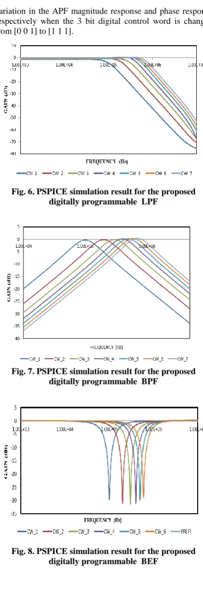
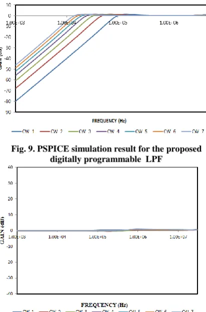
Fig. 6, Fig. 7,Fig. 8 and Fig. 9 show resultant waveforms for LPF, BPF, BEF and HPF respectively for different control words by changing the associated bits where each bit corresponds to a particular binary weight when varied from [0 0 1] to [1 1 1]. Fig. 10(a) and Fig 10(b) depicts the
[image:4.595.321.531.66.674.2]variation in the APF magnitude response and phase response respectively when the 3 bit digital control word is changed from [0 0 1] to [1 1 1].
Fig. 6. PSPICE simulation result for the proposed digitally programmable LPF
[image:4.595.53.271.76.221.2]Fig. 7. PSPICE simulation result for the proposed digitally programmable BPF
Fig. 8. PSPICE simulation result for the proposed digitally programmable BEF
Frequency
100Hz 300Hz 1.0KHz 3.0KHz 10KHz 30KHz 100KHz 300KHz 1.0MHz 3.0MHz 10MHz 1 DB(V(8)/V(1)) 2 P(V(8))
-30 -20 -10 0 10 G A I N
-80d -40d 0d 40d 80d P H A S E
>>
Frequency
1.0KHz 3.0KHz 10KHz 30KHz 100KHz 300KHz 1.0MHz
1 DB(V(6)/V(1)) 2 P(V(6)/V(1)) -100
-50 0 20 G A I N
0d 45d 90d 135d 180d P H A S E
>>
Frequency
1.0KHz 3.0KHz 10KHz 30KHz 100KHz 300KHz 1.0MHz 3.0MHz 1 DB(V(9)/V(1)) 2 P(V(9))
-40 -20 0 20 G A I N
-300d -200d -100d -0d
-360d P H A S E
[image:4.595.327.534.112.248.2] [image:4.595.54.275.301.437.2] [image:4.595.56.269.521.663.2]Fig. 9. PSPICE simulation result for the proposed digitally programmable LPF
Fig. 10(a): PSPICE simulation result for the proposed digitally programmable APF(Magnitude Response)
Fig. 10(b): PSPICE simulation result for the proposed digitally programmable APF(Phase Response)
[image:5.595.323.537.80.239.2]Furthermore, Fig. 11, Fig. 12 and Fig. 13 illustrate the variation in control frequency with different control words. All the plots are in excellent mathematical conformity with the transfer functions given in equations (6) through (10). The cut-off frequency is found to vary from 98.22KHz to 705.32 KHz for low-pass filter,98.52KHz to 716.122KHz for band-pass filter,14.12KHz to 98.16 KHz for high-band-pass filter, 99.526 KHz to 703.12 KHz forthe band-reject filter by changing the control word from [0 0 1] to [1 1 1]. All the proposed circuits are compatible with contemporary CMOS processes as only MOSFETs and grounded resistors and capacitors are employed to realize all the standard filter functions.
[image:5.595.319.538.83.407.2]Fig. 11: Variation of cut-off frequency of the proposed LPF with digital control word
Fig. 12: Variation of cut-off frequency of the proposed BPF with digital control word
Fig. 13: Variation of cut-off frequency of the proposed HPF with digital control word
6.
CONCLUSION
[image:5.595.60.271.430.564.2] [image:5.595.325.540.460.601.2]7.
REFERENCES
[1] B. Wilson.Recent developments in current conveyor and current-mode circuits. IEEE Proceedings-Circuits Devicesand Systems,137: 63–77, 1990.
[2] J. W. Horng, W. Y. Chiu, and H. Y. Wei. Voltage-mode high-pass, band-pass and low-pass filters using two DDCCs. Int. J. Electron., 91: 461–464, 2004.
[3] J. W. Horng and M. H. Lee. High input impedance voltage-mode low-pass, band-pass and high-pass filter using current-feedback amplifiers. Electronic. Letters, 33:.947–948, 1997.
[4] S. Maheshwari, J. Mohan, and D.S. Chauhan. Novel cascadable all-pass/notch filters using a single FDCCII and grounded capacitors. Circuits, Systems, and Signal Processing,30:643–654,2011
[5] S. Minaei and E. Yuce. Novel voltage-mode all-pass filter based on using DVCCS. Circuits, Systems, and Signal Processing, 29:391–402, 2010.
[6] M.Z. Khan and M.S. Ansari. DVCC-based Electronically Tunable First-Order Current-mode Filters. International Journal of Computer Applications, 48(15):21-24, 2012.
[7] A.A. El-Adawy, A.M. Soliman, and H.O. Elwan. A novel fully differential current conveyor and applications for analog VLSI. IEEE Transactions-Circuits and Systems II: Analog and Digital Signal Processing 47(4):306 –313, 2000.
[8] C. Cakir, U. Cam, and O. Cicekoglu. Novel all-passfilt- -erconfiguration employing single OTRA. IEEE
Transactions-Circuits and Systems II: Express Briefs, 52(3):122 – 125, 2005
[9] H.O. Elwan and A.M. Soliman. Novel CMOS differential voltage current conveyor and its applications. IEE Proceedings - Circuits, Devices and Systems, 144(3):195–200, Jun 1997.
[10] S. Minaei and M.A. Ibrahim, General configuration for realizing current-mode first-order all-pass filter using DVCC. International Journal of Electronics, 92(6):347– 356, 2005.
[11] U. Cam. A new trans-admittance type first-order all-pass filter employing single third generation current conveyor. Analog Integrated Circuits and Signal Processing, 43:97– 99, 2005.
[12] S. Minaei and M.A. Ibrahim. A mixedmode KHN -biquad using DVCC and grounded passive elements suitable for direct cascading. International Journal of Circuit Theory and Applications, 37(7):793–810, 2009.
[13] W.Y. Chiu, J.W. Horng, H. Lee and C.C Huang, "DVCC-Based Voltage-Mode Biquadratic Filter with High-Input Impedance," pp.121-125, Fifth IEEE International Symposium on Electronic Design, Test & Applications, 2010.
![Fig. 3. CMOS realization of Digitally Controlled DVCC with gain k[14]](https://thumb-us.123doks.com/thumbv2/123dok_us/8102837.788427/2.595.93.253.234.353/fig-cmos-realization-digitally-controlled-dvcc-gain-k.webp)