Different Parameter Analysis of CMOS Charge Sharing
Latch Comparator using 90nm Technology
Ajay Vishwakarma
School of Electronics Engineering, VLSI Division,VITUniversity, India
Sweta Sahu
School of Electronics Engineering, VLSI Division,VITUniversity, India
Richa Soni
School of Electronics Engineering, VLSI Division,VITUniversity, India
Vijay Vishwakarma
School of Electronics Engineering, VLSI Division,VITUniversity, India
ABSTRACT
In the present works, mainly power consumption of circuit is main issue for every designers. This paper mainly dealing with the implementation of CMOS Charge sharing latch Comparator and analysis of it using different parameter in 90nm.For the implementation of new design the features of two important Comparator are combined so that the power dissipation is reduced and speed of new design is increased. These two Comparator are Resistive Dividing Comparator and Differential Current sensing respectively. The simulation result is shown in 90nm technologies, for 2.4GHz clocked comparator by using 0.9V input. Again the result of 90nm technology is compared with 180nm technology to show the reduction of power and enhancement of speed. The implementation is done on the Cadence virtuoso design environment.
Keyword: Power analysis, CMOS latch comparators.
1.
INTRODUCTION
Now a days, its requires the use of very low devices in the circuits and systems. Low power A/D converters ,sense amplifier and data converter, which is used for many application is using comparator as its basic element which causes reduction in power consumption by removing pre-amplifying stage. Due to removal of many pre amplifier stages area also get reduced. Voltage Comparator are generally used as a first stage of ADC design and output of the Comparator is used as time reference to mark the input value threshold crossing of the circuit.
In comparator design it uses back to back inverter and positive feedback mechanism for the convertion of small input voltage to full scale digital value. For such type of comparator offset voltages due to device mismatch like threshold voltages, current factor, internal/external capacitance is main limitation. To eliminate this limitation comparator uses pre-amplifier stages before latch so that correct output can be produced. But pre–amplifier stages also has some disadvantages that it
consume more static power and reduced gain due to varying technology scale, and latch comparator without pre-amplifier stage is desirable with using digital calibration technique. Comparator is a circuit which compares the Analog signal with reference signal and produces Digital full scale output according to the comparisons
Above diagram shows the basic operation of Comparator circuit.
In this paper it is discussed charge sharing latch comparator which shows power improvement compare to comparator using pre-amplifier stages. Here two main comparators are discussed below which good features are combined and used for new charge sharing topology. Let starts our discussion form two basic circuits, before discussing new design [1][2][3][4].
1.
1 Resistive Dividing Comparator
This is the basic circuit of Comparator which is used for the new design implementation. This circuit is simple and more easily can be analysed. Here the main problem is more power consumption for the resistive dividing circuit in reset mode which causes power dissipation.[5],[6].
The circuit operation is given below and fig.1 shown for the resistive dividing Comparator.
Reset phase:
When the clk is low circuit comes to reset phase. Here the M11 get turn off, and circuit is cut off from the ground. Precharging of circuit starts working as transistor M1 and M2 get turn-on which causes the output to charge to Vdd. And Vdd charges both the output capacitor which result in power consumption.
Regeneration phase:
When clk is high it started to come in regeneration phase, and M11 get turn on.M1 and M2 turns off. So now the circuit starts comparing the two input voltages.
[image:2.595.334.513.75.271.2]Advantages of this comparator are it is easy to adjust the threshold voltage by varying the transistor width instead of changing any of reference voltages.
Fig.1: Resistive Dividing Comparator
1
.2 Differential Current Sensing comparator:
The main advantage of this comparator is that its comparing circuit convert the input voltages to differential current at the output. Mainly it uses M12 transistor which connect both output together to share the charges instead of pre-charging to Vdd. Given below is the circuit diagram in fig.2.
During Reset phase output charge will drained off through transistor M4-M5. Now during regeneration phase when clk is low then M12 get turn off and M1 is on. This starts latch circuit to work in regeneration mode. When the output is higher than threshold voltage M6 and M7 gets turn on and its connected the output to the input comparing circuit. At the end output with low conductance change to Vdd and high conductance is change to ground.[6],[7].
[image:2.595.83.245.265.449.2]A disadvantage of circuit is that it consumes more power to drive current at regeneration phase by both output.
Fig.2: Differential Current Sensing Comparator
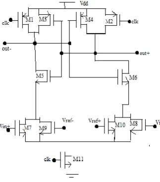
1.3 Implemented new design of Comparator
This is the new implemented design circuit which is used for the consideration and its simulation result is performed and analysed and compared in both technology 180nm and 90nm. The good properties of above two comparators are used in this design which is pass transistor which share the charges and width is variable to reduce threshold voltages. This greatly reduces the power consumption both at reset and regeneration phase by cut-off of pre-charging circuit and sharing charges at both load capacitors which makes output not to go below threshold voltage so that input can be compare faster during regeneration interval.
The operation of the circuit is as follows.
Fig.3: Charge sharing latch comparator
2.
SIMULATION RESULTS
Design has been simulated in both 180nm and 90nm process technologies and the results are compared with those in old paper[6]. Lower power consumption and high operational speed is most useful part of this design.
[image:3.595.318.529.71.248.2]2.1
180nm technology
Table.1 CMOS technology parameter
All Pmos All Nmos
Width 6000nm 3000nm
Length 180nm 180nm
2.1.1
Dc analysis: Gain: 25.61dB
Fig.4: Dc waveform between input and output voltages
2.1.2
Transient analysis
Fig.5: Transient waveform
2.1.3 Analysis of Noise Signal:
Output Noise value: 9.97µV/sq(Hz)Fig.6: Output Noise Waveform
[image:3.595.51.275.417.692.2]2.2
90nm technology:
Table.2 CMOS technology parameter
All PMOS All NMOS
Width 240 nm 120nm
Lenght 100nm 100nm
2.2.1 Output voltage
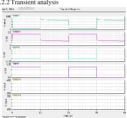
[image:3.595.311.543.440.709.2]2.2.2
Transient analysis
Fig.8: Transient waveform of charge sharing comparator
3.
ANALYSIS USING DIFFERENT
PARAMETERS
3.1
Technology Effect:
In these paper 90nm technology is used which having channel length smaller than the 180nm technology. This improves speed of the design.
3.2 Transistor width Effect:
For this paper it is used 6000nm width Pmos and 3000nm width Nmos in 180nm technology and 240nm for Pmos and 120nm width for Nmos in 90nm technology. So the new design showed speed decrement compared to 180nm, but the area of the design is smaller. From the below waveforms it is shown that as width increases the delay of the circuit decreases. As width increases from 6µm to 10µm delay line increases from line 1 to 5 shown below in fig.9.Same result also is for fig.10.
[image:4.595.318.534.76.228.2]180nm technology
Fig.9: Simulation result for Different value of width in 180nm
90nm technology
Fig.10: Simulation result for Different value of width in 90nm
From above discussion it is concluded that as width increases, speed get increased because propagation delay increases as capacitor takes more time to charge and discharge, but area improves.
3.3 Load capacitance Effect:
Capacitor mostly used to reduce any ripples coming in the power supply voltages [8],[9]. Basically it is used for elimination of offset voltages, so capacitor value should provide low to reduce the error in the output voltages. Smaller is the Capacitor, faster is the output value. Capacitor equation is shown below:
T=RC Equation (1)
From the fig.11 is shown that the C=0.1pF increases to 2pF then delay also increases from 1 to 4 lines and design becoming slower. Same result for fig.12.
[image:4.595.318.539.471.578.2]180nm technology
Fig.11: Simulation result for Different value of load verses Vin in 180nm
[image:4.595.62.269.557.724.2]90nm technology
[image:4.595.317.539.583.748.2]In this paper load capacitance 100fF is used for 180nm and 4fF is used for 90nm which is connected at the Vout+ and Vout-, it concluded that more capacitor causes more delay.
4
ANALYSIS OF DELAY
Propagation delay is the time taking by the input to change to produce corresponding change in the output signal. Design is faster as the delay reduces, in the circuit.
Below are given the transient response of the design in both 180nm and 90nm technology.[10]
180nm technology
Fig.13: Propagation delay of the 180nm
[image:5.595.312.546.76.219.2]90nm technology
[image:5.595.59.269.221.559.2]Fig.14: Propagation delay of the 90nm
Table.3 COMPARISONS OF THE PROPAGATION DELAYS
Tplh Tphl
180nm Vout+
Vout-
3.8ns
0.46ns
0.51ns
2.72ns
90nm Vout+
Vout-
0.03ns
0.01ns
0.04ns
0.04ns
So form the above Table.3 it is shown that for both the output delay is less in 90nm compares to 180nm technology.
5
POWER ANALYSIS
Power dissipation is the rate at which energy is dissipated from electrical circuits. It is measured in watts.
P=Idd.vdd Equation (2)
For the comparator design power dissipation increases as area increases due to leakage form circuits, so in 90nm it is concluded from above discussion that area is smaller than the 180nm so power dissipation is reduced in 90nm process technology and it get more power saving design.
6
RESULT TABLE
Table.4 Comparison Result of Comparator Design
180nm design Present Design(90nm)
length 180nm 90nm
Load capacitance
100fF 4fF
Clock frequency
50Mhz 50Mhz
Wp/Wn 6µm/3µm 0.24 µm/0.12 µm
Voltage Supply 1.8V 1V
Delay 1.59ns 0.035ns
Static power dissipation
41.7pW 20.34pW
Average power dissipation
173.15µW 69.81 µW
Equivalent output noise
[image:5.595.311.549.431.737.2]
7
LAYOUT
Layout of presently designed Comparator is shown below in 180nm process technology and its DRC and LVS report is also checked.
8.
CONCLUSION
In this paper the CMOS Charge Sharing Latch Comparator is implemented in both 90nm and 180nm technology. Its simulation results and various parameters is compared for both technology. Here the input voltages used are 0.9V and 1.8V.The implemented new design shows reduction of power and enhancement of speed in lower technology than 180nm, comparision result is shown in Table.3.
From the result, it is found that the average power dissipation is reduced approximately 61% in 90nm compared to the 180nm and the delay minimizes to 0.035ns. Hence it is concluded that in 90nm Comparator operate with higher speed and provide more stabilized Output compare to 180nm.
9. REFERENCES
[1] R. Wang, Kaihang Li, J. Zhang, Bin Nie, “ A High Speed High Resolution Latch Comparator for pipeline ADC”, pp 28-31, IEEE, 2007.
[2] S .Sheikaei, S.Mirabbasi, and A. Ivanov, “A 0.35µm CMOS Comparator Circuit For High-Speed ADC Applications”, pp 6134-6137, IEEE, 2007.
[3] Khosrov Dabbagh Sadeghipour,” Resolution Enhanced latch Comparator”, pp 29-35, IEEE ,2001. [4] Meghana Kulkarni, V.Sridhar , G.H.Kulkarni,”The
Quantized Differential Comparator in Flash Analog to Digital C design” Vol.2, No.4, july 2010, IJCNC. [5] Hao Gao, Peter Baltus and Qiao Meng,” Low voltage
comparator for High Speed ADC”, ISSSE 2010. [6] P.Uthaichana and E.Leelarasmee, “Low power CMOS Dynamic Latch Comparators,”IEEE, pp.605-608, 2003.
[7] Z .Huang and P. Zhong,” An Adaptive Analog –to-Digital Converter Based on Low-Power Dynamic latchcomparator,” IEEE Conference , p.6pp, 2005. [8] Soheli Farhan, A.H.M. Zahirul Alam, Sheroz Khan, Md.
Ataur Rahman,” Design of a Comparator for Quaternary Multi Valued Analog to Digital Converter,” IEEE 2011.
[9] HeungJun Jeon, Yong-Bin Kim and Minsu Choi,”Offset Voltage Analysis of Dynamic Latched Comparator”,IEEE, 2011.
[10] B. T. Turko and W.F. Kolbe ,”Ultra- Fast Voltage Comparators For Transient Waveform Analysis”, Vol.37, No.2, IEEE Transaction On Nuclear Science, April 1990.
[11] P. R. Gray and R. G. Meyer, “Analysis and Design of analog Integrated Circuits”. John Wiley & Sons,Inc.,third edition ed., 1993.
[12] R.J.Baker, E.Institute of, E.Electronics, and I.S.-S. C. Society, CMOS: circuit design, layout, and simulation: IEEE Press, 2008.
[13] A.P.Godse and D.A. Godse, Digital system Design-I:Technical publications 2008.