NEW SOLAR-CELL COATING TO ENABLE BOOST IN
EFFICIENCY
1J.MANJU,2 DR.S.JOSEPHJAWHAR,
1 Research Scholar,Sivaji College of Engineering and Technology, Manivila.
KanyakumariDistrict,Tamilnadu, India.
2 Principal, Arunachala College of Engineering for Women,
Vellichanthai,KanyakumariDistrict,Tamilnadu,India.
E-mail: [email protected], [email protected]
ABSTRACT
These days Solar Energy is discriminatingly required to satisfy the human needs. Anyway amid the energy conversion [sunlight into Current] the measure of transformation is not sufficient and it is less because of sun powered shaft reflection on the surface of the solar panel.This strategy never surpasses 34% for a solitary advanced semiconductor intersection. The current framework utilized aqueous strategy, and
the nanoparticles arranged are co-doped and the immaculate and the
transformation proficiency arrive at up to 9.07%. The main objective of this paper is to improve the energy conversion rate in terms of reducing the Reflection. In the past studies in photovoltaic [PV] cell, if one proton thumps then one electron detached in the PV material. In this paper another system is presented where in a PV cell, every photon can rather thump two electrons detached by changing the semiconductor as ′ ′ and which gets to be components. This makes the process significantly more productive than the current methodologies. In a standard cell, any overabundance energy conveyed by a photon is squandered as high temperature, although in the new framework the additional energy goes into handling two electrons rather than one. The resultant current is very nearly straightforwardly corresponding to the force of the light.
Keywords:Solar Cell; Photovoltaic; Energy Efficiency; Photon; Electron.
.
1. NOMENCLATURE
Symbols Description
ARC Anti-Reflection Coating
PV Photovoltaic
Si Silicon
PO Phosphorous
TiOx Titanium Oxide
SIMS Secondary Ion Mass Spectroscopy
PO Phosphorous
SiNx Silicon Nitride
CeO2 Cerium Oxide
c-Si Cesium Iodide
Al2O3 Aluminum Oxide
PSG Phosphors-Silicate Glass
eV Electron Energy
NTPV Near Field Thermophotovoltaic
2. INTRODUCTION
any ARC material. The principle target of ARC is to ingest however much as could be expected daylight which falls on the highest point of the sun based cells. The surface of the silicon substrate could be secured with single or twofold against reflective coatings to enhance the benefit of energy suing sun based cells.
ARC could be gotten by Doping applicable materials on the silicon. Doping might be utilized to change the amount of electrons and openings alertly in semiconductors. Doping
makes [majority carriers are
negative] material semiconductor from group-IV into group-V atoms. N-type materials build the conductivity of a semiconductor by expanding the amount of accessible electrons. P-sort materials build conductivity by expanding the amount of openings present.
In this paper binding silicon hole with group-V elements electrons makes a new bond. Group-V elements’ atoms are having one or more valence electron more than silicon which is
going to use are converted into ‘ ’
semiconductor material. Since group-V
elements’ atoms are having 5 valence electrons that can create covalent bonds with the 4 valence electrons in available in the silicon atoms. For the reason in each atom the 4 valence electrons needs to form covalent bonds around the silicon atoms. The additional valence electron [n-type material have 5 valence electrons] present when the two atoms bond is free to participate in conduction. Consequently extra electrons are added to the conduction band and for this reason it increases the number of electrons present now.
3. RELATED WORKS
In this paper author have done the similar
reproductions investigation of N-type ! "#
Solar Cell with "#$%&'"#$% ()2 layers
independently by PC1D reproduction
programming. The inspiration of this paper is to focus the ideal condition when Solar Cell yields more productivity by utilizing SiNx +CeO2 layer
as opposed to just "#$% layer individually on the
front side of the Solar Cell [1]. An outline of
new innovation kept to ('"&'+#)2 is
displayed and the properties, the points of interest of the mixture sunlight based cell
utilizing ('"&'+#)2 have been examined in
subtle element [2]. One of the earlier papers had concentrated on the advancement of a basic and minimal effort option to these saved coatings
(ARC), through the utilization of an
electrochemical carving procedure to structure AR layers of silicon (mc-Si). [3]. Another paper
report a novel reviewed refractive list
antireflection covering for III/V fourfold sun based cells focused around bottom up become decreased GaPnano wires.[4].
In occurrence of resonant surface modes such as surface polaritons, the instability substituted in near field between source and photodiode radically disables the propagative support [5-9]. This innovation has released new opportunities for the progress of state-of-the-art technologies for nano-scale thermal organization, heating-assisted data storage [10], IR detecting and spectroscopy [11, 12] and has covered the way to a novel generation of NTPV energy-conversion strategies [13, 14]. In the situation of heat transmission, the part of graphene has been
newly examined [15-18], confirming its
tunability and paving the way to encouraging thermal devices such as thermal transistors. Also, a NTPV cell in which a deferred graphene sheet performance as source has been newly considered [19].
A bilayer covering of ,-2)3 &'+#)2 is
of splash on sunlight based cells[24]. One of the earlier work, the author looked at the properties of multi crystalline silicon sunlight based cells which relied on upon the sort of emulating
antireflective layers: & "#: (: 2, &
"#: $: 2&'+#)%[25].
4. PROBLEM STATEMENT
Current energy conversion through 45 -#67 is a standout amongst the most in-exorbitant ways utilizing common data. Anyway basically sun oriented cells cannot change over all the light fall on its surface into energy. 40% to 60% of the daylight is pondered while fall on the surface. It is important to keep away from this light reflection by giving a right ARC on the surface of the sun powered board. In this paper changing the immaculateness of the silicon by doping phosphorous on the highest point of the silicon-cell the measure of light perception might be expanded.
4.1. Silicon Vs. Solar Cell
One of the fundamental compound properties is the crystalline manifestation of the silicon. In silicon one molecule has fourteen electrons set in three separate shells. The main shell hold two electrons and the second shell hold eight electrons [completely full]. The third shell has just four electrons [half full]. The conduct of the silicon is, it generally attempt to fill the third cell dependably. For this it conveys its electrons with the nearby by iotas. Every particle has four hands and it joins with four neighbors and makes the crystalline structure which brings a paramount to this kind of PVS cell.
Figure-1: Structure Of Silicon Crystalline
Unadulterated crystalline silicon is a poor conductor so that the silicon accessible in sun oriented cells has debasements. To ruin the sunlight based virtue different iotas are blended
intentionally in with the silicon particles which change the conduct of the work a bit. We
basically consider polluting influences
something undesirable, yet in this paper the
silicon cell wouldn't work without
contaminations. To make the debasements the phosphorous is included due to phosphorous has five electrons in its external shell [not other numbers] which might be gone to the Silicon. Potential outcomes are there to adjust the amount of electrons with openings by moving in a silicon gem cross section by doping with alternate iotas.
5. PHOTOVOLTAIC CELLS:
CONVERTING PHOTONS TO ELECTRONS
The sun based cells accessible on the mini-computer and satellites are named as PV cells which changes over the light into energy.
8 9 :8
∶ <:9 9 :;
One sun oriented board is a gathering of cells joined electrically and stuffed into a plastic or glass outline. PV cells are produced by semiconductors, for example, silicon, which is
presently utilized generally ordinarily.
Fundamentally, when light strikes the cell, a certain bit of it is assimilated inside the semiconductor material. This implies that the energy of the assimilated light is exchanged to the semiconductor. The energy thumps electrons
detached, permitting them to stream
unreservedly.
PV cells additionally all have one or more electric field those demonstrations to compel electrons liberated by light retention to stream in a certain heading. This stream of electrons is a current, and by setting metal contacts on the top and lowest part of the PV cell, we can draw that present off for outer use, say, to power a mini-computer. This present, together with the cell's voltage (which is an aftereffect of its inherent electric field or fields), characterizes the force (or wattage) that the sun oriented cell can prepare.
That is the essential procedure, however there's truly a great deal more to it. On the following page, how about we investigate one sample of a PV cell: the single-gem silicon cell.
5.1. Proposed Doping Method
In as a relatable point semiconductor
there may be 10!@ dominant part bearers
AB& CDB5 E
F %&@-: /7B47BDB54G
HB'4 I%!44 I-!DB4
J&KBD#(&DD#D4 I-!DB4
J#BD#(&DD#D4 2B-4
Table-1: Periodic Table
In this paper the doping of phosphorous is possible by tube heater under low weight
atmosphere F200@L&DG. To place high number
of wafers into the quartz, it is set vertically and it
can underpins for setting 156 % 156 @@ .
Among the wafers a balance quality is kept up [3 mm] and heat conversion is connected at the
most extreme level of 890°!. Since the
phosphorous is as fluid, it will be conveyed by the stream of Nitrogen through air pocket trap. Before doping phosphorous, oxygen is infused to assurance the warm erosion of silicon. The doping of phosphorous from the surface happens
upon diminishment of /) by silicon as per:
S T:U VWTU → VW TU YSTU.
Throughout the time of high temperature warming phosphorous is doped into silicon lattice structuring the p-n intersection. In the wake of doping the thickness of the wafers is
getting expanded. While doping /"C is
structured on the surface of the silicon cells and it is the blending of phosphorous pentoxide and silicon dioxide. /"C is engraved by fluorydric corrosive 10% for the span of 5 prior minutes SIMS and sheet safety characterization.
Extraneous semiconductors are structured by including particular measures of contamination particles to the silicon gem. A n-sort semiconductor is structured by doping the silicon precious stone with components of Group-V demonstrated in Table-1. In a semiconductor material the law of mass action states that
Z 9 I[5 F1G
\7D
8 8: 9
8 : 9.
]BD #D#4#! 4@#!B'5!BD
, Z Z -- Equ [2]
AndEqu [1] becomes
Z
In this paper a scientific model of phosphorous doping profile is utilized for recreation. It will be watched that a typical PV cell can produce a voltage around 0.5 to 0.8 volts depending on the sort of semiconductor and the manufactured up innovation. Under top daylight conditions a regular business PV cell with a surface zone of about 25 square crawls will handle something like 2 watts crest power. Since a single cell can prepare just a exceptionally law current and voltage, cells joined in arrangement can get a high voltage while keeping the same current.
6. RESULTS AND DISCUSSION
An example PV module is produced number of cells joined in parallel, number of cells associated in arrangement and the voltage, current strength is dissected and the result is given underneath. As indicated by the lambda esteem the current generation is getting changed
relatively for a steady voltage. The
qualities are executed in the matlab and the recreation come about that is exhibited underneath.
Figure-2:Vpv - Ipv Model For Different
Irradiation For A Constant Temperature.
As shown in Fig.2 "B-&D 36^ /E
module characteristics depend on the Irradiance
when the temp is at 25(. When the Irradiance
increases from 200^/"[@ to 1000^/"[@ the
output current also increases.
6.1 Diffusion Capacitance
When a junction is forward biased,
holes are injected from the 4#' of the
metallurgical junction into the
material. The holes are momentarily stored in the
material before they injected into
temporarily stored in the material. The
electrons then recombine with the majority
carriers (holes) in the @&D#&-. The
minority carriers charge around the metallurgical junction as the result of forward biasing the pn junction. Changing the forward current of
forward voltage, ∆E, will result in the change in
the value of the stored charge , ∆`, the diffusion
capacitance, (' can be found from the general
formula
( Z∆
∆, It turns out that the diffusion
capacitance is proportional to forward-biased
current. That is( Z ab , wherea is
constant at a given temperature, bis forward-
biased diode current.
Figure-3: Diffusion And Depletion Capacitance
Shows the depletion and diffusion capacitanc
e of a forward- biased junction :
b Z bTೇೞೖ 1U
(Z ab
6.2.Mobile Carriers
Silicon is the most commonly used semiconductor material in the integrated circuit industry. Silicon has four valence electrons and its atoms are bound together by covalent bonds. At absolute zero temperature the valence band is completely filled with electrons and no current flow can take place. As the temperature of a silicon crystal is raised, there is increased probability of breaking covalent bonds and freeing electrons. The vacancies left by the freed electrons as holes. The process of creating free electron-hole pairs is called ionization. The free electrons move in the conduction band. The average number of carriers (mobile electrons or holes) that exist in an intrinsic semiconductor material may be found from the mass-action law:
Silicon is the most normally utilized semiconductor material within the incorporated circuit industry. Silicon has four valence electrons and its iotas are bound together by covalent bonds. At outright zero temperature the valence band is totally loaded with electrons and
no present stream can occur. As the temperature of a silicon precious stone is raised, there is expanded likelihood of breaking covalent bonds and liberating electrons. The opening left by the liberated electrons makes the openings. The procedure of making free electron-gap sets is called ionization. The free electrons move in the conduction band. The normal number of transporters (portable electrons or openings) that exist in an inherent semiconductor material may be found from the mass-movement law:
Z ,+./
Where
+is the absolute temperature in °K
ais Boltzmann’s constant Tc Z 1.38 d
10
U.
Figure-4: Electron Concentration Vs. Temperature
6.3.Current Density And Mobility
Two mechanisms account for the movement of carriers in a semiconductor material: drift and diffusion. Drift current is caused by the application of an electric field, whereas diffusion current is obtained when is a net flow of carriers from a region of high concentration to a region of low concentration. The total drift current drift density in an extrinsic semiconductor material is
e Z [T ∝ ∝ UI
J is current density N is
mobile electrons density P is hole density
∝ #4 @BL#-# Bg & 7B- Q is the electron charge
E is electric field
From measured data, an empirical relationshi
p between electron (µn) and hole (µp) mobility’s
vs doping concentration at 300°,
∝T$U Z5.1%10
! 92$
".#
3.75%10 $".#
∝ T$$U Z2.0%10 47.7$$". 5.86%10 $$".
Where $ and $$ are donor and acceptor
[image:6.595.83.521.72.798.2]concentration per !@, respectively.
Figure-5:
Shows The Plot Of Mobilityversus Doping Concentrati on
For an semiconductor at
300° a, if the doping concentration is varied
from 1013 B 1018 &B@4/! @, determine the
minority carriers in the doped shows the hole concentration versus doped semiconductor shows the hole concentration versus doping.
≅ $
≅
$
In a semiconductor, the
acceptor concentration $$ is greater than the
intrinsic hole concentration Z .
From the above equation we can get,
Electron concentration= $ and
Hole concentration = మ
%ವ
Where
Z 1.52 d 10" -!DB4/!@
Figure 6: Hole Concentration In N-Type Semiconductor (Si).
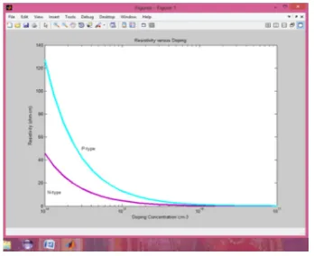
At the temperature of 300°a, the resistivity of sil
icon doped by phosphorus is given as,
kZ 3.75%10
$
".#
1.47%10$.# 8.15%10$
A similar relation for silicon doped with boron is given as,
k Z 5.86%10
$
$".
7.63%10!$$. 4.64 ∗ 10&$$
Where, $ and $$ are donor and acceptor
concentrations, respectively.
Figure 7: Resistivity Versus Doping Concentration
Since the resistivity of N-type is very less the energy generation is high in the solar cell by doping Group-V element as Phosphorous.
Variou s Size
Existing System ሾࢋࢂሿ
Proposed System ሾࢋࢂሿ
% of
Improvement ሾࢋࢂሿ
2’ x 4’ 1.2 1.4 .2
3’ x 6’ 3.7 4.3 .6
[image:6.595.326.500.460.602.2]3’ x 10’
12.23 32.16 19.93
Table-2: Existing Vs. Proposed Comparison In Terms
Of ܸ݁
The above table shows the comparative
results of E generation before and after doping
phosphorus on the solar panel. This experiment is handled in real time for various size of solar panel and the improved percentage of energy obtained is given.
7. CONCLUSION
Solar energy conversion is most important and this paper provides a very good solution to improve the energy efficiency. This paper concentrates on the doping of phosphorus to improve the n-type model.
The technique used is to create a Group-V component which most efficient way to doping Nano particle in a stipulated time.
A built Group-V component based doping was performed to demonstrate that the exploratory doping time, temperature; n-sort vs. p-sort material can control the intersection profundity and also the framed emitter quality. The phosphorous doping procedure streamlining and association among doping profile and the sun based cell execution is contemplated
hypothetically and code mimicked in
Matlab2012a programming. The sun powered cell productivity could be enhanced by changing over the semiconductor as n-sort model. The similar results are indicated in the recreation figures.
8. LIMITATIONS
The energy conversion rate can be improved according to the Anti-Reflection-Coating Material. It can be improved by mixing various materials [Nano-Particles] and test the energy conversion rate.
REFERENCES
[1]. U. Gangopadhyay, S. Ray, E. Panda, S. Jana, S. Das, “Efficiency enhancement of Solar Cell by introduction of Cerium Oxide along with Silicon Nitride”, International Journal of Renewable and Sustainable Energy 2013; 2(2) : 46-50
[2]. Dr. MrunalDeshpande*, Dr.R.Seyezhai**, “REVIEW OF HYBRID SOLAR CELLS
BASED ON CdSe AND TiO2
MATERIALS”, International Journal of
Innovative Research in Computer and Communication Engineering, Vol. 2, Issue 3, March 2014
[3]. A. Ibrahim, A.A. El-Amin, “Etching, Evaporated Contacts and Antireflection Coating on Multicrystalline Silicon Solar Cell”, INTERNATIONAL JOURNAL of RENEWABLE ENERGY RESEARCH A., Vol.2, No.3, 2012.
[4].Silke L. Diedenhofen, GrzegorzGrzela, Erik
Haverkamp, GerardBauhuis, John
Schermer, Jaime G´omez Rivas,
“Broadband and Omnidirectional Anti-reflection Layer for III/V Multi-junctio Solar Cells”, October 25, 2012.
[5]. A. Kittel et al., Phys. Rev. Lett. 95, 224301 (2005).
[6]. L. Hu et al., Appl. Phys. Lett. 92, 133106 (2008).
[7]. S. Shen, A. Narayanaswamy, and G. Chen, Nano Letters 9, 2909 (2009).
[8]. T. Kralik et al., Rev. Sci. Instrum. 82, 055106 (2011).
[9]. R. S. Ottens et al., Phys. Rev. Lett. 107, 014301 (2011).
[10]. W. Srituravanich et al., Nano Lett. 4, 1085 (2004).
[11]. Y. De Wilde et al., Nature 444, 740 (2006).
[12]. A. C. Jones and M. B. Raschke, Nano Letters 12, 1475 (2012).
[13]. A. Narayanaswamy and G. Chen, Appl. Phys. Lett. 82, 3544 (2003).
[14]. M. Laroche, R. Carminati, and J. J. Gre_et, J. Appl. Phys. 100, 063704 (2006).
[15]. B. N. J. Persson and H. Ueba, J. Phys. Condens. Matter 22, 462201 (2010). [16] A.I. Volokitin and B. N. J. Persson, Phys.
Rev. B 83, 241407(R) (2011).
[17]. V. B. Svetovoy, P. J. van Zwol, and J. Chevrier, Phys. Rev. B 85, 155418 (2012). [18]. O. Ilic, M. Jablan, J. D. Joannopoulos, I.
Celanovic, H. Buljan, and M. Solja_ci_c, Phys. Rev. B 85, 155422 (2012).
[19]. O. Ilic, M. Jablan, J. D. Joannopoulos, I. Celanovic, H. Buljan, and M. Solja_ci_c, Opt. Express 20, A366 (2012).
[20].Benjamin G Lee, JarmoSkarp, Ville Malinen, Shuo Li, Sukgeun Choi, Howard M. Branz, “Excellent Passivation and Low Reflectivity Al2O3/TiO2 Bilayer Coatings for n-Wafer Silicon Solar Cells”, June 2012.
Cell Efficiency”, Int. J. Electrochem. Sci., 7 (2012) 376 – 386.
[22]. Chien-Ming Lee, Sheng-Po Chang, Shoou-Jinn Chang, Ching-In Wu, “Fabrication of High-Efficiency Silicon Solar Cells by Ion Implant Process”, Int. J. Electrochem. Sci., 8 (2013) 7634 – 7645.
[23]. SayedaAnika Amin, SartazTabinnaSalim, and K.M.A. Salam, “Cadmium Selenide and Cadmium Telluride Based High Efficiency MultijunctionPhotovoltaics for Solar Energy Harvesting”, International Journal of Electrical Energy, Vol.1, No.1, March 2013.
[24]. MortezaEslamian, “Spray-on Thin Film PV Solar Cells: Advances, Potentials and Challenges”, Coatings 2014.
[25]. BARBARA SWATOWSKA1, TOMASZ
STAPINSKI1, KAZIMIERZ