handbook
1973-74
prepared
by
Copyright
©
1973 by Digital Equipment CorporationDigital Equipment Corporation makes no representa-tion that the interconnecrepresenta-tion of its modular. circuits in the manner described herein will not infringe on existing or future patent rights. Nor do the descrip-tions contained herein imply the granting of licenses to make, use, or sell equipment constructed in accord-ance herewith.
Digital Equipment Corporation is not responsible for errors which may appear in the pricing, technical descriptions, illustrations, or photographs of the products appearing in this, Handbook.
Digital Equipment Corporation reserves the· right to make substitutions and modifications in the specifica-tions of the products described in 'this Handbook. Prices quoted are in
u.s.
dollars and apply to the United States only. The availability of products listed and the prices quoted herein are subject to change without notice.FLIP CHIP, UNIBUS and OMNIBUS are trademarks of Digital Equipment Corporation,
Maynard, Massachusetts.
PRODUCT INDEX ...
v
FOREWORD... xix
INTRODUCTION ... xxi
Organization of Handbook ... xxi
M Series Module Selector Guide ... xxiii
Digital Equipment Corporation Engineering Services ... ... xxiii
Special Symbols and Abbreviations ... xxiii
Module Dimensions ... xxviii
M SERIES LOGIC AND CONTROL MODULES ... ... 1
List of Modules ... ... ... ... ... 3
General Characteristics ... ... ... 5
Module Descriptions ... ... ... 21
M SERIES MODULES FOR COMPUTER INTERFACING ... ... 145
OMNIBUS and UNIBUS Interface Modules ... 147
OMNIBUS/UNIBUS Electrical Characteristics ... 148
External I/O Bus (Positive Logic) ... : ... 152
Negative Bus ... 154
PDP-15 Bus ... 154
Module Description ... : ... 155
RTM MODU LES ... 263
A SERIES ANALOG MODULES ... ... ... ... ... ... 267
Notes on Operational Amplifiers ... ... ... ... 269
2" and Resolution ... 276
Digital Codes for A/ D's, D/ A's, and Data Acquisition Systems ... 277
Module Descript[ons ... '" ... 278
ACCESSORY MODULES ... 339
Wire Wrappable Module Boards ... 341
Collage Mounting Boards... ... ... ... ... ... ... ... .... 347
Blank Modules ... 348
Module Extenders ... 352
Bus Connectors ... ... ... .... ... ... 356
DEC KITS ... 359
DECkit11-H Input/Output Kit ... 362
DECkit11-F Input/Output Kit ... 364
DECkit11-K Input/Output Kit ... 365
POWER SUPPLIES Power Supplies and Accessories Summary ... ... .... ... ... ... ... 369
Power Supply Descriptions .. ... ... ... ..•. ... ... ... ... 374
CABLES AND ACCESSORIES ... 393
Standard Cables... .... ... .... ... .... ... ... ... .... ... ... ... ... 395
Cable Connectors ... '405
I/O Connectors ... 426
HARDWARE ... 429
Connector Blocks ... 432
Mounting Panels ... 439
Module Drawers ... 450
Mounting Panel Frames ... 453
Cabinets ... 455
Wire Wrapping Service ... 471
Accessories ... ... ... 475
DATA ENTRY TERMINALS ... 485
RTOI and RT02 ... ; ...• 486
LAB SERIES ... 491
. Computer Lab ... 492
K Series Logic Lab ... ... ... 495
M Series Lab ... 503
ABOUT DIGITAL EQUIPMENT CORPORATION ... 507
General Description of DEC Products ... 509
Warranty Statement and Discount Schedule ... ... .... ... 512
Page Index ... 513
~
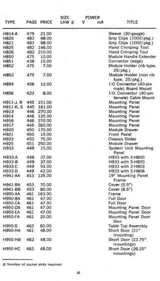
SIZE POWER
TYPE PAGE PRICE LHW
#
V mA TITLE714 378 200.00 +5 7000 Power Supply 728 381 240.00 +10 7500 Power Supply
-15 8500
728A 381 260.00 +10 7500 Power Supply -15 8500
782 374 128.00 +10 400 Power Supply -15 3000
782·A 374 148.00 +10 400 Power Supply -15 3000
783 383 240.00 +10 7500 Power Supply -15 8500
783A 383 260.00 +10 7500 Power Supply -15 8500
911 497 9.00 Patchcords (10/ pkg.)
913 481 25.00 Patchcords (100/ pkg.)
914·7 500 4.00 Power Jumpers
(10/ pkg).
914·19 500 4.00 Power Jumpers
(10/ pkg.)
915 481 33.00 Patchcords (100/ pkg.)
917 483 50.00 Daisy Chain
932 477 .60 Bus Strip
933 477 1.00 Bus Strip
934 477 :50.00 Wire Wrapping Wire
(1000 ft. roll)
935 478 60.00 Wire Wrapping Wire
(1000 ft. roll) 937 476 7.00/pkg. 25 Gray handles per
package
939 478 1.50 Bus Strip
1907 439 9.00 Panel Cover
1945·19 439 20.00 Hold Down Bar
4913 500 25.00 Mounting Racks
12·01954 462 25.00 Mounting Slides
12·09703 462 52.00 Tilt Slides
17·00001 394 1.00/ ft. Cable, Flat Coax "g·conductor
17·00002 394 0.75/ft. Cable, 1.25" Mylar Flat Mylar 10·cond.
17·00003 394 1.50 Cable, Round Coax
9·conductor 70·05909 462 50.00 AC Distribution Panel
74·06782 462 6.00 Kickplate
74·06793 462 8.00 Kickplate
# Number of socket slots required.
SIZE POWER TITLE
TYPE PAGE PRICE LHW
#
V ·mA91-07575 394 0.60/ft. Cable, Ribbon 20-cond.
91-07599 394 2.00/ft. Cable, Twisted pair Coax
36-conductor
91-07722 394 2.001 ft. Cable, Flat 40-conductor
A123 278 58.00 SSS 1 +5 45 Four-Channel
Multi-+10 18 plexer
-20 50
A160 280 150.00 SDD 4 +15 25 High-Impedance
Multi--15 25 plexer Expander
A161 282 200.00 SDD 4 +15 35 High-Impedance
Multi--15 35 plexer with Output
Buffer
A162 285 160.00 SDD 4 +5 30 High-Impedance
Multi-+15 35 plexer with Decoder
-15 35
A163 288 210.00 SDD 4 +5 30 High-Impedance
Multi-+15 35 plexer with Decoder
-15 35 & Buffer
A164 291 175.00 SDD 4 +15 40 Constant Impedance
-15 40 Multiplexer Expander
A165 293 225.00 SDD 4 +15 40 Constant Impedance
-15 40 Multiplexer with
Out-put Amplifier
A166 295 185.00 SDD 4 +5 30 Constant Impedance
+15 40 Multiplexer Expander
-15 40 with Decoder
A167 297 240.00 SDD 4 +5 30 Constant Impedance
+15 40 Multiplexer with
De--15 40 coder & Output
Amplifier
A207 300 45_00 SSS 1 +15 6 Operational Amplifier
-15 10
A260 302 150.00 SDD 4 +15 20 Dual Amplifier Card
-15 20
A404 306 130.00 SDS 2 +15 22 Single Sample & Hold
-15 35 for lO-bit Systems
A460 308 200.00 SDD 4 +15 12 Single Sample & Hold
-15 12 for 12-bit Systems
A461 308 250.00 SDD 4 +15 20 Single Sample & Hold
-15 20 with Input Buffer for
12-bit Systems
A613 310 200.00 SDS 2 +5 60 12-Bit BCD or Binary
+15 35 DAC
-10 7
-15 60
# Number of socket slots required.
SIZE POWER
TYPE PAGE PRICE LHW
#
V rnA TITLEA618 312 125.00 SDD 4 +5 135 10·Bit D/ A Converter,
+10.06 60 Single Buffered
+15 25
-15 85
A619 312 325.00 SDD 4 +5 135 10·Bit D/ A Converter,
+10.06 60 Single Buffered
+15 25
-15 85
A620 314 125.00 SDD 4 +5 190 10·Bit D/ A Converter,
+10.06 60 Double Buffered
+15 25
-15 85
A621 314 125.00 SDD 4 +5 190 lO·Bit D/ A Converter,
+10.06 60 Double Buffered
+15 25
-15 85
A623 316 350.00 SSS 1 +5 315 12·Bit D/ A Converter,
+15 25 Double Buffered
-15 25
A660 318 300.00 SDD 4 +5 45 12·Bit Multiplying D/ A
+15 25 Converter, Straight
-15 25 Binary
A661 320 300.00 SDD 4 +5 45 12·Bit Multiplying D/ A
+15 25 Converter, BCD
-15 25
A662 322 300.00 SDD 4 +5 45 12·Bit Multiplying D/ A
+15 25 Converter, 2's
Com--15 25 plement
A663 324 350.00 SDD 4 +5 125 12-Bit Multiplying D/ A
+15 25 Converter, Buffered
-15 25 Straight Binary
A704 326 184.00 SDS 2 -15 250 Reference Supply
A811 328 350.00 SDD 4 +5 300 lO-Bit A/ D Converter
+15 20
-15 160
A860 330 200.00 SDD 4 +5 150 12-Bit Industrial A/ D
+15 20 Converter
-15 20
A861 333 300.00 SDD 4 +5 420 High-Speed 12-Bit
Uni-+15 55 polar A/ D Converter
-15 12
A862 335 300.00 SDD 4 +5 420 High·Speed 12·Bit
Bi-+15 55 polar A/ D Converter
-15 12
A990 337 4.00 SSD 2 Amplifier Board
A992 337 4.00 SSD 2 Amplifier Board
BBll 471 90.00 System Unit for General
Interfacing
# Number of socket slots required.
SIZE POWER
TYPE PAGE PRICE LHW# V rnA TITLE
BC02F·XX 395 33.00 91·07575 Cable (W01S·
W023)
BC02L·XX 395 30.00 91·07575 Cable (W021·
W021)
BC02M·XX 395 30.00 91·07575 Cable (W021·
W022)
BC02p·XX 395 30.00 91·07575 Cable (W022·
W022)
BC02S·XX 395 30.00 91·07575 Cable (W023·
W023)
BC02W·XX 395 30.00 91·07575. Cable (,;\/022,
W02S)
BC02X·XX 399 5S.00 91·07575 Cable (M90S·
M90S)
BC02Y·XX 395 31.00 91·07575.Cable (WOll·
W021)
BC03A·XX 396 38.00 17·00001 Cable (WOll·
WOll)
BC03B·XX 396 37.00 17·00001 Cable (WOll·
W021)
BC03C·XX 396 36.00 17·00001 Cable
{W021-W021)
BC03D·XX 396 36.00 17-00001.Cable (W021·
W022)
BC03E·XX 397 29.00 17·00002 Cable
(W031-W031)
BC03F·XX 397 2S.00 17·00002 Cable (WO~3·
W033)
BC03J·XX 396 36.00 17·00001 Cable (W028·
W02S)
BC03H·XX 39S 54.00 17·00002 Cable
(M901-M901)
BC04A·XX 395 15.00 91·07575 Cable (WOll·
OPEN)
BC04B·XX 395 lS.00 91·07575 Cable
(W0l8-OPEN)
BC04F·XX 395 15.00 91·07575 Cable (W023·
OPEN)
BC04L·XX 396 lS.00 17·00001 Cable
(WOll-OPEN)
BC04M·XX 396 18.00 17·00001 Cable
(W021-OPEN)
BC04N·XX 396. .lS.00 17-00001 Cable (W022·
OPEN)
BC04p·XX 400 36.00 17·00001 Cable (M904·
OPEN)
BC04T·XX 398 27.00 17-00002 Cable (M901·
OPEN)
# Number of socket slots required.
SIZE POWER
TYPE PAGE PRICE lHW
#
V mA TITLEBC04U-XX 398 22.00 17-00002 Cable
(M903-OPEN)
BC04W-XX 399 28.00 91-07575 Cable
(M908-OREN)
BC04Z 403 See Listing 91-07722 Cable
(H856-OPEN)
BC08A 398 See Listing 17-00002 Cable
(M903-M903)
BC08B 400 See Listing 17-00001 Cable
(M904-M904)
BC08C 398 See Listing 17-00002 Cable
(M903-Two W031)
BC08D 400 See Listing 17-00001 Cable
(M904-Two WOll)
BC08J 401 See Listing 91-07722 Cable
(H856-M953)
BC08K 401 See Listing 91-07722 Cable
(H856-M955)
BC08l 402 See Listing 91-07722 Cable (Two
H856-M954)
BC08R 403 See Listing 91-07722 Cable
(H856-B'CHA
H856)
404 See Listing . 91-56-92-6 Cable
(M919-M929)
Cab A 445 411.00 Cabinet
Cab B 456 431.00 Cabinet
CabC 456 437.00 Cabinet
Cab D 456 390.00 Cabinet
Cab E 457 410.00 Cabinet
Cab F 457 340.00 Cabinet
Cab I 458 476.00 Cabinet
Cab J 458 419.00 Cabinet
Cab K 459 365.00 Cabinet
DECkits 359 See Kits
H001 439 7.00 0.75/1 Mounting
Brackets (pr)
H002 439 15.00 2.00/1 Mounting
Brackets (pr)
H014 447 20.00 Mounting Panel
H019 454 70.00 Mounting Bar
H020 439 15.00 19/1 Mounting Frame
Casting
H021 439 7.00 End Plate
H022 439 20.00 End Plate
H024 439 7.00 End Plate 8.5 inches
H025 439 20.00 End Plate 8.5 inches
with Terminal Block
H500 492 375.00 Computer lab (120 Vac)
# Number of socket slots required.
SIZE POWER
TYPE PAGE PRICE LHW
#
V mA TITLEH500A 492 375.00 Computer Lab (240 Vac)
H510 495 995.00 K Series Logic Lab
H520 503 995.00 MSeries Logic Lab
H701 374 116.00 +10 400 Power Supply
-15 3000
H701·A 374 136.00 +10 400 Power Supply
-15 3000
H704 375 200.00 +15 400 Power Supply
-15 400
H707 375 400.00 +15 1500 Power Supply
-15 1500
H710 377 lS0.00 +5 5000 Power Supply
H716 379 150.00 +5 4000 Power Supply
-15 1500
H726 3S0 200.00 +5 7000 Power Supply
HSOO-F 433 S.OO Connector Block
HSOO-W 433 S.OO Connector Block
HS01-F 433 2.00 Replacement Pins
HS01-W 433 2.00 Replacement Pins
HS02 434- 4.00 . Connector Block
HS03 435 13.00 Connector Block
HS05 435 4.00 Connector Block
HS07 436 5.00 Connector Block
HSOS 437 10.00 Connector Block
HS09 437 4.00 Replacement Pins
HSlO 479 99.00 Hand Wire Wrapping
Tool (24 ga.)
HSlO-A 479 99.00 Hand Wire Wrapping
Tool (30 gao)
HSIO-B 479 150.00 Hand Wire Wrapping
Tool (24 & 30 ga.)
HSIO-C 4S0 150.00 Battery Operated Wire
Wrapgun (24-gauge sleeve & bit)
HSlO-O 4S0 150.00 Battery Operated Wire
Wrapgun (30-gauge sleeve & bit)
HSIO-E 4S0 100.00 Battery Operated Wire
Wrapgun
HS11 479 24.00 Hand Wrapping Tool
HS11-A 479 24.00 Hand Wrapping Tool
HS12 479 10.00 Hand Unwrapping Tool
(24-gauge)
HS12-A 479 10.00 Hand Unwrapping Tool
(30-gauge)
HS13 479 30.00 Bit (24-gauge)
HS13-A 479 30.00 Bit (30-gauge)
HS14 479 21.00 Sleeve (24-gauge)
# Number of socket slots required.
SIZE POWER
TYPE PAGE PRICE LHW
#
v-
mA TITLEH814-A 479 21.00 Sleel(e (30-gauge)
H820 483 48.00 Grip Clips (1000/ pkg.)
H821 483 98.00 Grip Clips (1000/ pkg.)
H825 482 146.00 Hand Crimping Tool
H826 482 210.00 Hand Crimping Tool
H850 475 10.00 Module Handle Extender
H851 438 15.00 Connector (edge)
H852 475 7.00 Module Holder (rib type,
25/pkg.)
H853 475 7.00 Module Holder (non rib
type, 25/ pkg.)
H854 426 12.00 I/O Connector (40-pin
male) Board Mount
H856 423 8.00 I/O Connector (40-pin
female) Cable Mount H91l-J, R 445 151.00 Mounting Panel H91l-K, S 445 161.00 Mounting Panel
H913 446 270.00 Mounting Panel
H914 446 125.00 Mounting Panel
H916 446 270.00 Mounting Panel
H917 446 260.00 Mounting Panel
H920 450 170.00 Module Drawer
H921 450 15.00 Front Panel
H923 450 75.00 Chassis Slides
H925 451 250.00 Module Drawer
H933 449 15.00 System Unit Mounting
Panel
H933-A 449 37.00 H933 with 3-H800
H933-B 449 37.00 H933 with 3-H800
H933-C 449 54.00 H933 with 3-H803
H933-D 449 42.00 H933 with 3-H808
H941-AA 453 125.00 19" Mounting Panel Frame
H941-BA 453 70.00 Cover (5.5")
H941-BB 453 80.00 Cover (8.5")
H950-AA 461 163.00 Frame
H950-BA 461 47.00 Full Door
H950-CA 461 47.00 Full Door
H950-DA 461 47.00 Mounting Panel Door
H950-EA 461 47.00 Mounting Panel Door
H950-FA 461 20.00 Mounting Panel Door
Skin
H950-G 462 60.00 Table Top Assembly
H950-HA 461 48.00 Short Door (21" mounting) H950-HB 462 48.00 Short Door (22.75"
mountings) H950-HC 462 48.00 Short Door (26.25"
mountings)
# Number of socket slots required.
[image:12.385.27.349.0.565.2]SIZE POWER
TYPE PAGE PRICE LHW
#
V rnA TITLEH950-HD 462 4ROO Short Door (31-5" mountings) H950-HE 462 48.00 Short Door (36.75"
mountings) H950-HF 462 48.00 Short Door (42"
mountings)
H950-HG 462 48.00 Short Door
H950-HH 462 48.00 Short Door
H950-HJ 462 48.00 Short Door
H950-HK 462 48.00 Short Door
H950-LA 462 9.00 Frame Panel
H950-LB 462 7.00 Frame Panel
H950-PA 462 ROO Cover Bezel Panel
(5.25")
H950-QA 462 11-00 Cover Bezel Panel
(10.5")
H950-SA 462 4.00 Filter
H952-AA 462 57.00 End Panel
H952-BA 462 23.00 Stabilizer Feet (pair)
H952-CA 462 40.00 Fan Assembly
H952-EA 462 7.00 Caster Set
H952-FA 462 2.00 Leveler Set
H952-GA 462 44.00 Filler Strip
H957-AA 466 142.00 Frame
H957-BA 466 60.00 Full Door Rear Mount (RH)
H957-CA 466 60.00 Full Door Mount (LH)
H957-DA 466 36.00 Mounting Panel
(Plenum) Door, rear mount (RH)
H957-EA 446 36.00 Mounting Panel
(Plenum) Door, rear mount (LH)
H957-FA 466 63.00 End Panel,right hang
H957-FB 466 63.00 End Panel, left hang H957-GA 466 36.00 Filler Strip Group (3)
H957-HA 466 50.00 Fan Assembly (500
CFM)
H957-JA 466 9.00 Bottom Cover Plate
H957-LA 466 20.00 Logo Frame Panel
H957-SA 466 4.00 Filter
H9190 454 250.00 Mounting Panel
See Control Handbook for K Series Modules
K731 385 30.00 SST 3 +5 1000 Source Module K732 387 27.00 SSQ 4 +5 2000 Slave Regulator K741 390 30.00 12_6 1000 Power Transformer K743 390 45.00 12.6 6000 Power Transformer
K771 389 35.00 Display Supply
# Number of socket s,lots required.
SIZE POWER
TYPE PAGE PRICE LHW
#
V rnA TITLEK900 496 185.00 Control Panel-Power
Supply
K901 497 125.00 Patch Board Panel
K902 498 145.00 Indicator Switch Panel
K903 499 155.00 Patch Panel Board
K940 441 6.00 Mounting Support
K941 441 6.00 Mounting Frame
K943·R 444 96.00 Mounting Panel
K943·S 444 96.00 . Mounting Panel
Kit·H 362 See Listing DEC KIT, 1/0,4 Words
IN/4 Words OUT
Kit·F 364 See Listing DEC KIT, I/O, 3 Words
IN/4 Words OUT
Kit·K 365 See Listing DEC KIT, I/O, 8
Words IN
M002 21 10.00 SSS 1 +5 16 Logic HIGH Source
M040 22 39.00 SSS 1 +5 47 Solenoid Driver
-15 9
M050 24 31.00 SSS 1 +5 47 50 rnA Indicator Driver
-15 16
M051 155 31.00 SSS 1 +5 47 Positive to Negative
-15 16 Logic Level Converter
M060 25 55.00 SSS 1 +5 80 Solenoid Driver
M100 156 50.00 SSS 1 +5 60 Bus Data Interface
-15 10
M101 158 24.00 SSS 1 +5 82 Bus Data Interface
M102 160 60.00 SSS 1 +5 130 Device Selector
-15 40
M103 162 45.00 SSS 1 +5 110 Device Selector
M105 164 65.00 ESS 1 +5 338 Address Selector
M107 166 105.00 SDS 2 +5 245 Device· Selector
M108 168 45.00 SSS 1 +5 137 Flag Module
M111 27 22.00 SSS 1 +5 87 Inverter
M112 28 35.00 . SSS 1 +5 50 NOR Gate
M113 30 18.00 SSS 1 +5 71 NAND Gates
M115 30 18.00 SSS 1 +5 41 NAND Gates
M116 29 20.00 SSS 1 +5 30 Six 4·lnput NOR Gates
M117 30 19.00 SSS 1 +5 41 NAND Gates
M119 30 18.00 SSS 1 +5 19 NAND Gates
M121 33 23.00 SSS 1 +5 50 AND/NOR Gate
M133 34 27.00 SSS 1 +5 160 Two·lnput NAND Gates
M135 35 32.00 SSS 1 +5 100 Eight 3·lnput NAND
Gates
M139 36 28.00 SSS 1 +5 50 Three 8·lnput NAND
Gates
M141 37 29.00 SSS 1 +5 117 NAND/OR Gates
M152 39 36.00 SSS 1 +5 265 Dual 1 of 8 Decoder
M155 41 30.00 SSS 1 +5 55 4·Line to 16·Line
Decoder
# Number of socket slots required.
SIZE POWER
TYPE PAGE PRICE LHW
#
V mA TITLEM159 43 35.00 SSS 1 +5 150 Arithmetic/ Logic Unit M160 47 33.00 SSS 1 +5 30 AND/NOR Gate M161 48 55.00 SSS 1 +5 120 Binary to Octal/ Decimal
Decoder M162 50 63.00 SSS 1 +5 102 Parity Circuit M165 51 30.00 SSS 1 +5 130 8 Buffers M168 52 45.00 SSS 1 +5 250 12-Bit Magnitude
Comparator M169 54 33.00 SSS 1 +5 50 Gating Module M191 55 22.00 SSS 1 +5 130 ALU Look-Ahead Logic M202 58 29.00 SSS 1 +5 57 Triple J-K Flip-Flop M203 59 26.00 SSS 1 +5 55 8 R/ S Flip-Flops M204 60 34.00 SSS 1 +5 74 General-Purpose Buffer
& Counter M205 61 33.00 SSS 1 +5 90 General-Purpose
Flip-Flops
M206 62 30.00 SSS 1 +5 87 General-Purpose Flip-Flops
M207 64 33.00 SSS 1 +5 96 General-Purpose Flip-Flops
M208 66 84.00 SSS 1 +5 184 8-Bit Buffer/ Shift Register
M230 68 105.00 SDS 2 +5 860 Binary to BCD & BCD to Binary Converter M232 70 125.00 SSS 1 +5 200 16-Word RAM
M236 72 50.00 SSS 1 +5 330 12-Bit Binary Up/ Down Counter
M237 74 50.00 SSS 1 +5 330 3-Digit BCD Up/Down Counter
M238 76 35.00 SSS 1 +5 180 Dual 4-Bit Binary Syn-chronous Up/ Down Counter
M245 78 28.00 SSS 1 +5 130 Dual 4-Bit Shift Register M246 80 21.00 SSS 1 +5 160 5 D-Type Flip-Flops M248 82 15.00 SSS 1 +5 130 Dual 4-Bit Multipurpose
Shift Register M253 84 73.00 SSS 1 +5 390 16-Word X 12-Bit RAM M260 88 221.00 SDS 2 +5 375 4-Word X 12-Bit
Associa-tive Memory
M261 91 40.00 SSS 1 +5 175 4-State Motor Translator M262 93 65.00 SDS 2 +5 350 lO-State Motor
Trans-lator
M302 95 46.00 SSS 1 +5 166 Dual Delay Multivibrator M306 97 27.00 SSS 1 +5 120 Integrating One Shot M310 99 58.00 SSS 1 +5 89 Delay Line
M360 100 68.00 SSS 1 +5 50 Variable Delay M401 101 55.00 SSS 1 +5 80 Variable Clock
M403 103 30.00 SSS 1 +5 70 RC Multivibrator Clock M404 105 65.00 SSS 1 +5 535 Crystal Clock
M405 106 100.00 SSS 1 +5 50 Crystal Clock # Number of socket slots required.
SIZE POWER
TYPE PAGE PRICE LHW
#
V mA TITLEM410 107 70.00 SSS 1 +5 95 Reed Clock
M452 108 40.00 SSS 1 +5 77 Variable Clock
M500 170 55.00 SSS 1 +5 160 Negative Input/ Positive
-15 64 Output Receiver
M501 109 25.00 SSS 1 +5 31 Schmitt Trigger
M502 172 26.00 SSS 1 +5 49 Negative Input Conver·
-15 92 ter, High·Speed
M506 173 52.00 SSS 1 +5 81 Negative Input Conver·
-15 115 ter, Medium·Speed
M507 175 45.00 SSS 1 +5 42 Bus Converter,
Medium--15 115 Speed
M510 177 51.00 SSS 1 +5 170 I/O Bus Receiver
M521 111 16.00 SSS 1 +5 56 K to M Converter
M602 112 28.00 SSS 1 +5 213 Pulse Amplifier
M606 113 43.00 SSS 1 +5 188 Pulse Generator
M610 115 20.00 SSS 1 +5 41 Open Collector 2-lnput
NAND Gate
M617 117 26.00 SSS 1 +5 97 4·lnput Power NAND
Gate
M622 178 45.00 SSS 1 +5 210 8-Bit Positive Input/
Output Bus Driver
M623 180 40.00 SSS 1 +5 71 Bus Driver
M624 181 45.00 SSS 1 +5 89 Bus Driver
M627 118 29.00 SSS 1 +5 136 NAND Power Amplifier
M632 183 55.00 SSS 1 +5 175 Positive Input Negative
-15 40 Output Bus Driver
M633 185 50.00 SSS 1 +5 100 Negative Bus Driver
-15 40
M650 187 25.00 SSS 1 +5 37 Negative Output
Con--15 29 verter
M652 188 26.00 SSS 1 +5 122 Negative Output
Con--15 202 verter
M660 119 25.00 SSS 1 +5 71 Positive Level Cable
Driver
M661 120 15.00 SSS 1 +5 111 Positive Level Driver
M671 121 52.00 SSS 1 +5 112 M to K Converter
M706 123 150.00 SDS 2 +5 400 Teletype Receiver
M707 128 150.00 SDS 2 +5 375 Teletype Transmitter
M730 190 160.00 SDS 2 +5 400 Bus Interface
M731 190 160.00 SDS 2 +5 400 Bus Interface
-15 90
M732 194 160.00 SDS 2 +5 400 Bus Interface
M733 194 165.00 SDS 2 +5 400 Bus Interface
-15 125
M734 198 105.00 SDS 2 +5 325 I/O Bus Input
Multi-plexer
M735 200 135.00 SDS 2 +5 425 I/O Bus Transfer
Register
M736 203 125.00 SDS 2 +5 400 Priority Interrupt Module
# Number of socket slots required.
SIZE POWER
TYPE PAGE PRICE LHW
#
V mA TITLEM737 207 120.00 SDS 2 +5 300 12-Bit Bus Receiver
Interface
M738 209 105.00 SDS 2 +5 250 Counter Buffer Interface
M783 211 30.00 ESS 1 +5 70 UNIBUS Drivers
M784 212 30.00 ESS 1 +5 200 UNIBUS Receivers
M785 213 35.00 ESS 1 +5 118 UNIBUS Transceiver
M786 214 220.00 EDS2 +5 600 Device Interface
M795 218 200.00 EDS 2 +5 600 Word Count and BUS
Address Module
M796 221 100.00 ESS 1 +5 180 UNIBUS Master Control
Module
M798 224 40.00 ESS 1 +5 320 UNIBUS Drivers
M901 406 15.00 SSS 1 Flat Mylar Cable
Con-nector
M903 406 10.00 SSS 1 Flat Mylar Cable
M904 412 10.00 SSS 1 Coaxial Cable Connector
M906 132 20.00 SSS 1 +5 440 Cable Terminator
M907 226 16.00 SSS 1 +5 10 Diode Clamp
M908 416 10.00 SSS 1 Ribbon Connector
M909 227 14.00 SSS 1 Terminator
M910 228 20.00 SSS 1 +5 1350 Terminator
M912 413 25.00 SDS 2 Coax Cable Connector
M915 406 30.00 SSS 1 Ribbon Cable Connector
M917 416 10.00 SSS 1 Ribbon Cable Connector
Flat Mylar Cable
M918 406 10.00 SSS 1 Connector
M920 356 45.00 SDT 1 UNIBUS Connector
Module
M922 406 6.00 SSS 1 Flat Mylar Cable
Connector
M925 406 9.00 SSS 1 Flat Mylar Cable
Connector
M926 406 27.00 SSS 1 Flat Mylar Cable
Connector
M927 412 6.00 SSS 1 Coax Cable Connector
M935 356 45.00 SSS 1 Internal Bus Connector
M953 423 25.00 SSS 1 Flat Cable Connector
M954 423 27.00 SSS 1 Flat Cable Connector
M955 423 27.00 SSS 1 Flat Cable Connector
M957 416 21.00 ESS 1 Ribbon Cable Connector
M975 428 35.00 SDS 2 Flip Chip to H854
Adapter
Mll03 133 14.00 SSS 1 +5 80 2-lnput AND Gates
M1307 134 12.00 SSS 1 +5 100 4-lnput AND Gates
M1500 229 35.00 ESS 1 +5 300 Bidirectional Bus
Inter-facing Gates
M1501 232 50.00 ESS 1 +5 300 Bus Input Interface
M1502 234 100.00 EDS 2 +5 750 Bus Output Interface
M1510 237 100.00 EDS 2 +5 600 Bus Device Selector
# Number of socket slots required.
SIZE POWER
TYPE PAGE PRICE LWH
#
V rnA TITLEM1621 240 125.00 EQS 4 +5 777 DVM Data Input
Inter-face
M1623 243 150.00 EQS 4 +5 1600 Instrument Remote
Con-trol Interface
MI701 135 17.00 SSS 1 +5 110 Data Selector
M1703 247 75.00 EQS 4 +5 555 OMNIBUS Input
Inter-face
M1709 250 125.00 EQD 8 +5 830 OMNIBUS Interface
Foundation Module
M1713 137 13.00 SSS 1 +5 70 16-Line to I-Line Data
Selector
M1801 254 350.00 EQS 4 +5 1450 16-Bit Relay Output
Interface
M73XX 263 See RTM Listing
M7390 139 275.00 EDS2 +5 700 Asynchronous
Trans-+10 3 ceiver
-15 80
M7820 258 100.00 ESS 1 +5 550 Interrupt Control,
UNIBUS
M7821 260 100.00 ESS 1 +5 725 Interrupt Control,
UNIBUS
M9100 143 30.00 ESS 1 H854 to H854 to Flip
Chip Adapter Power Supplies 369
RT01 486 See Listing Numeric Data Entry
Terminal
RT02 486 See Listing Alphanumeric Data
En-try Terminal
W011 416 6.00 SSS 1 Ribbon Cable Connector
W0l8 416 9.00 SSS 1 Ribbon Cable Connector
W020 416 8.00 SSS 1 Ribbon Cable Connector
W021 416 6.00 SSS 1 Ribbon Cable Connector
W022 416 6.00 SSS 1 Ribbon Cable Connector
W023 416 6.00 SSS 1 Ribbon Cable Connector
W024 412 6.00 SSS 1 Ribbon Cable Connector
W027 416 7.00 SSS 1 Ribbon Cable Connector
W028 412 6.00 SSS 1 Coax Cable Connector
W03l 406 5.00 SSS 1 Flat Mylar Cable
Con-nector
W033 406 5.00 SSS 1 Flat Mylar Cable
Con-nector
W940 341 70.00 EQD 8 Wire Wrappable Module
W941 341 40.00 EDD4 Wire Wrappable Module
W942 341 140.00 EQD 8 Wire Wrappable Module
with Sockets
W943 341 75.00 EDD4 Wire Wrappable Module
with Sockets
W950 341 65.00 EQD 8 Wire Wrappable Module
W951 341 40.00 EDD4 Wire Wrappable Module
# Number of socket slots required.
.' ~;'"o~~
SIZE POWER
TYPE PAGE PRICE LWH
#
V mA TITLEW952 341 140.00 EQD 8 Wire Wrappable Module
with Sockets
W953 341 75.00 EDD4 Wire Wrappable Module
with Sockets
W960 344 8.00 SSS 1 MSI Mounting Board
W964 345 10.00 SSS 1 Collage Universal
Ter-minator
W966 346 85.00 EQD 8 OMNIBUS Wire Wrap
Module
W967 346 165.00 EQD.8 OMNIBUS Wire Wrap
Module with Sockets
W968 347 45.00 EQS 4 Collage Mounting Board
W969 347 30.00 EDS 2 Collage Mounting Board
W970 348 4.00 SSS 1 Blank Module
W971 348 8.00 SDS 2 Blank Module
W972 348 4.00 SSS 1 Blank Module
W973 348 6.00 SDS 2 Blank Module
W974 348 9.00 SSS 1 Blank Module
W975 348 18.00 SDS 2 Blank Module
W979 351 20.00 SDS 2 Collage Mounting Board
W980 352 14.00 SSS 1 Module Extender
W982 353 18.00 ESS 1 Module Extender
W984 354 30.00 EDS2 Module Extender
W987 355 40.00 EQS 4 Quad Module Extendei
W990 349 2.00 SSS 1 Blank Module
W991 349 5.00 SDS 2 Blank Module
W992 349 2.00 SSS 1 Blank Module
W993 349 4.00 SDS 2 Blank Module
W998 349 4.00 SSS 1 Blank Module
W999 349 9.00 SDS 2 Blank Module
W9720 357 6.00 ESS 1 Blank Module, Copper
Clad on both sides
W9721 357 8.00 EDS 2 Blank Module, Copper
Clad on both sides
W9722 357 13.00 EQS 4 Blank Module, Copper
Clad on both sides
# Number of socket slots required.
This ninth edition of the LOGIC HANDBOOK is your guide to the most exten-sive line of products offered by Digital Equipment Corporation for implement-ing electronic logic designs for instrumentation, computer interfacimplement-ing, data gathering or control. This handbook is a basic reference for anyone involved in specifying, manufacturing or using solid-state logic.
Our M Series TTL integrated circuit modules are featured in this edition. The M Series line consists of more than 100 modules ranging from basic and fundamental logic modules to self-contained computer interfacing modules and the M Series Logic Lab for use in breadboarding M Series logic designs. The impact of advancing technology can be seen in M Series evolution. From the beginning, M Series was TTL-integrated, circuit-oriented; the current trend is toward MSI and LSI. The result is more complexity (and more built-in de-sign solutions) per module. Many of the modules in this handbook amount to full-scale digital subsystems_
Further versatility has been added to the M Series line by the availability of three Interfacing Kits, described herein. The kits offer the user the capability of implementing more complex input/output interfacing between a PDP-ll computer and peripheral equipment at low cost and. minimum design time. A new design concept has been made available to the designer of digital systems with the availability of RT Modules listed in this handbook. These modules, using the Register Transfer concept, cut design time drastically, reduce documentation and demand only a fundamental knowledge from the system designer.
This edition of the handbook also covers the A Series of analog modules, the W Series of wire wrappable modules, collage and blank boards in the FLIP CHIP form factor, and a complete line of power supplies and hardware. An expanded section on cabling and cable accessories has been added to sim-plify system interconnection design. All these support functions provide a total capability for designing, implementing, and assembling a modular sys-tem, small or large, at the lowest cost per function in the industry.
A new dimension has been added to this edition with the inclusion of two popular data entry terminals. These are the RTOI Numeric Data Entry Ter-minal and the RT02 Alphanumeric Data Entry TerTer-minal. Both terTer-minals imple-ment low-cost applications in the areas of manageimple-ment information systems, medical and clinical laboratories, industrial and production monitoring, bank-ing transactions.
Extensive noncatalog products and services are available from DIGITAL. If you require unique functions that are not listed in this handbook, contact your local DIGITAL office (listed inside the back cover). The product you need may be available as a noncatalog item. In addition, DIGITAL. maintains a Special Module Products Group with complete capability of design, layout, manufacturing and test. Custom product capability is not limited to modules alone but extends to the support hardware and accessories, including cabling, wire wrapping and cabinets.
A worldwide staff of DIGITAL sales engineers is prepared to respond to your technical and commercial needs. From a backlog of logic system design ex· perience, DIGITAL may have a detailed solution to your application or inter-.; face requirement.
Please address - any comments on:,this handbook, or inquiries concerning special services, to:
xx
Digital Equipment Corporation 146 Main Street
Maynard, Massachusetts 01754
Attn: Logic Products
ORGANIZATION OF HANDBOOK
This edition of the LOGIC HANDBOOK is organized in eight functional sec-tions for maximum ease of reference. With each section, module descrip-tions are, presented in alphanumeric order by module designation. To locate a specific module, consult the Product List at the beginning of the handbook.
Logic and Control: This section includes all of the M Series basic logic mod-ules and those complex functional modmod-ules that are not computer-interface oriented. An introduction to this section describes the basic characteristics of the TTL integrated circuits which are the principal active elements of M Series.
Computer Interfacing: This group includes the M Series complex functional modules that simplify interfacing to the PDP-ll UNIBUS or PDP-8/e, 8/m OMNIBUS. Also in this group are the mod1Jles for interfacing the external I/O bus of earlier PDP-8 family computers plus level converters and other interface-oriented support modules. Introductory information defines the con-trol an,d data signals of the OMNIBUS, UNIBUS, and external I/O bus .
. Analog: The A Series of analog modules supports the M Series by providing 'a two-way translation between continuously varying real-world voltage mea-surements and the digital realm of control and computation. The present A Series emphasizes 10- and 12-bit performance in a family of mutually compatible functions-multiplexers, operational amplifiers, sample-and-hold circuits, D/ A and A/ D converters, reference voltage sources and an expanded group of multiplying D/ A converters.
Accessory Modules: DIGITAL offers a wide line of wire wrappable, collage, and blank modules in the FLIP CHIP form factor for experimenting and bread-boarding by users who want to work directly with discrete components and integrated circuit packages. Included in this section are module extenders and PDP-8/e, 8/m OMNIBUS bus connectors.
DECkits: These kits offer greater interfacing capability to the PDP-11 UNI-BUS at the lowest cost possible. Complex logic module building block con-cepts are now expanded to greater limits of versatility in kit form. Capable of performing a highly complex computer interface, the /lit is a collection of logic modules assembled by the user to a prewired system unit.
Power Supplies: This section describes a wide selection of Hand K Series dc power supplies for small and large systems. Summary tables are included that will help the system designer select the power supply appropriate to his system.
Cabling: This edition of the handbook presents a greatly expanded section on M and W Series cables and cabling accessories. DIGITAL offers a complete line of prefabricated cables for interconnection of free-standing logic systems as well as computer-based installations_ Bulk cables and cable cards are available so that the user can design and construct his own custom inter-connections with a minimum of custom design and planning.
Hardware: DIGITAL makes a complete line of hardware accessories to support its module series. Module connectors are available for as few as one module to as many as 64 in a single 19" mounting panel. A complete line of cabinets is available to house the modules and their connector blocks, as well as provide a convenient means for system expansion. Wiring accessories and a complete selection of support hardware simplify all phases of-physical construction. This edition's hardware selection is expanded to include the latest cabinet and hardware features.
Data Entry Terminals: This section describes Data Entry Terminals which provide easy, low-cost access to total information in a computer. They offer ideal communication links in numerous situations that require interactive communication between both local and remote operators and the central data processor.
Typical applications are: Stockroom Inventory Control, Management Infor-mation, Production Line Monitoring, Security Systems, Credit Checking, Bank-ing Transactions.
The terminals feature Teletype and EIA serial line compatibility. Interface to a computer is accomplished via a standard full-duplex 4-wire data commu-nications Teletype interface. Standard interfaces are available for the PDP-a, -10, -11, -12, -15, and -16 computers. Modem interface signals corresponding to EIA RS-232C specifications are also provided.
lab Series: This group includes the COMPUTER LAB digital logic trainer, the K Series Logic Lab (a rack-mounted, plugboard-panel breadboarding and training facility for K Series modules) and the M Series Logic Lab (a console and rack structure that mounts and interconnects M Series modules for training, experimentation, and system design).
M SERIES MODULE SELECTOR GUIDE
Available as a com'panion to this handbook is the M Series Module Selector Guide, a. pocket-sized chart that is used for a quick look-up of the charac-. teristics of the M Series modules and the most important supporting hard-ware and accessories and power supplies in this handbook_. Contact your local DIGITAL Sales Office for a free copy of the Module Selector Guide.
DIGITAL EQUIPMENT CORPORATION ENGINEERING SERVICES
In addition to supplying a complete line of standard and special hardware and accessories, Digital Equipment Corporation also provides an engineering, design and manufacturing service in support of customer applications_ These services are available upon request and consist of the following:
Special Logic Modules: Many of the same advanced manufacturing and test-ing techniques which DIGITAL employs to produce its standard modules are applied to building special modules. DIGITAL engineers can provide full module design and development services or they can work with user-supplied drawings and parts lists, depending upon user needs.'
Wire Wrapping: Using the latest in automatic wire wrapping equipment, DIGITAL can efficiently wire and check connector panels according to customer-supplied wire list and specifications.
Special Cables: When standard cables and cable lengths are not applicable to customer requirements, DIGITAL offers a complete cable fabrication ser-vice to build special cables according to customer specifications.
Interface Design: DIGITAL maintains a staff of experienced applications engi-neers who are capable of designing or providin~ design information for in-terfacing DIGITAL computers to custom control systems and, equipment_
Logic Arrays: Special-pu'rpose logic systems can be efficiently designed and built from customer-supplied data. DIGITAL's capability extends from limited production system to high-volume production and insures both optimum design and high reliability at a reasonable cost to the customer_
SPECIAL SYMBOLS AND ABBREVIATIONS
Logic symbols used in this handbook conform, in general, to widely accepted MIL standards. All basic M Series logic symbols (AND, OR, NAND, NOR, Inverter, Flip:Flop) are described in the introduction to the M Series logic and control modules.
Input Loading and Output Drive
On the logic diagrams of this handbook, input and output loading, expressed in TIL unit loads, appear in boxes terminating each input or output signal line_ In the 2-input NAND gate example of Figure 1, both inputs (pins Al and 81) present one TIL unit load_ The output (pin Cl) is capable of driving 10 TIL unit loads. The arrows eliminate any possible confusion as to the direction of signal flow.
INPUT LOADING PIN NUMBER (I TTL UNIT LOAD) /(PIN A,SIDE 1)
AI \ (10 TTL UNIT LOADS) \
/ ,OUTPUT DRIVE
~"~~.
C1@] [image:25.385.42.352.236.500.2]ARROWS SHOW DIRECTION OF SIGNAL FLOW
Figure 1. Logic Diagram Input Loading and Output Drive Symbols
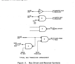
Bus Drivers and Receivers
Drivers and receivers that transfer data along the bidirectional transmission lines of the PDP·8/e, 8/m OMNIBUS or the PDp·ll UNIBUS differ somewhat from similar TTL NAND gates or inverters. Typical examples are shown in Figure 2. The "B" in the loading box indicates that the driver or receiver circuit is to be connected to an OMN IBUS or UN IBUS signal or control line. In this application, unit loading need not be considered. "R" identifies a line receiver and "0" identifies a line driver. Inputs to line receivers or drivers may also be standard TTL levels, in which case, TTL unit loads are shown as usual in the loading box.
DATA TO BUS
B U2
DRIVE TO BUS
~
IB R 7 GATED. BUS
RECEIVER
E1 2
_ _ _ _
~BUSDRIVER
READ FROM BUS
DATA FROM BUS
TYPICAL BUS TRANSCEIVER ARRANGEMENT
Figure 2. Bus Driver and Receiver Symbols
Electrical characteristics of these circuits are described in the introduction to M Series Computer Interfacing Modules.
Level Converters
Whenever logic levels are translated from one set of voltages to another, the conversion is shown taking place in a square level-converter symbol. Inside the box, the corresponding logic levels are related in a simple truth table_ The example of Figure 3 shows a level converter stage that accepts TTL levels (LOW and HIGH) and delivers DEC negative voltage levels (-3 V and ground)_
Input loading is two TTL unit loads_ Whenever loading is peculiar, it is de-fined in a note on the drawing as in the output of Figure 3_
'2lD2 _
n _
01 fjf1~
[image:26.378.34.341.250.489.2]*'SINKS 20mA AT GROUND
Figure _ 3_ Typical Level Converter
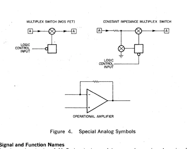
Special Analog Symbols
Symbols used on analog circuit drawings to represent multiplex switches and operational amplifiers are shown in Figure 4_ Loading boxes for analog inputs and outputs contain the letter "A"; do not connect such signals to logic levels_
MULTIPLEX SWITCH (MOS FET)
~
. ALOGIC CONTROL INPUT
CONSTANT IMPEDANCE MULTIPLEX SWITCH
LOGIC
CONTROL---' INPUT
OPERATIONAL AMPLIFIER
Figure 4_ Special Analog Symbols Signal and Function Names
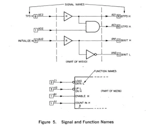
Inputs and outputs of M Series logic modules may be assigned a signal name, a function name, or both_ (See Figure 5.) Signal names appear
out-side blocks or logic symbols to identify typical input or output signals_
_ _ - - - SIGNAL NAMES - -_ _ _ _ _ _
(PART OF M1510)
3 CI
3 f-'V-=-2 _ _ _ .qg~ ~
I"S,,-I _---lENASLE H
I"A::..I _---lCOUNT IN H
J
_ _ -'--.... ---'A~N--jl @)SINITH
X;~-,--_-"A,-"N2=j1O SINIT L
(PART OF M236)
Figure 5. Signal and Function Names
Digital Equipment Corporation uses standard terminology to name signal lines to aid the reader in determining their active state. Either an H or L follows the signal name mnemonic, separated by a space. This letter indio cates the asserted (true) state of the signal. An H means the signal is as-serted when HIGH (+3 V) and an L means the signal is asserted when LOW (0 V). For example, a UNIBUS data line is called BUS 000 L and a grant line is called BUS BG4 H.
On the logic diagrams of many computer interfacing modules iri this hand-book, signal names peculiar to one computer, such as the PDp·11, appear as an example of typical usage. Signal names may be changed to those of another computer or interfacing device if logically appropriate.
Function names appear inside the blocks of functional modules. They iden-tify the function of input or output signals. The user may add his own signal names.
Abbreviations
Abbreviations used in signal and function names in this handbook are de· fined in Table 1.
[image:27.382.36.340.10.267.2]ABBREVIATIONS
ALTN AMPL ANLG BPS CAP CLR CMPR COM CO NT CVRSN DAC EXT GND
H
INIT INT,INTR INTL L OUT-Pol. POT PRGM REF RTN SER SoHo TRIG
Table l-Abbreviations
DEFINITION
Alternate Amplifier Analog Bits Per Second Capacitor Clear Compare Common Control Conversion
Digital to Analog Converter External
Ground
High (TTL +3 V Logic Level) Initialize
Interrupt Internal
Low (TTL 0 V Logic Level) Output
Program Interrupt Potentiometer Program Reference Return Serial
Sample and Hold Trigger
><
~:
8.430:!:·OIO (EXT.LGTH.) .Z19 ::!:.OIO .061 :!:.OIOI. I0.457;g~~ '1
(QUAD. HGT,)
I. 5.IB7~:g~~----_
(OCXJBLE HGTJ
1---+--,--5.250
..-ri
-1
I,· I,. (D~~~:~G~
7.438.
(EXT. LGTH.)
--
I
, - - - - + +
--r-
---1
10312.. _ _ _
.. m
1---
(QUAO HGT)I
3938* (SID LGTH)
180 TYP.
NOTES:
DIMENSIONS DENOTED BY .. ARE FDA
MAX. USEABLf CIROJIT AREA. UNLESS OTHERWISE SPECIFIED ALL
DIMENSIONS ARE ::!: .005",
.128DIA~:gg~ HANDLE HOLES
BOTTOM OF FINGERS
TO TOP OF HANDLE
B.94::!:·olo (EXT. LOTH)
5.50::!:·010 (STD. LGTH)
--l
I :
: I
I :
_"J
j;;;'W"TH
COMPONENT LIMIT:CONCUCTIVE-,B34 NONCONctlCTNE-.875
SINGLE WIDTH
C().4POOENT LIMIT:
CONDt.ICTIVE-.343~
NONCONCUCTIVE -.375~
o
'mLc::>~
". .
''''~~
"'logic
and
. control modules .
DEC Module assembly lines combine automated manufacturing steps with visual inspection and computer controlled testing.
M-SERIES LOGIC AND CONTROL MODULES
Modules in this section appear in numerical order. The six functional cate-gories of M-Series logic and control modules are:
MIll MIl2 M113 M115 M116 M117 M119 M121 M133 M135 M139 M141 M160 M169 M610 MI103 MI307 MI70I MI65 M202 M203 M204 M205 M206 M207 M208 M232 M245 M246 M248 M253 M260 M302 M306 M310 M360 M401 M403 M404 M405 M410 M452 GATES Inverter NOR Gates NAND Gates NAND Gates NOR Gates NAND Gates NAND Gates AND/NOR Gates Input NAND Gates NAND Gates NAND Gates NAND/OR Gates AND/NOR Gates Gating Module
Open Collector NAND Gates AND Gates
AND Gates Data Selector
FLIP-FLOPS
8 Buffers
Triple J-K Flip-Flop 8 R/ S Flip-Flops
General-Purpose Buffer & Counter General-Purpose Flip-Flops General-Purpose Flip-Flops General-Purpose Flip-Flops 8-Bit Buffer/ Shift Register 16-Word RAM
Shift Register 5 D-Type Flip-Flops Multipurpose Shift Register 16-Word X 12 Bit RAM Associative Memory .
TIME RELATED
Dual Delay Multivibrator Integrating One Shot Delay Line
Variable Delay Variable Clock RC Multivibrator Clock Crystal Clock
Crystal Clock Reed Clock Variable Clock
M501 M521 M602 M606 M671 M152 M155 M159 M161 M162 M168 M191 M230 M236 M237 M238 M1713 M040 M050 M060 M617 M627 M660 M661 M002 M261 M262 M706 M707 M906 M7390 M9100 Schmitt Trigger K to M Converter Pulse Amplifier PulsE;! Generator M to K Converter
NUMERIC
Dual 1 of 8 Decoder 4 Line to 16 Line Decoder Arithmetic! Logic Unit
Binary to Octal Decimal Decoder Parity Circuit
12-Bit Magnitude Comparator ALU Look Ahead
Binary to BCD & BCD to Binary Converter 12-Bit Binary Up! Down Counter
3-Digit BCD Up!Down Counter Synchronous Up! Down Counter 16 Line·to·Line Data Selector
LOGIC AMPLIFIERS
Solenoid Driver Indicator Driver Solenoid Driver
4·input Power NAND Gates NAND Power Amplifier Positive Level Cable Driver Positive Level Driver
MISCELLANEOUS
Logic HIGH Source 4·State Motor Translator 10·State Motor Translator Teletype Receiver Teletype Transmitter Cable Terminator
Asynchronous Transceiver 854 to 854 Flip Chip Adapter
M Series modules contain high speed TTL logic in both general purpose and functional logic arrays. TTL was chosen for its high speed, capacitance drive capability, high noise immunity and choice of logical elements, High per· formance integrated circuit modules are now available at approximately one half the price of their discrete or hybrid counterparts.
In addition to the reduced cost of integrated circuits, Digital's advanced manufacturing methods and computer controlled module testing have reo suited in considerable production cost savings, reflected in the low price of all M Series Modules.
GENERAL CHARACTERISTICS
M Series high-speed, monolithic integrated circuit logic modules employ TTL (transistor-transistor logic) integrated circuits which provide high speed, high fan out, large capacitance drive capability and excellent noise margins_ The M Series includes a full digital system complement of basic modules which are designed with sufficient margin for reliable system operation at frequencies up to 6 MHz. Specific modules may be operated at frequencies up to 10 MHz. The integrated circuits are dual in-line packages.
The M Series printed circuit boards are identical in size to the standard FLIP CHlpTM modules. The printed circuit board material is double-sided pro-viding 36-pins in a single height module. Mounting panels (H91O and H911) and 36-pin sockets (H803 and H808) are available for use with M Series modules_ Additional information concerning applicable hardware may be found in the Power Supply & Hardware and Accessories section of this handbook.
M Series modules are compatible with Digital's K Series and, through the use of level converters, are compatible with all of Digital's other standard negative voltage logic FLIP CHIP(ii) modules.
TTL NAND GATE
The basic gate of the M Series is a TTL NAND GATE. Figure 1 is the basic two input NAND gate schematic diagram. The circuit is divided into 3 major sections, the multiple emitter input, the phase splitter and the totem pole output circuit. The two diode model of a transistor shown in Figure 2 will be used in the analysis of the circuit. A forward biased silicon junction (i.e. diode) gives a voltage drop of about 0.75 volts and a saturated silicon transistor has a collector emitter voltage of 0.4 volts average. These two figures will be used througbout the following discussion.
With either input at the LO logic level (0.OV-0.8V) the multiple emitter input transistor will be ON with its base residing at about 0.75
+
0.4=
1.15 volts_ The three diode string consisting of Q,'s base collector diode, Q,'s base emit-ter diode, and Q/s base emitemit-ter diode will have only 1.15 volts across it and will therefore be conducting only leakage currents (0.75+
0.75+
0.75=
2_25 volts required for forward bias). With no current flowing into the base emitter junction of Q" the transistor will be OFF and its collector emitter voltage is alowed to rise. Similarly with no current flowing in the base emitter diode of Q, the transistor is OFF and its collector emitter voltage is allowed to rise. When both Q, and Q. are OFF, Q, is freed to pull the output voltage to a HI level. The voltage levels present in the circuit with one or more LO.in-puts is shown in Figure 4.~---.---~---+5V
4K 1.6K 130 ..
Q3
INPUT A ---~~L_..),...----_1H Q2
' " - - - OUTPUl INPUT B ___________ ...1
Q4
1K
L-__________ 4-___________ GROUND MULTIPLE
. EMITTER
INPUT
PHASE SPLITTER
TOTEM POLE OUTPUT
Figure 1 TIL NAND Gate Schematic Diagram
COLLECTOR
BASE BASE
---__<C>
EMITTER
Figure 2 Two Diode Model For Transistor
+5V
CURRENT PATH
Q2BE Q4BE
• - - - o.75V - - ~
INPUT A ---....1..jo...!!II::::::=<~:.:....;.~_d....;.--__t~----_oI_----__,
Q1
INPUT B (LOW). l _________ .J I
Figure 3 Diode Equivalent NANDGateCircuikOne Input LO
r---~~----~~---+,v
INPUT A
-HIGH
4K
INPUT e - - - . . . J
LOW{Q.4VI
MULTIPLE
EMITTER
INPUT
t6K 130A.
03
~--"3,,.,V,----_ _ _ _ OUTPUT
04
~----~~---G~D
PHASE
SPLITTER
TOTEM POLE
[image:36.382.33.337.0.576.2]OUTPUT
Figure 4 TTL NAND Gate Schematic Diagram, One Input La
+,v
4K
PATH
l
CURR:NTINPUT A -'-",,'Go;"-j<>---+;;:2"'2''''V:='--<>I----<>Ir---<>I---,
If.E'UT B ---'"::.:'G::;"-j<>-_ _ -'
Figure 5 Diode EquivalentNAND Gate Circuit, Both Inputs HI
INPUT A - - - > L
HIGH (2-.4V!
INPUT B _ _ _ _ _ ...J HIGHt2.4V}
r---~~----~---+5V
4K
MULTIPLE
EMITTER
INPUT
t.6K 130.n..
03
~_~O~.4~V _ _ _ OOT~T
04
L---~~---G~ND
PHASE
SPI..JTTE"R TOTEM POLE
OUTPUT
OPERATING CHARACTERISTICS
Power Supply Yoltage: 5 Volts ± 5
%
Operating Temperature Range: 0° to 70°C
Speed: M Series integrated circuit modules are rated for operation in a sys-tem environment at frequencies up to 6 MHz_ Specific modules may be oper-ated at higher frequencies as indicoper-ated by the individual module specifica-tions.
LOGIC LEVELS AND NOISE MARGIN
A gate input will recognize 0_0 volts to 0.8 volts as logical LO and 2.0 volts to 3.6 volts will be recognized as a logical HI. An output is between 0.0 volts and 0.4 volts in the logical LO condition. The logical HI output condition is between 2.4 volts and 3.6 volts. Figure 7 shows diagrammatically the accept-able transistor-transistor logic levels. The worst case noise margin is 400 millivolts that is, an output would have to make at least a 400 millivolt excur-sion to cause an input which is connected to it to go into' the indetermined voltage region. For instance if an output were at 0.4 volts (worst case logical LO) there would have to be a
+
400 mv swing in voltage to cause inputs connected to it to go into their indetermined region.Input and Output Loading: The input loading and output drive capability of M Series modules are specified in terms of a specific number of unit loads. Typica,lly the input loading is one unit, however certain modules may contain inputs which will present greater than one unit load. The typical M Series module output will supply 10 unit loads of input loading. However. certain module 'outputs will deviate from a 10 unit load capability and provide more or less drive. Always refer to the individual module specifications to ascer-tain actual loading figures.
Unit Load: In the logic 0 state, one unit load requires that the driver be able to sink 1.6 milliamps (maximum) from the load's input circuit while main-taininganoutput voltage of equal to or less than +0.4 volts. In the logic 1 state, one unit load. requires that· the driver supply a leakage current 40 microamps ·(maximum) while maintaining an output voltage of equal to or greater than +2.4 volts.
Timing: M Series pulse sources provide sufficient .pulse duration to trigger any M Series flip-flop operating within maximum propagation delay specifi· cations. Detailed timing information appears later in this section and in the module specifications.
INDETERMINED REGION
Figure 7 Logic Levels
NAND logic Symbol: Logic symbology used to describe M Series modules is based on widely accepted standards. Logic symbols and a truth table for the NAND gate are shown in Figure 8.
A~OUTPUT
9~- A:s
A B OUTPUT'
L L H
L H H
A
~
OUTPUTB~A+8
H L H
H H L
Figure 8 NAND Gate Logic Symbol and Truth Table
The first symbol is visually more effective in applications where two high in· puts are ANDed to produce a low output. The second symbol better repre-sents an application where low inputs are ORed to produce a high output.
TTL AND/NOR GATE
r---~----~---~~---o +vcc
A
B
C
D
Q6
Q3
.,_---0 OUTPUT
Figure 9 TTL AND/NOR Gate Simplified Schematic
Circuit Operation: The basic elements of the TTL NAN D gate are used with-out modification_ The phase-splitter (Q2) is paralleled with an identical transistor (Q6), also controlled by multiple-emitter input transistor which receives two additional inputs, C and D_ When either of the, input pairs are high, the phase inverter operates to switch the output voltage low_ Circuit performance is essentially identical to the TTL NAND circuit.
AND/NOR Logic Symbol: The logic symbols for the AND/NOR gate are shown and defined in Figure 10_
A~
.B , OUTPUT
C AB +CD
D
A B C D OUTPUT
H I H ANY L
ANY H H
L H L H
A~
BOUTPUT
~ (A+SI(C+DI
L H H L H H L H L
H L L H
Figure 10 AND/NOR Gate Logic Symbols and Truth Table
NOR Configuration: The AND/NOR gate can perform a straight NOR function if the AND gate inputs are tied together as shown in Figure 11.
A~
OUTPUTB~
: =L>--
OUTPUT AND/NOR INPUTS TIED RESULTING NOR SYMBOLFigure 11 NOR Connection of AND/NOR Gate
NAND GATE FLlp·FLOPS
. RS Flip·Flop: A basic Reset/Set flip-flop can be constructed by connecting two NAND gates as shown in Figure 12_
SET.--~
PREVIOUS INPUT
RESULT STATE CONDITION
1 0 SET RESET 1 0
L H L H H L H L H L L H L H. H H NO CHANGE H L H H NO CHANGE H L L H NO CHANGE
o
L H H L N" r:HANGE RESET---<YL H L L H* H* H L L L H* H*
*Ambiguous state: In practice the input that stays low longest will assume control.
Figure 12 . RESET/SET NAND Gate Flip-Flop
• CLOCKED NAND GATE FLlP·FLOPS
The Reset-Set flip-flop can be clock-synchronized by the addition of a two-input NAND gate to botti-the set and the reset two-inputs_ (See Figure 13_) One of the inputs of each NAN D is tied to a common clock or trigger line_
SET.
CLOCK
o RESET
Figure 13 Clocked NAND Gate Flip-Flop
[image:40.380.23.333.21.307.2]A change of state is inhibited until a positive clock pulse is applied. The ambiguous case will result if both the set and reset inputs are high when the clock pulse occurs.
M SERIES GENERAL-PURPOSE FLIP-FLOPS
Two types of general·purpose flip-flops are available in the M Series, both of which have built-in protection against the ambiguous state characteristic of NAND gate flip-flops.
FLIP-FLOP CLOCK INPUT SYMBOLS
The 0 type flip·flop is a true leading (positive going voltage) edge triggered flip-flop and the 0 input is locked out until the clock input returns to low. The symbol to indicate this function will be as follows;
D TYPE FL I P FLOP CLOCK
The operation of the J-K type flip·flop is to transfer the information present at the J and K inputs just prior to and during the clock pulse to the master flip·flop when the threshold is passed on the leading (positive going voltage) edge of the clock pulse. The information stored in the master flip-flop is transfered to the slave flip-flop, and consequentially to the outputs, when the threshold is passed on the trailing (negative going voltage) edge of the clock pulse. The symbol to indicate this function will be as follows;
J K TYPE FL IP FLOP CLOCK
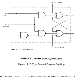
D Type Flip-Flop: The first of these is the 0 type flip·flop shown in Figure 14 In this element, a single-ended data input (D) is connected directly to the set gate input. An inverter is provided between the input line (D) and the reset input. This ensures that the set and reset levels cannot be high at the same time.
D S
C.! 0 R
LOGIC SYMBOL
0---...---1
(SET)
C ---~---~
(CLOCK)
I
I
I
I
L
NAND GATE EQUIVALENT
S (DC SET)
}--+---o
I
---~
R (DC RESET)
SIMPLIFIED NAND GATE EQUIVALENT
Figure 14. D Type General Purpose Flip-Flop
The flip-flop proper employs three-input NAND gates to provide for dc set and reset inputs.
D tYPe flip-flops are especially suited to buffer register, shift register and binary ripple counter applications. Note that D type devices trigger on the leading (or positive going) edge of the clock pulse. Once the clock has passed threshold, changes on the D input will not affect the state of the flip-flop due to a lockout circuit (not shown).
A characteristic of the D type flip-flop which is not illustrated in the NAND gate equivalent circuit is the fact that the D input is locked out after the clock input threshold voltage on the leading (positive going voltage) edge of the clock has been passed_ The D input is not unlocked until the clock input threshold voltage of the trailing (negative going voltage) edge has been passed.
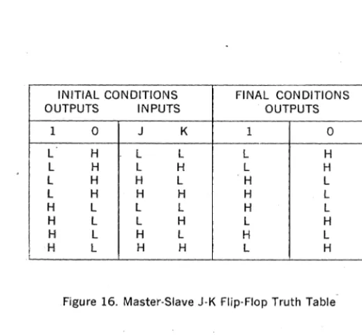
[image:42.387.30.318.41.335.2]· "MASTER-SLAVE J-K FLIP-FLOP"
The two unique features of a J-K flip-flop are: A) a clock pulse will not cause any transition in the flip-flop if neither the J nor the K inputs are enabled during the clock pulse, and B) if both the Jandthe K inputs are enabled during the clock pulse, the flip-flop will complement (change states). There is no indeterminate condition in the operation of a J-K flip-flop.
A word of caution is·in.order concerning the clock input. The J and K inputs must nor-be allowed to change states when the clock line is high, the output will complement on the negative going voltage transition of the clock. It is for this reason that the clock line must be kept low until it is desired to transfer information into the· flip-flop and no change in the states of the J and K inputs should be allowed when the clock line is high.
The J-K flip-flops used are master-slave devices which transfer information to the outputs on the trailing (negative going voltage) edge of the clock pulse. The J-K flip-flop consists of two flip-flop circuits, a master flip-flop and a slave flip-flop. The information which is present at the J and K inputs when the leading edge threshold is passed and during the clock high will be passed to the master flip-flop (The J and K inputs must not change after the leading edge threshold has been passed). At the end of the clock pulse when the threshold of the clock is passed during the trailing (negative going voltage) edge, the information present in the master flip-flop is passed to the slave flip-flop. If the J input is enabled and the K input is disabled prior to and during the clock pulse, the flip-flop will go to the "1" condition when the trailing edge of the clock occurs_ If the K input is enabled and the J input is disabled prior to and during the clock pulse, the flip-flop will go to the "0" condition when the trailing .edge of the clock pulse occurs. If both the J and K inputs are enabled prior to and during the clock pulse, the flip-flop will complement when the trailing edge of the clock pulse occurs. If both the J and Kinputs are disabled prior to and during the clock pulse, the flip-flop will remain in whatever condition existed prior to the clock pulse when the trailing edge of the clock pulse occurs.
J INPUT ----+--j
I OUTPUT
CLOCK
[image:43.387.31.353.156.560.2]o OUTPUT K INPUT - t - - - - l
Figure 15. Master-Slave J-K Flip-Flop