EK-OZQ11-UG-001
DZQ11 Asynchronous
Multiplexer
User's Guide
First Edition, August 1984
Copyright © 1984 by Digital Equipment Corporation
All Rights Reserved
The information in this document is subject to change without notice. Digital Equipment CotpOration assumes no responsibility for any errors herein.
Printed in U.S.A.
The following are trademarks of Digital Equipment Corporation.
mamaamo™
DECDECmate DECUS DECwriter DIBOL MASSBUS
PDP
P/OS
Professional Rainbow RSTS RSX
RT UNIBUS VAX VMS VT
CONTENTS
Page
CHAPTER 1 GENERAL DESCRIPTION
1.1 1.2 1.2.1 1.2.2 1.2.3 1.3 1.3.1 1.3.2 1.3.3 1.3.3.1 1.3.3.2 1.3.3.3 1.3.3.4 1.3.3.5 1.3.3.6 1.3.3.7 1.3.4 1.3.4.1 1.3.4.2 1.3.4.3
INTRODUCTION ... 1-1 PHYSICAL DESCRIPTION... 1-3 DZQl1 Configurations.. . . . .. .. .. . .... .. . .. ... ... ... .. ... .... 1-4 Interface Cables ... 1-6 Test Connectors ... 1-6 SPECIFICATIONS ... 1-8 Environmental . . . 1-8 Electrical ... 1-8 Performance ... 1-8 Interfaces ... 1-8 Maximum Configurations ... 1-8 Throughput ... . . . . 1-9 Receivers .. . . 1-9 Transmitters ... 1-9 Baud-Rate Generator ... 1-9 Performance Summary. .. ... ... .... 1-9 Interrupts ... 1-10
Receiver-Done Interrupt ... 1-10 Silo-Alarm Interrupt ... 1-10 Transmit Interrupt . . . 1-10 CHAPTER 2 INSTALLATION
2.1 2.2 2.3 2.3.1 2.3.2 2.3.3 2.3.4 2.4 2.5
SCOPE ... . UNPACKING AND INSPECTION ... . INSTALLATION PROCEDURE ... . Modem Control Jumpers ... . Module Installation ... . Testing DZQlls in PDP-II Systems ... . Testing in MicroV AX Systems ... . DEVICE ADDRESS ASSIGNMENTS ... . INTERRUPT VECTOR ADDRESS ASSIGNMENTS ... .
2-1 2-1 2-2 2-2 2-4 2-8 2-10 2-10 2-13 CHAPTER 3 DEVICE REGISTERS
3.1 3.2 3.2.1 3.2.2 3.2.3 3.2.4 3.2.5 3.2.6
CHAPTER 4 PROGRAMMING 4.1 4.2 4.2.1 4.2.2 4.2.3 4.2.4 Figure No. 1-1 1-2 1-3 1-4 1-5 2-1 2-2 2-3 3-1 Table No. 2-1 2-2 2-3 2-4 2-5 2-6 2-7 2-8 2-9 3-1 3-2 3-3 3-4
SCOPE... 4-1 PROGRAMMING FEATURES ... . . 4-1 Interrupts ... 4-1 Emptying the Silo . . . 4-2 Transmitting a Character ... 4-3 Data Set Control ... 4-4
FIGURES
Title Page
M3106 Module. ... ... .... ... ... ... .... .. 1-2 DZQ 11 System Applications ... 1-3 Elements of the DZQ 11 Option . . . 1-5 Test Connectors H325 and H329 ... 1-6 Loopback Connection . . . 1-7 Jumper Location on M3106 Module... 2-3 DZQ11 Installation (BCl1 U-25) ... 2-5 DZQ11 Installation (70-19964-00) ... ... ... .. 2-8 Register Bit Assignment. . . 3-2
TABLES
Title
Items Supplied per Configuration ... . Jumper Configuration ... . Break Character Response Options ... . Address Switch Selection ... . Vector Switch Selection ... . Floating Address Assignments ... . One DUV11 and One DZQ11 ... . Two DZQ11s ... . First Part of Q-bus Vector Address Assignments List ... . DZQ 11 Register Address Assignments ... . CSR Bit Assignments ... . RBUF Bit Assignments ... . LPR Bit Assignments ... .
1.1 INTRODUCTION
CHAPTER 1
GENERAL DESCRIPTION
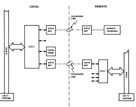
The DZQll is a Q-bus option. Its outline is shown in Figure 1-1. The DZQll is an asynchronous multiplexer that interfaces between a Q-bus processor and four asynchronous serial data communication lines. It can be used in many applications such as data concentration, real-time processing, and cluster controlling. The DZQll communications interfaces are compatible with RS-232-C (V.28) and RS-423-A (V. 1 O/X.26). There is enough modem control to permit dial-up ( auto-answer) operation with full-duplex modems *, such as the Bell models 103, 113, 212, or equivalent. Remote full-duplex working, as a control (master) station over private lines, is also possible for point-to-point or multipoint operation. Figure 1-2 shows some possible applications for the DZQ 11 in a Q-bus system.
All the DZQ 11 parameters can be easily controlled. These parameters are: • Baud rate
• Character length
• Number of stop bits for each line • Odd or even parity for each line • Transmitter receiver interrupts. Additional features include:
• Limited modem control • Zero receiver baud rate
• Break generation and detection • Silo buffering of received data • Line turnaround.
The DZQIl is program-compatible with the Q-bus DZVll and with the UNIBUS optionDZII-A. The only exception is the number of serial lines supported. The DZQ 11 does not support 20 rnA operation. Documents describing the DZQ 11 are:
• DZQll Asynchronous Multiplexer User's Guide - EK-DZQII-UG • DZQl1 Asynchronous Multiplexer Technical Manual- EK-DZQII-TM • Field Maintenance Printset - MP01795
• DZQll Maintenance Card - EK-DZQII-MC
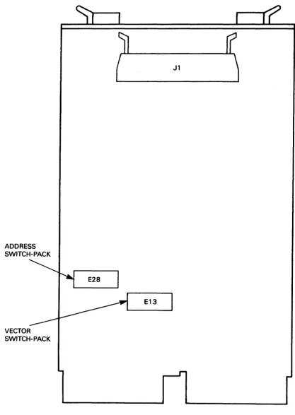
ADDRESS SWITCH-PACK
VECTOR SWITCH-PACK
J1
E28
E13
[image:6.615.100.518.71.658.2]R01789
1.2 PHYSICAL DESCRIPTION
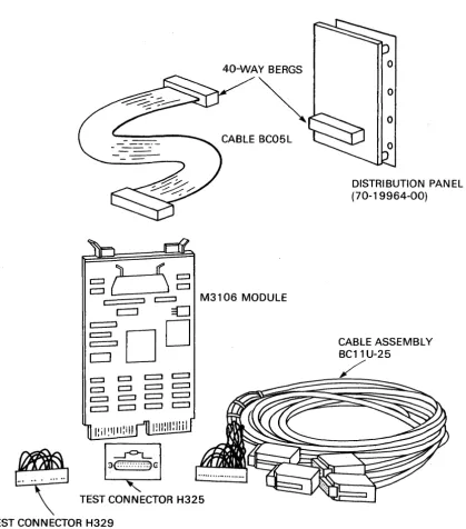
The DZQ 11 is made up of two components connected by a ribbon cable. The components are:
1. A single dual-height module, 21.6 X 13.2 cm(8.51 X 5.19 inches), called the M3106 module. All input and output connections are available on a Berg
*
header. This module includes all active circuitry as well as the line drivers and receivers.2. A distribution panel 6.7 X 8.5 cm(2.6 X 3.3 in) which contains four filtered D-type connectors and a Berg header. This header connects to the M31 06 by means of a 40-way ribbon connector.
NOTE
A 07272 Orant Continuity card may be needed. Refer to Section 2.3.2 for an explanation.
LOCAL REMOTE
DZ011
DATA SET
LOCAL TERM.
DATA SET
I
TELEPHONE LINEDATA
--c1t-
- SETI
I
I
I
I
__
?~_ ~:;A
I
TELEPHONEI
LINEFigure 1-2 DZQ11 System Applications
* Berg is a registered trademark of the Berg Corporation.
REMOTE TERMINAL
DZ011
[image:7.620.83.552.251.620.2]1.2.1 DZQII Configurations
The basic option supplied is the DZQII-M and is made up of the following:
1. Logic Module 2. User's Guide 3. Maintenance Card
M3I06
EK-DZQI1-UG EK-DZQII-MC H329
4. Turnaround test connector
The basic option (DZQ 11-M) can be supplied with one of five cabinet kits for installation into different systems. These are:
1. CK-DZQI1-DA (21-inch cable), example of use - PDP-ll/23S 2. CK-DZQII-DB (12-inch cable), example of use - Micro/PDP-II 3. CK-DZQII-DC (30-inch cable), example of use - PDP-l 1/23+ 4. CK-DZQII-DF (36-inch cable), example of use - PDP-ll/83 5. CK-DZQI1-D3 unshielded option (BCll U-25 cable).
The first four cabinet kits are almost identical except for the length of the flat ribbon cables, and the addition of an adapter plate in the CK-DZQI1-DC. They are made up of the following:
1. BC05L-xx cable (see NOTE) 2. H325 line-Ioopback connector
3. The distribution panel - 70-19964-00
4. Mounting bolts and washers for the distribution panel.
A system integrated DZQ11 option is a DZQII-DP.
NOTE
The distribution panels provide noise filtering and static discharge protection on the communi-cations lines. The -DC version has an adapter plate which allows the panel to be mounted in the PDP-I 1/23+.
BC05 L-xx cables are supplied in different lengths for each kit as previously specified.
40-WA Y BERGS
~
CABLE BC05L
~b~
c ::J c:::::::J M3106 MODULEc:::J
=D
~DD
I: i I ~ 'III: i "
la~GI
TEST CONNECTOR H325
TEST CONNECTOR H329
o
o
DISTRIBUTION PANEL (70-19964-00)
CABLE ASSEMBLY BC11 U-25
/
RD1790
[image:9.617.109.529.61.538.2]1.2.2 Interface Cables
The connections from the DZQ 11 use 25-pin male subminiature D-type connectors as specified for RS-232-C.
Circuit AA (CCITT* 101) Circuit AB (CCITT 102) Circuit BA (CCITT 103) Circuit BB (CCITT 104) Circuit CD (CCITT 108.2) Circuit CE (CCITT 125) Circuit CF (CCITT 109)
Pin 1 Pin 7 Pin 2 Pin 3 Pin 20 Pin 22 Pin 8
Protective Ground Signal Ground Transmitted Data Received Data Data Terminal Ready Ring Indicator
Carrier
NOTE
Signal ground and protective ground are connected together, through the chassis, by jumper WI on the 70-19964-00 distribution panel.
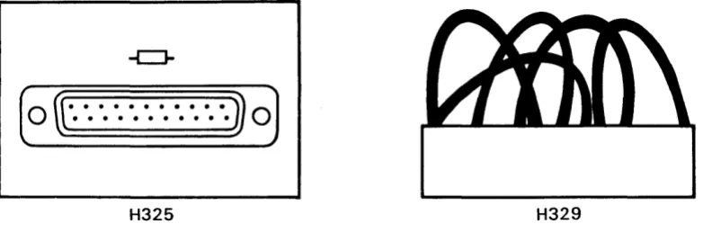
1.2.3 Test Connectors
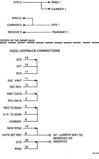
Figure 1-4 shows the two accessory test connectors, H329 and H325.
The H329 plugs into the module I/O connector and connects line 0 to line 1, and line 2 to line 3. The H325 plugs into an EIA connector on the distribution panel, or BC11 U-25 cable assembly, to loopback data and modem signals over a single line. The loopback connections are shown in Figure 1-5.
.
. .
.
. .
. .
. .
.
· · · .. 0
H325 H329
R01S5'
Figure 1-4 Test Connectors H325 and H329
[image:10.613.112.503.408.537.2]NOTE:
H329 STAGGERED TURNAROUND
TRANSMIT a ---~.~ RECEIVE 1
DTRa
---"""":~
RING 1 " - - - . CARRIER 1RING a :
CARRIER a "'~---'"---- DTR 1
RECEIVE a "'4~---TRANSMIT 1
LINE 2&3 ARE STAGGERED IN THE SAME WAY.
-H325 LOOPBACK CONNECTIONS
:::8
1 1 SEC XMIT - - - ,SECRCV
~
XMITDATA~
RCVDATA~
4REQTOSEND
9
CLR TO SENDCARRIER 8
14
NEW SYNC
-I
DATA SET ROY 6
20
DTR
J
22RING
0 Wl JUMPER MAY BE REMOVED OR
0 INSERTED
Figure 1-5 Loopback Connection
[image:11.613.189.518.126.655.2]1.3 SPECIFICATIONS
Environmental, electrical, and performance specifications for the DZQ 11 are listed in the following paragraphs.
1.3.1 Environmental Storage temperature
Operating temperature
Relative humidity 1.3.2 Electrical
Power consumption
Q-bus loading
1.3.3 Performance
o
degrees C to 66 degrees C (32 degrees F to 151 degrees F)5 degrees C to 60 degrees C (41 degrees F to 140 degrees F)
10% to 95% non-condensing
1.100 A at +5 V dc typical 0.236 A at
+
12 V dc typical Q-bus ac loadsQ-bus dc loads
1.5 ac loads 1.0 dc loads
The following paragraphs describe the DZQ 11 performance capabilities and restrictions.
1.3.3.1 Interfaces - The DZQl1 interfaces with the host computer bus and also with the four data communication lines.
1. System Bus Interface
The DZQ 11 module interfaces directly to a Q22 or other Q-bus via connectors A and B. The
module meets the DIGITAL Q-bus specification. 2. Serial Interfaces
The DZQ 11 serial interfaces comply with a subset ofEIAICCITT standards RS-232-C/V.24. The electrical characteristics are compatible with EIAICCITT standards RS-232-C/V.28 and RS-423/V.I0 (unbalanced interface).
1.3.3.2 Maximum Configurations - The DZQl1 multiplexer is assigned a device address in the floating address space. The floating address space starts at 7600108 and extends to 7637768. Maximum configuration of DZQ 11 s is not limited by floating address space, but is limited by the rules controlling a system configuration of average size.
As the DZQ 11 needs one backplane AB slot-pair, it is physically possible to mount • Two M3106 modules in a PDP-l1/23-S
• Three M3106 modules in a Micro/PDP-II • Four to five M3106 modules in a PDP-l1/23+
1.3.3.3 Throughput - Each DZQ 11 is capable of a throughput of 10 970 characters per second ( chars/ s). This rate is computed as follows.
(Bits/ s X number of lines X directions) divided by bits/char
(9 600 X 4 X 2)/7 equals 10 970 chars/ s, at 5 bits/char with one start and one stop bit and no parity. The full device throughput can only be maintained when a character service routine takes 100 microseconds or less.
The DZQ 11 has a maximum non-standard data rate of 19 800 baud. At this rate the throughput is 22 625 characters per second.
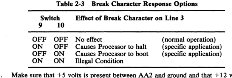
1.3.3.4 Receivers - The receivers perform serial-tc:rparallel conversion of 5-, 6-, 7-, or 8-level code with one start bit and at least one stop bit. The character length, number of stop bits, parity generation, and operating speed are programmable parameters for each line. Both the receiver and the transmitter of a corresponding line share the same operating speed, and the receiver line can be enabled or disabled. Each receiver is double buffered and has an acceptable input distortion of 43.75% on any bit. The sum of the character distortion must also not exceed 43.75 %. An exception to this is the stop bit. The stop bit can tolerate an error of 50%, that is, the receiver will accept a stop bit as short as one half of a bit period. Break detection is provided on each receiver via a register bit. In addition, the configuration of switchpack E 13-9 and E13-10 can cause the processor to boot or halt when a break is detected on line 3.
1.3.3.5 Transmitters - The transmitters provide parallel-tc:rserial conversion of 5-, 6-, 7- or 8-level code with or without parity. The parity sense, when selected, can be either odd or even. The stop code can be either 1 or 2 units except when 5-level code is selected. When 5-level code is selected, the stop code can be set to 1 or 1.5 units. The character length, number of stop units, parity generation and sense, and operating speed are programmable parameters for each line. The operating speed for the transmitter is common with the receiver. Breaks can be transmitted on any line. The maximum start-stop distortion for the output of a transmitter is less than 2.5% for an 8-bit character.
1.3.3.6 Baud-Rate Generator - The baud-rate generators are completely programmable. Each line has an independent generator which can select 1 of 16 baud rates. Speed tolerance for all rates is better than 0.3%. The baud rates are shown in Section 1.3.3.7.
1.3.3.7 Performance Summary - The following list shows the programmable features offered for each line.
Character length Number of stop bits
Parity Baud rates
Breaks
5-, 6-, 7-, or 8-level code
1 or 2 for 6-, 7-, or 8-level code. 1 or 1.5 for 5-level code
Odd, even, or none
50, 75, 110, 134.5, 150,300,600, 1 200, 1 800,2000,2400,3 600, 4800, 7 200, and 9 600 (and non-standard 19 800)
Can be generated and detected on each line
1.3.4 Interrupts
The following interrupts are available on the DZQ 11.
1.3.4.1 Receiver-Done Interrupt - The receiver-done interrupt occurs every time a character appears at the output of the receiver buffer register and the silo alarm is disabled. The receiver-done interrupt can be enabled or disabled from the bus.
1.3.4.2 Silo-Alarm Interrupt - The silo-alarm interrupt occurs after 16 entries have been made into the receive buffer register by the scanner. This interrupt disables the receiver-done interrupt, and is armed again when the receive buffer register has been read.
2.1 SCOPE
CHAPTER 2
INSTALLATION
This chapter contains the procedures for the unpacking, installation, and initial checkout of the DZQ 11 asynchronous multiplexer. It contains information on the following:
•
•
•
•
Device and vector address selection Recommended cables
Testing after installation
Floating address and vector assignment. 2.2 UNPACKING AND INSPECTION
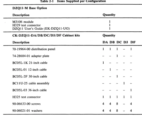
The DZQll is packed following normal commercial packing practices. To unpack, first remove all packing material and check the equipment against the shipping list. (Table 2-1 contains a list of supplied items per configuration.) Report any damage or shortages to the shipper immediately and inform the local DIGITAL office. Examine all parts and carefully examine the module for damage, loose components, and breaks in the etched paths.
CAUTION
The M3106 is supplied in a protective sleeve. Do not remove the sleeve until you are about to install the module. Protect the module from static during installation.
WARNING
Table 2-1 Items Supplied per Configuration
DZQII-M Base Option
Description Quantity
M3106 module 1
H329 test connector 1
DZQll User's Guide (EK-DZQII-UG) 1
CK-DZQII-DA/DB/DC/D3/DF Cabinet kits Quantity
Description DA DB DC D3 DF
70-19964-00 distribution panel 1 I I 1
74-28684-01 adapter plate 1
BC05L-IK 21-inch cable 1
BC05L-Ol 12-inch cable 1
BC05L-2F 30-inch cable 1
BCll U-25 cable assembly I
BC05L-03 36-inch cable 1
H325 test connector 1 1 1 I 1
90-06633-00 screws 4 4 8 4
90-06021-01 washers 4 4 8 4
2.3 INSTALLATION PROCEDURE
The following paragraphs describe the installation of the DZQ 11 option in a Q-bus system.
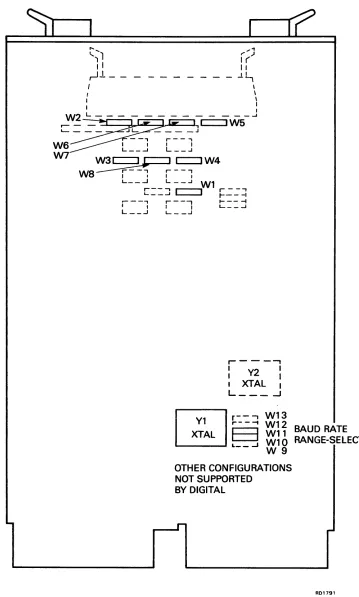
2.3.1 Modem Control Jumpers
[image:16.615.47.539.83.486.2]..
~~I
-I
r
.... 1
f' )
I (
II
- - - ...LL,
\,
\I ~
I I
W2 L - - - _ _ ...J
~.~-__ ~~ _~]c:::::JW5
- - , r - - " '
W6
L __
J
L __J
W7
W8~ :~W4
J I I I
L _ _ ..J L __ ..J Wl
C::J
c::=:J ~-=-=-::. - - - , , - - - , 1----1
I I I I L _ _ ...J
L __ .J L _ _ ..J
,---..,
I Y2 I I I
I XTAL I
L _ _ _ ...J
[]J
l~::::: ~~~
r=:::J BAUD RATE XTAL c:::::J Wll RANGE-SELECT
L _ _ ..J ~1~ OTHER CONFIGURATIONS NOT SUPPORTED
[image:17.612.127.486.71.668.2]BY DIGITAL
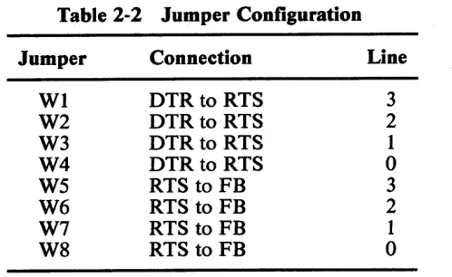
Figure 2-1 Jumper Location on M3106 Module ,..
Table 2-2 Jumper Configuration Jumper
WI W2 W3 W4 W5 W6 W7 W8
2.3.2 Module Installation
Connection DTR to RTS DTR to RTS DTR to RTS DTR to RTS RTS to FB RTS to FB RTS to FB RTS to FB
To install the M3106 module, perform the following.
NOTE
Line
3 2 1
o
3 2
1
o
This checkout procedure should be performed by trained maintenance personnel only.
CAUTION
Switch ofT power before inserting or removing modules.
The M3106 is a fine-line-etch PCB. Handle it carefully to avoid damaging the etch.
Take anti-static measures to protect the module.
1. The Q-bus Interrupt Acknowledge and the DMA Grant signals are daisy-chained through the AB slots of the Q-bus backplane. If a DZQ 11 is followed by a quad-size option in an AB/ AB (Q/Q) backplane, it may cause an AB slot-pair to be left vacant. In order to maintain the continuity of the daisy-chained signals, a G7272 Grant Continuity card should be installed in the vacant A slot.
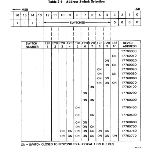
2. Refer to Section 2.4 for descriptions of the address assignments. Set the switches at E28 so that the module responds to its assigned address. When a switch is closed (ON), a binary 1 is encoded. When a switch is open (OFF), a binary 0 is encoded. The switch numbered 1 is connected to address bit 12, 2 is connected to address bit 11, and so on (Table 2-4).
3. The 10-position switch at E13 performs the vector selection. Switch position 7 is not used. Switch position 6 is connected to vector bit 3,5 is connected to vector bit 4, and so on. When a switch is closed (ON), binary 1 is encoded. When a switch is open (OFF), a binary 0 is encoded (Table 2-5).
4. Position 8 of the vector selection switch is a test switch which can disconnect the DZQ 11 oscillator from all circuitry. Make sure that this switch is in the ON position before installation.
[image:18.612.185.434.71.224.2]Table 2-3 Break Character Response Options Switch Effect of Break Character on Line 3
9 10
OFF OFF No effect
ON OFF Causes Processor to halt OFF ON Causes Processor to boot ON ON Illegal Condition
(normal operation) (specific application) (specific application)
6. Make sure that +5 volts is present between AA2 and ground and that + 12 volts is present between AD2 and ground. Measure at the nearest accessible point, if the backplane cannot be accessed.
7. Remove power and insert the module in an AB slot of the backplane.
8. Apply power and make sure that the +5 volts and +12 volts is present with the module installed.
CAUTION
Insert and remove modules slowly and carefully to prevent damage to the module components on the card guides, and to avoid changing switch selections in error.
"THIS SIDE UP"
M3106 MODULE
nnOD
0
~n~
n
00
OUDO
0
Du
DOnO
[image:19.617.102.491.80.211.2]nnnn
Olln
00
Figure 2-2 DZQll Installation (BCll U-25)
[image:19.617.104.532.404.609.2]Table 2-4 Address Switch Selection
-+---- MSB LSB
16 15 .14 13
121111101
91
a \
71
61
51
4 3 2 1 01 1 1 1 SWITCHES
.
0 0 0 0SWITCH E28 E28 E28 E28 E28 E28 E28 E28 E28 E28 DEVICE NUMBER 1 2 3 4 5 6 7 8 9 10 ADDRESS
17760000 ON 17760010 ON 17760020 ON ON 17760030
ON 17760040
ON ON 17760050 ON ON 17760060 ON ON ON 17760070
ON 17760100
ON 17760200
ON ON 17760300
ON 17760400
ON ON 17760500
ON ON 17760600
ON ON ON 17760700
ON ON ON ON ON ON ON 17763760 ON ON ON ON ON ON ON ON 17763770
ON
=
SWITCH CLOSED TO RESPOND TO A LOGICAL 1 ON THE BUS [image:20.617.51.517.76.620.2]MSB
15 14 13 12 0 0 0
REFER TO
SECTION 2.3.2
FOR SETTING
0
OF E13 - 7 TO 10
Table 2-5 Vector Switch Selection
11 10 9 8
I
7I
6I
5I
4I
0 0 0 SWITCHES
SWITCH E13 E13 E13 E13 E13
NUMBER 1 2 3 4 5
ON ON ON ON
ON ON ON
ON ON ON
ON ON ON ON ON ON ON ON ON ON ON ON ON ON ON
ON ON
ON ON ON ON ON
ON ON ON ON ON ON ON ON ON ON
LSB
3 2 1 0
-
1/0 0 0E13 VECTOR
6 ADDRESS
300
ON 310
320
ON 330
340
ON 350
360
ON 370
400 500 600 700
760
ON 770
ON
=
SWITCH CLOSED TO PRODUCE A LOGICAL 1 ON THE BUS [image:21.617.89.510.84.499.2]Q-BUS BACKPLAN E GATE ARRAY
70-19964-00
DISTRIBUTION PANEL
[image:22.613.67.545.70.546.2]RED LINE TO "A"
Figure 2-3 DZQll Installation (70-19964-00) 2.3.3 Testing DZQlls in PDP-II Systems
CHANNELS
o
2
3
R018S2
The following diagnostics are available to test DZQl1s installed in PDP-II systems. DZITA and DVDZD are only used when a link between two processors is to be tested.
CVDZA CVDZB CVDZC CXDZB DZITA DvnZD
DZVl1/DZQll Logic Test - Part 1 DZVll/DZQl1 Logic Test - Part 2 DZVll/DZQl1 Cable/Echo Test DECX/ll Module
Test the option as follows.
1. Run diagnostics CVDZA and CVDZB in internal mode, to verify operation. Refer to the listing for more help. Run at least three passes without error.
2. Insert the H329 test connector in Jl with the letter side facing up. Jl is the cable connector at the top of the M3106 module.
Run CVDZA and CVDZB in the staggered mode, to verify module operation. Refer to the diagnostic listing for the correct procedure. Run at least three passes without error.
3. If the unshielded cab-kit (D3) version is used, replace the H329 test connector with the Berg end of the BCII U cable assembly. Follow the 'This side up' instruction on the assembly. Refer to Figure 2-2 for assembly and interconnection instructions.
4. If the cab-kit versions CK-DZQ 11-DA, -DB or -DF are used, feed the cable through the rear of the cabinet and connect the Berg plug to the distribution panel. Mount the distribution panel in the opening at the rear of the cabinet
The -DC version is provided with an adapter plate to fit the large opening in a PDP-I 1/23+. Mount the adapter plate on the distribution panel, with four of the eight screws provided. Mount the distribution panel as described above.
5. Connect the H325 test connector on the first line and run diagnostic CVDZC. Select the cable-test part of the diagnostic. Three passes are needed without error. Repeat this step for each line.
6. Run the DECX/Il system exerciser to verify the absence of Q-bus interference with other system devices.
7. The DZQ II is now ready for connection to external equipment. If the connection is to a local terminal through either of the two options (BCII U-25 or 70-19964-00), a null modem cable assembly must be used. Use the BC22A, BC22D, or BC03P null modem cables for connection between the option and the terminal. The H312-A null modem unit may also be used in place of the null modem cables.
Connections between the option and a modem should be made using a BC22E or BC05 D cable.
All of the cables referred to, with the exception of the BCII U-25, must be ordered separately as they are not components of a DZQ II option.
2.3.4 Testing in Micro V AX Systems
The following diagnostic tests are available for testing DZQ 11 s in Micro V AX systems.
DZVll/DZQll Test EHXDZ
EHKMV Macroverify - MicroV AX System Test
Macroverify is a standalone diagnostic which contains a DZVll/DZQll test module.
Refer to the appropriate diagnostic listing, or to Chapters 11 and 14 of the Micro V AX Owner's Guide, for details of how to run EHXDZ and EHKMV.
Test the option as follows.
1. Boot from the Micro V AX system tests diskette (number 2 of2). Attach and select the DZQ 11 that is to be tested.
2. Run EHXDZ for three error-free passes of the internal (default) test.
3. Install the H329 staggered loopback connector on the M31 06 module. Run EHXDZ for three error-free passes of the staggered test.
4. Remove the H329. Install the BC05L cable and the distribution panel.
5. If the operation of a terminal link is to be tested, connect the terminal line to the distribution panel. Run the EHXDZ echo test on that line until the link· is proven. Depending on the terminal, a null-modem may be needed for this test. Exit echo test 1?y A Z (CTRL/Z).
6. Remove all external cables and connectors from the distribution panel. Boot the CPU tests diskette (number 1 of 2). The Macroverify diagnostic will run automatically when the boot process is complete. When the test completes, the status of all options will be displayed.
7. If no device has a TEST FAILED status, the DZQ 11 is now ready for connection to external equipment. If the connection is to a local terminal, a null modem cable assembly must be used. Use the BC22A, BC22D, or BC03P null modem cables for connection between the option and the terminal. The H312-A null modem unit may also be used in place of the null modem cables.
Connections between the option and a modem should be made using a BC22E or BC05 D cable.
All of the referenced cables must be ordered separately as they are not components of a DZQ II option.
2.4 DEVICE ADDRESS ASSIGNMENTS
On UNIBUS and Q-bus systems, a range of addresses (xxx600 1 08 to xxx63 77 68) in the top 4 K words is assigned as floating address space (xxx means all top address bits
=
1).The first part of the list of options (sufficient to include the DZQ 11) which can be assigned floating device addresses is given in Table 2-6. 'Rank' gives the sequence of address assignment for both Q-bus and UNIBUS options.
Table 2-6 Floating Address Assignments
Rank Device Size
(decimal)
1 DJ11 4 words
2 DH11 8 words
3 DQ11 4 words
4 DUll, DUV11* 4 words
5 DUP11 4 words
6 LK11A 4 words
7 DMC11/DMR11 4 words
8 DZ11, DZS11,
DZQ11*/DZV11*
DZ32 4 words
*
Q-bus deviceFor example, the address assignment sequences could be:
UNIBUS DJ11 DH11 DQ11 DUll DUP11 LK11A DMC11 DZ11
Q-bus
No Q-bus equivalent of DJ11 No Q-bus equivalent of DH11 No Q-bus equivalent of DQ 11 DUV11
No Q-bus equivalent of DUP11 No Q-bus equivalent of LKII A No Q-bus equivalent of DMCII DZQ 11 an~ so on.
Modulus (octal)
10
20
10
10
10
10
10
10
Devices of the same type are given sequential addresses, therefore all DUV11 s in a system will have lower addresses than DZQ 11 s or DZV11 s.
For the purpose of address assignment, DZQ 11 s and DZVll s are considered as devices of the same type.
[image:25.613.60.552.94.345.2]The assignment rules are as follows.
1. Addresses, starting at xxx60010, are assigned according to the sequence of Table 2-6 2. Option and gap addresses are assigned according to the octal modulus as follows.
a. Devices with an octal modulus of 10 are assigned an address on a 108 boundary (the three lowest-order address bits = 0)
b. Devices with an octal modulus of 20 are assigned an address on a 208 boundary (the four lowest-order address bits = 0)
3. Address space equal to the device's modulus must be allowed for each device which is connected to the bus
4. A one-word gap, assigned according to rule 2, must be allowed after the last device of each type. This gap could be bigger when rule 2 is applied to the following rank
5. A one-word gap, assigned according to rule 2, must be allowed for each unused rank on the list if a device with a higher address is used. This gap could be bigger when rule 2 is applied to the following rank
Two examples of address assignment follow. Table 2-7 shows addresses for a system with one DUV11 and one DZQ 11. Table 2-8 shows addresses for a system with no DUV11 and two DZQ 11 s. Note that where there is no Q-bus device at a specific rank, the UNIBUS device parameters must be used to assign the gap. Vector assignments (see Section 2.5) are also shown in these tables.
Table 2-7 is supported by a description of how to apply the assignment rules. Table 2-7 One DUVII and One DZQl1
Rank Address Designation Vector
1 xxx60010 DJ11 gap
2 xxx60020 DH11 gap
3 xxx60030 DQ11 gap
4 xxx60040 DUVII 300
xxx60050 DUV11 gap
5 xxx60060 DUP11 gap
6 xxx60070 LK11A gap
7 xxx60100 DMC11 gap
8 xxx60110 DZQl1 310
xxx60120 DZQl1 gap
The first floating address is 760010. As a DJl1 has a modulus of 108, its gap can be assigned to 760010. The next available location becomes 760012.
[image:26.620.84.543.98.348.2] [image:26.620.67.548.420.595.2]TheDUV11 has amodulusof108. It cannot be assigned to 760032. It is therefore assigned to 760040. As the size of DUV11 is four words, the next available address is 760050.
There is no second D UV11, so a gap must be left to indicate that there are no more D UV11 s. As 760050 is on a lOs boundary. The DUVl1 gap can be assigned to this. The next available address is 760052. And so on.
Rank 1 2 3 4 5 6 7 8 8 Address xxx60010 xxx60020 xxx60030 xxx60040 xxx60050 xxx60060 xxx60070 xxx60100 xxx60110 xxx60120
Table 2-8 Two DZQlls Designation
DJ11 gap DHll gap DQ11 gap DUV11 gap DUP11 gap LK11Agap DMC11 gap 1st DZQ11 2nd DZQll DZQl1 gap
2.5 INTERRUPT VECTOR ADDRESS ASSIGNMENTS
Vector
300 310
Addresses between 300s and 774s are designated as the floating vector space. These addresses are assigned in sequence as in Table 2-9.
Each device needs two 16-bit locations for each vector. For example, a device with one receive and one transmit vector needs four words of vector space.
The vector assignment rules are as follows.
1. Each device occupies vector address space equal to 'Size' words. For example, the DLV11-J occupies 16 words of vector space. If its vector was 3008 the next available vector would be 3408.
2. There are no gaps, except those needed to align an octal modulus.
The vector addresses shown in Tables 2-7 and 2-8 are assigned according to these rules. Table 2-9 First Part of Q-bus Vector Address Assignments List Device DLVI1-J DLVll,DLV11-F DRVI1-B DRVl1 DLVI1-E VSV11 KWV11 DUVl1 DZVl1/DZQll
Size Modulus
(decimal) (octal)
16 10
4 10
4 10
4 10
4 10
8 10
4 10
4 10
[image:27.612.67.556.560.725.2]3.1 SCOPE
CHAPTER 3
DEVICE REGISTERS
This chapter describes the format and bit function of each register in the DZQ 11. 3.2 DEVICE REGISTERS
The DZQll contains six addressable registers. Figure 3-1 shows the bit assignments of these registers and Table 3-1 lists the registers and related DZQ 11 addresses.
Table 3-1 DZQll Register Address Assignments Register Name
Control and Status Reg. Receiver Buffer
Line Parameter Register Transmitter Control Reg. Modem Status Register Transmit Data Register
Mnemonic
CSR RBUF LPR TCR MSR TDR
Address
76XXXO 76XXX2 76XXX2 76XXX4 76XXX6 76XXX6
Program Capability Read/Write Read Only Write Only Read/Write Read Only Write Only
xxx
=
Selected in agreement with the floating device address system.3.2.1 Control and Status Register
[image:28.613.62.549.303.422.2](j,)
I
N
CONTROL & STATUS
(CSR) RECEIVER BUFFER (RBUF) LINE PARAMETER (LPR) TRANSMIT CONTROL (TCR) MODEM STATUS (MSR) TRANSMIT DATA (TOR) MSB 15 RO
1
-TROY
RO
~---DATA VALID
~
~o Q~
.:5
~
o~~~
.:>
~o
t$
~
~t:O,
~,:;~
14 13
RW RO
~--
~---TIE SA
RO RO
---
---.
OVRN FRAM ERR ERR
~
~bi
~'"~
s-~
l#
~o "kQ~""
.:> ~t:O,
~~bi-
~ ,,~~ ~
f~
,
~~
.::>t"j12 11 10
RW t
-i
if
O~SAE ~ ~~
"
.::>RO
~----~
,
PAR
ERR
,s;
.::>""WO WO WO
----
RX SPEED SPEEDENAB CODE CODE D C
RW
~~--VI
1-~o Q DTR
4'
DTR~ 3 2 RO RO
--I
~------~4'
~ CO CO 3 2
WO WO
trI
~-----~t:O BRK BRK 3 2
09
RO
1
-TLiNE B RO
----
RX LINE B WO SPEED CODE B~I!..W __ DTR 1 RO ~-
--CO 1 WO ---BRK 1 BYTES HIGH LOW 08 07RO RO
--TLiNE IRDONE A
RO RO
1 - - - -
---RX
LINE RBUF A 07
WO WO
---SPEED ODD CODE PAR
A
!!,W __
~
DTR ~".J
0 .:>
RO
,
~---~~
CO .:>
0
WO WO
-
---BRK TBUF 0 7
06 flW __ RIE RO RBUF 06 WO
---
PAR ENAB,
~~ o~.:>
~
~~.:>
WO
1
-TBUF 6
Figure 3-1 Register Bit Assignment
LSB
05 04 03 02 01 00
RW RW RW
---
1-I~
~ Q~
~Q1;1
MSE CLR MAINT ~
~ ~
"
.:5 ~RO - - - -RO
---
RO RO RO RO1 - - - -
---RBUF ---RBUF RBUF RBUF RBUF RBUF
05 04 03 02 01 DO
WO WO WO WO WO
- - - -
----?
~------STOP CHAR CHAR ~o
t$
CODE LGTH LGTH
~""
LINE LINEB A B A
~
l'
~~-- _RlY_ t-R!l_ t-R~ __o~
~"" .;:, LINE LINE LINE LINE
~t:O ENAB ENAB
ENAB ENAB
3 2 1 0
?
;J
RO RO RO RO~---
---
I- - - -----~,:; ~
$
.:> ~t:O RI3 RI2 RI1 RIO
WO WO WO WO WO WO
--- --- foo----
1 - - - ---
1 -TBUF -TBUF TBUF TBUF TBUF TBUF5 4 3 2 1 0
[image:29.793.67.713.105.491.2]Bit <02:00> <03>
<04>
<05>
<06>
<07>
<09:08>
<11:10>
Title Not used Maintenance (MAINT)
Master Clear (CLR)
Master Scan Enable (MSE)
Receiver Interrupt Enable (RIE)
Receiver Done (RDONE)
Transmitter Line Number (TLINE B and TLINE A) Not used
Table 3-2 CSR Bit Assignments Function
This is a READ/WRITE bit. When set it loops the serial output connections of the transmitter to the corresponding serial input connections of the receiver at the UART. (Used for loopback test only.)
When written to aI, this bit generates 'initialize' within the DZQ 11. A read-back of the CSR with this bit set indicates initialize in progress within the device. This bit is self-clearing. All registers, silos, and UARTs are cleared with the following exceptions: 1. Only bit 15 of the receiver buffer register (Data Valid) is
cleared; the other bits
«
14:00» are not.2. The high byte of the transmitter control register is not cleared by Master Clear.
3. The modem status register is not cleared by Master Clear. This read/write bit must be set to permit the receiver and transmitter control sections to start scanning. When cleared, Transmitter Ready (CSR<15» is inhibited from setting, and the received character buffers (silos) are cleared.
This bit permits the generation of an interrupt, when CSR<07> or CSR<13> is set. This bit is read/write.
This is a read-only bit that is set when a character appears at the output of the first-in/first-out (FIFO) buffer. For the DZQll to run in the interrupt-per-character mode, CSR<06> must be set and CSR<12> must be cleared. With CSR<06> and CSR<12> cleared, character-flag mode is indicated. Receiver Done clears when the receiver buffer register (RBUF) is read or when Master Scan Enable (CSR<05» is cleared. If the FIFO buffer contains an additional character, the Receiver Done flag stays clear for up to 1 microsecond, while that character bubbles through to the bottom of the FIFO.
[image:30.615.58.564.80.740.2]Bit <12>
<13>
<14>
<15>
Title Silo Alarm Enable (SAE)
Silo Alarm (SA)
Transmitter Interrupt Enable (TIE) Transmitter Ready (TRDY)
3.2.2 Receiver ButTer
Table 3-2 CSR Bit Assignments (Cont) Function
This is a read/write bit. When set, it enables the silo-alarm and prevents RDONE (bit <07» from causing interrupts. If the receiver interrupt enable bit (bit <06> ) is set, SAE enables the silo-alarm (bit < 13> ) to generate an interrupt after 16 silo entries. If silo-alarm is not set, then SAE may be used as a flag to indicate that 16 or more characters are in the silo.
This is a read-only bit set by the hardware after 16 characters have been entered into the FIFO buffer. Silo Alarm is held cleared when Silo Alarm Enable (CSR < 12» is cleared. This bit is cleared by a read to the receiver buffer register and does not set until 16 additional characters are entered into the buffer. If Receiver Interrupt Enable (CSR<06» is set, the occurrence of Silo Alarm generates a receiver interrupt request. Flag mode operation of the Silo Alarm bit is permitted with CSR<06> cleared.
This is a read/write bit which must be set for Transmitter Ready to generate an interrupt.
This read-only bit is set by the hardware when the transmitter scanner stops on a line whose transmit buffer may be loaded with another character and whose related TCR bit is set. The transmitter line number, specified in CSR<09:08>, is only valid when Trans-mitter Ready is set. TransTrans-mitter Ready is cleared by any of the following conditions:
1. When Master Scan Enable is cleared.
2. When the related TCR bit is cleared for the line number pointed to in CSR <09:08>
If additional transmit lines need service, Transmitter Ready appears again within 1.4 microseconds of the completion of the 'transmit data register load' instruction. When Transmitter Ready occurs with Transmitter Interrupt Enable set, a transmitter interrupt request is generated.
Bit <07:00>
<09:08>
<11:10>
<12>
<13>
<14>
<15>
Table 3-3 RBUF Bit Assignments
Title Function
Received These bits contain the received character, right justified. the least-Character significant bit is bit <00>. For short characters, bits that are not (RBUF 0<7:0» used are logic low. The parity bit is not shown.
Received Line Number (RX LINE B and RX LINE A)
Not used
Parity Error (PAR ERR)
Framing Error (FRAMERR)
Overrun Error (OVRN ERR)
Data Valid (DATA VALID)
These bits contain the line number on which the Received Character was received. Bit <08> is the least significant.
This bit is set if the sense of the parity of the received character does not agree with the parity defined for that line.
This bit is set if the received character did not have a stop bit present at the correct time. This bit is usually interpreted as indicating that a break has been received.
This bit becomes set when a received character is overwritten in the UART buffer (by a following character), before it has been transferred by the scanner to the FIFO.
This bit, when set, indicates that the data in bits < 14:00> is valid. This bit permits the use of a character-handling program which again and again takes characters from the FIFO buffer until there are no more available. This is done by reading this register and checking bit < 15 > until the program gets a word for which bit < 15> is zero.
3.2.3 Line Parameter Register
The line parameter register (LPR) controls the operating parameters related to each line in the DZQ 11. The LPR must be addressed with a word address and is a write-only register. The line parameters for all lines must be loaded again following an occurrence of either BINIT or device Master Clear. Table 3-4 lists bit assignments.
Bit <01:00>
<02>
Title
Parameter Line Number
(LINE Band LINE A)
Not used
Table 3-4 LPR Bit Assignments Function
These bits specify the line number for which the parameter information (bits < 12:3» is to apply. Bit <00> is the least-significant bit.
[image:32.612.64.542.72.463.2]Bit <04:03>
<05>
<06>
<07>
<11:08>
Table 3-4 LPR Bit Assignments (Cont) Title
Character Length
(CHARLGTH
B and CHAR LGTHA)
Stop Code (STOP CODE) Parity Enable (PAR ENAB)
Odd Parity (ODD PAR)
Speed code (SPEED CODE D to SPEED CODE A)
Function
These bits are set to receive and transmit characters of the length (except parity) shown below.
Bit 04 Bit 03
0 0 5-bit
0 1 6-bit
1 0 7-bit
1 1 8-bit
This bit sets the stop code length; 0
=
1 unit stop, 1=
2 unit stop ( or 1.5 unit stop if a 5-level code is used).If this bit is set, characters transmitted on the line have an appropriate parity bit added, and characters received on the line have their parity checked.
If this bit is set, characters of odd parity are generated on the line and incoming characters are expected to have odd parity. If this bit is not set, but bit <06> is set, characters of even parity are generated on the line, and incoming characters are expected to have even parity. If bit <06> is not set, then the setting of this bit will not have any effect. The state of these bits determines the operating speed for the transmitter and receiver of the selected line.
11 10
09
08 Baud Rate0 0 0 0 50
0 0 0 1 75
0 0 1 0 110
0 0 1 1 134.5
0 1 0 0 150
0 1 0 1 300
0 1 1 0 600
0 1 1 1 1200
1 0 0 0 1800
1 0 0 0 2000
1 0 1 0 2400
1 0 1 1 3600
1 1 0 0 4800
1 1 0 1 7200
I 1 1 0 9600
1 1 1 1 19800
*
[image:33.612.54.551.66.679.2]Bit <12>
<15:13>
Table 3-4 LPR Bit Assignments (Cont)
Title Function
,
Receiver Enabled (RXENAB)
This bit must be set before the UART receiver logic can assemble characters from the serial input line. This bit is cleared following a BINIT or device Master Clear.
Not used
NOTE
The M3106 module can be modified by jumpers W9 to W13, so that code IIII selects baud rates other than 19 800. This modification is not supported by DIGITAL.
3.2.4 Transmitter Control Register
The transmitter control register (TCR) is a byte- and word-addressable register. The low byte of the TCR contains the transmitter control bits, and must be set to start transmission on a line. Each TCR bit position is related to aline number. For example, J'CR<OO> is related to line 00, bit <01> to line 01, and soon. Setting a TCR bit causes the transmitter scanner clock to stop if the UART for this line has a 'transmit buffer empty' condition. An interrupt is then generated if Transmitter Interrupt Enable is set. The scanner clock restarts when either the transmit data register (TDR) is loaded with a character or the TCR bit is cleared for the line on which the clock has stopped. TCR bits must only be cleared when the scanner is not running, (that is, Transmitter Ready is set or Master Scan Enable is cleared).
The line enable bits are represented in TCR<03:00>. These bits are read/write and are cleared by BINIT or device Master Clear. Bits <07:04> are not used, and are read as zero.
The high byte of the TCR register contains the modem control signal that can be written, data terminal ready (DTR). The bits are defined as follows:
Bit <08> <09> <10> <11> <15:12>
Name
DTRLine 00 DTR Line 01 DTRLine 02 DTRLine 03
Not used; read as zero
3.2.5 Modem Status Register
The modem status register (MSR) is a 16-bit read-only register. A read to this register gives the status of the modem control signals that can be read, Ring and Carrier. The ON condition of a modem control signal is interpreted as a logical one. Bits <07 :04> and < 15: 12> are not used and are read as a zero. The other bits are defined as follows:
Bit Name Bit Name
<00> Ring Line 00 <08> Carrier Line 00 <01> Ring Line 01 <09> Carrier Line 01 <02> Ring Line 02 <10> Carrier Line 02 <03> Ring Line 03 <11> Carrier Line 03
<07:04> Not used; read as <15:12> Not used; read as zero. zero
3.2.6 Transmit Data Register
The transmit data register (TDR) is a byte- and word-addressable, write-only register. Characters for transmission are loaded into the low byte. TDR<OO> is the least-significant bit Loading of a character should occur only when Transmitter Ready (CSR<15» is set The character that is loaded into this register is routed to the line defmed in CSR<09:08>. The high byte of the TDR is defined as the break control register.
4.1 SCOPE
CHAPTER 4
PROGRAMM1NG
This chapter contains information for programming the DZQ 11 in the most efficient way. To do so, the programming controls must be completely understood. The following paragraphs discuss the DZQ 11 from the programming point of view and describe recommended programming methods.
4.2 PROGRAMMING FEATURES
The DZQll has some programming features that allow control of baud rate, character length, stop bits, parity, and interrupts. This section discusses the application of these controls to get the wanted operating parameters.
4.2.1 Interrupts
The Receiver Interrupt Enable (RIE) and Silo Alarm Enable (SAE) bits in the CSR control the way that the DZQ 11 receiver interrupts the processor.
IfRIE and SAE are both clear, the DZQ 11 never interrupts the processor. In this event, the program must regularly check that the data is available in the silo, and empty the silo when data is present. If the program operates from a clock, it should check for characters in the silo at least as often as the time it takes for the silo to fill, allowing a safety element to cover processor-response delays and time to empty the silo. The Receiver Done (RDONE) bit in the CSR is set when a character is available in the silo. The program can regularly check this bit with a test byte or bit test instruction. When RDONE is set, the program should empty the silo.
IfRIE and SAE are both set, the DZQ 11 interrupts the processor to the DZQ 11 receiver vector when the Silo Alarm (SA) bit in the CSR is set. The SA bit is set when 16 characters have been placed in the silo after the last time the program has accessed the RBUF. Accessing the RBUF clears the SA bit and the related counter. The program should follow the procedure described in Section 4.2.2 to empty the silo completely in response to a Silo Alarm interrupt. This makes sure that any characters placed in the silo while it is being emptied are processed by the program.
NOTE
If the program processes only 16 entries in response to each Silo Alarm interrupt, characters coming in while interrupts are being processed build up without being counted by the Silo Alarm circuit. The silo may in the end overflow without the alarm being issued.
If the Silo Alarm interrupt is used, the program will not be interrupted when fewer than 16 characters are received. In order to respond to short messages during periods of medium activity, the program should regularly empty the silo. The scanning period depends on the wanted response time to received characters. While the program is emptying the silo, it should make sure that DZQ 11 receiver interrupts are inhibited. This should be done by raising the processor priority. The Silo Alarm interrupt feature can greatly decrease the processor overhead that would be needed by the DZQ 11 receiver. This is done by removing the need to enter and exit an interrupt service routine each time a character is received.
The Transmitter Interrupt Enable (TIE) bit controls transmitter interrupts to the processor. If enabled, the DZQ 11 interrupts the processor at the DZQ 11 transmitter interrupt vector when the Transmitter Ready (TRDY) bit in the CSR is set. This indicates that the DZQll is ready to accept a character to be transmitted.
Each DZQ 11 needs two interrupt vectors, one for the transmitter section and one for the receiver section. If simultaneous interrupt requests are generated from each section, the receiver section would have priority in placing its vector on the Q-bus. A receiver interrupt to address XXO is generated from having either a Receiver Done (CSR<07» or Silo Alarm (CSR<13» occurrence. A transmitter interrupt to address XX4 is generated by Transmitter Ready (CSR< 15». An additional prerequisite for generating interrupts is that the individual interrupt enable bits are set. The recommended method for clearing interrupt enable bits is first to raise the processor status word to level 4; next, to clear these interrupt enable bits; and then lower the processor status word to zero. Using this method prevents false interrupts from being generated.
4.2.2 Emptying the Silo
4.2.3 Transmitting a Character
The program controls the DZQ 11 transmitter through four registers on the Q-bus: the control and status register (CSR), the line parameter register (LPR), the transmit control register (TCR), and the transmit data register (TOR).
Following DZQ 11 initialization, the program must use the LPR to specify the speed and character format for each line to be used and must set the Master Scan Enable (MSE) bit in the CSR. The program should set the TIE bit in the CSR if it wants the DZQ 11 transmitter to interrupt the processor.
The TCR is used to enable and disable transmission on each line. One bit in this register is related to each line. The program can set and clear bits by using move, move byte, bit set, bit set byte, bit clear, and bit clear byte instructions. (If word instructions are used, the Line Enable bits and the DTR bits are accessed together.)
The DZQ 11 transmitter is controlled by a scanner which is continuously looking for an enabled line (Line Enable bit set) which has an empty transmitter buffer. When the scanner finds such a line, it loads the number of the line into the 2-bit transmit line number (TLINE) field of the CSR and sets the TROY bit, interrupting the processor if the TIE bit is set. The program can clear the TROY bit by moving a character for the indicated line into the TBUF or by clearing the line enable bit. Clearing the TROY bit allows the scanner to continue its search for lines needing service.
To start transmission on an idle line, the program should set the TCR bit for that line and wait for the scanner to request service on the line, as indicated by the scanner loading the number of the line into TLINE and setting TROY. The program should then load the character to be transmitted into the TBUF by using a move byte instruction. If the interrupts are to be used, a useful way of starting up a line is to set the TCR bit in the main program and let the normal transmitter interrupt routine load the character into the TBUF.
NOTE
The scanner may find a different line needing service before it finds the line being started up. This occurs if other lines request service before the scanner can find the Jine being started. The program must always cheek the TLINE field of the CSR when responding to TRDY, to make sure that it loads characters for the correct line. Assuming the program services lines as requested by the scanner, the scanner in the end finds the line being started. If more than one line needs service, the scanner requests service in priority order as determined by Jine number. Line 3 has the highest priority and Jine 0 the lowest.
To continue transmission on a line, the program should load the next character to be transmitted into the TBUF each time the scanner requests service for the line as indicated by TLINE and TROY. Because the transmitters are double buffered, a high-priority line may request two consecutive loads.
The normal rest condition of the transmitted data connection for any line is the one state. The Break (BRK) bits are used to apply a continuous zero signal to the line. One bit in the TDR is related to each line. The line stays in this condition as long as the bit stays set. The program should use a move byte instruction to access the BRK bits.
If the program continues to load characters for a line after setting the BRK bit, transmitter operation appears normal to the program regardless of the fact that no characters can be transmitted while the line is in the continuous zer<rsending state. The program may use this facility for sending correctly timed zero signals by setting the BRK bit and using transmit ready interrupts as a timer. The program must also make sure that the line returns to the one state at the end of the zer<rsending period before transmitting any additional data characters.
The following procedure does this. When the scanner requests service the first time after the program has loaded the last data character, because the lines are double buffered, the last data character has only started transmission. The program should therefore load an all zero character, and wait for the next service request while the last character is transmitted. When the scanner requests service the second time, the program should set the BRK bit for the line, and the zero character is overwritten. At the end of the zer<r sending period, the program should load an all zero character to be transmitted. When the scanner requests service, indicating this character has started transmission, the program should clear the BRK bit and load the next data character.
4.2.4 Data Set Control
The program may sense the state of the Carrier and Ring Indicator signals for each modem and may control the state of the Data Terminal Ready signal to each modem. The program uses two registers to access the DZQ 11 modem control logic. There are no hardware interlocks between the modem control logic and the receiver and transmitter logic. Any wanted sequence should be done under program control.
The Data Terminal Ready (DTR) bits in the TCR are read/write bits. Setting or clearing a bit in this register turns the appropriate DTR signal on or off. The program may access this register with word or byte instructions. (If word instructions are used, the DTR and Line Enable bits are accessed together.) The DTR bits are cleared by the INIT signal on the Q-bus but are not cleared if the program clears the DZQ 11 by setting the CLR bit of the CSR