United
States Patent
[19]Lipcon
[54] TRANSCEIVER FOR LOCAL NETWORK USING CARRIER-SENSE MULTIPLE ACCESS/COLLISION DETECI'ION [75] Inventor: Jesse B. Lipcon, Harvard, Mass. [73] Assignee: Digital Equipment Corporation,
Maynard, Mass. [21] Appl. No.: 267,394 [22] Filed: May 26, 1981
[51] Int. 0.3 •••••••••••••••••••••••••• H04B 1/00; H04B 1/40 [52] U.S. Cl. ... 455/58; 455/78; 340/825.5 [58] Field of Search ... 455/58, 73, 78; 370/85.93; 375/36; 340/825.5, 825.51; 364/900 MS File [56] References Cited
U.S. PATENT DOCUMENTS
3,048,764 8/1962 Murphy ... 455/78 3,465,252 9/1969 McLean et al. ... 455/78 3,742,450 6/1973 Weller ... 375/36 4,063,220 12/1977 Metcalfe ... 340/825.5
40
LOW-PASS FILTER
52
62
44
BAND-[11]
[45]
Primary Examiner-Jin F. Ng
4,384,363
May 17,
1983
Attorney, Agent, or Firm-Cesari and McKenna
[57] ABSTRACI'
A transceiver for a carrier-sense multiple access com-munications network using collision detection for con-trolling access to the network, and utilizing industry standard emitter-coupled logic (ECL) circuits in its receiver and transmitter. The transmitter output stage is an ECL current source. To prevent saturation of the transmitter output in the event of a collision, due to the voltage swing exceeding the compliance limit of the ECL current source, with a resulting failure of the collision detection mechanism, the power supply for the transmitter output stage supplies voltage in a first range of about -5 to -10 volts, while the power supply for the receiver input and collision detection circuits supplies voltage in a second, contiguous range of zero to about - 5 volts. This permits the transmitter output to swing about 6-7 volts without exceeding the compli-ance limit of the current source, so that the collision is detectable by the collision detection circuits.
1 Claim, 10 Drawing Figures
10 MHz OSCILLATOR
56
58
48
12A.---_~
14
BUFFER
r - - - -
I28
- - - . ,
I
26
25
II
I·
I
'
I
I
I I
I
I
L ____ -;0--- ___
J
16
32
CABLE
DRIVER
enable
- - -
-
-
- --
- - -
-
- -
-
- -
--,
.r
I
TRANSMITTER
:
END-OF-
COLLISION
1---'-"
SQUELCH
TRANSMISSION
SIMULATOR
IfA\
.1Q.
IDETECTOR
I
~
I
34
I
I
36
-
.J
L _ _ _ _ _ _ _ _ _ _ _ _ _ _ _ _ _ _ _
18
Fig.
f
c
CI'.l
.
~
~
G
::s
C"""'t-i
-;-.J
-\0
00
Vol
CZl
::r'
(I)
~
-o
~
00
,.J:::..
--
w
00
,.J:::..
--
w
0'\
Fig.
3
+9.4V
to
+151'5V
40
62
44
BAND-PASS
ALTER
AMPLIFIER
1'4
DC-to-DC 178
CONVERTER
10
MHz
I
~I~
I
OSCILLATOR
58
CI"''''
48
Fig.
2
70
SHUNT
-5.2V
-:-10.2V
~
C/.)
.
~
~
('I)::s
C"""t-~
~
...
;-J
...
\000
w
en
:::r'(D (D
-No
~
00
~
--
Vol
00
~
--
Vol
0\
Fig.
4
j116~
128
I~
r - - - -
-1
I
20
I
-I
1
I
1
I
I
, oc
o
o
r - - - -
~I
24
I
-I
I
I
192A 928
1
L ______
~861188Pf
~
.
en
.
~
~
("D
a
~
~
-~-...J
-
\C00
w
CI1
=-(D (D
...
w
o
I"'"t)
00
~
'"
w
00
~
'"
w
0\
lOOK
-10.2V -10.2V -10.2V
I
I I
I
1
I 0 D
I I
'- -1
m
2.4K
L _ _ _ _ _ _ _ _ _ _ _ _ .J.. _ _ _ _ _ _ _ _ _ _ _ _ "_..1_1 _ _ _ _ _ _ _ _ _ _ _ _ _ _ _ _ _ ....1
1200
6200
-S.2V
Fig.
5
E
~
CZl
.
~
~
('t)=:s
M--s=
~
-~-...l
-\0 00 W
VJ
::r
(D (D
...
~
~
00
~
'"
Ul00
~
'"
Ul0'\
2K
-IO.2V
1K
-IO.2V
3830
1%
-5.2V
8.2K
-IO.2V
....
, . . . . ,
v v
36
38
Fig.
6
en
::r
(D (D
...
U\
o
"'"t)
00
~
...
w
00
~
...
W
0'\
COAX
SHIELD - - - r - - l
OL
1000
206
-5.2Y-,-,..
-10.2
248
~.O'PF
252 +---08
Fig. 7
58\ _
~.----.;.,.~:[
+
-5.2Y
-120 ...LL120
': :T'F
-5.2Y
K
e
.
en
.
~
~
(l)S
s::
~
-;--l
-\0 00
w
en
g'
('1)
...
0'1o
I-t)
00
~
'"
W00
~
'"
W0\
Fig.
8
K
LO
oNY-...'
(I:::
48
~[-
RECEIVED
SIGNAL
I
I
f ; ' I I+
1K
Voo
-S.2V
-IO.2V
Ro
J
J
r
r
~1?~
r
t
~
_
~
Fig. 10
J362/£
I
!.OI5~FI
I
po-~
l
]
!
1
210pF
B
c::
.
en
.
~
~
(1)
=::s
~
~
~
...
~-l
...
1.0 00
w
Vl
::r
(1) (1)
---l
o
...,00
~
'"
w
00
~
'"
W
0'\
u.s.
Patent
May 17, 1983
Sheet 8 of 8
PIR +9.4-+15.75V 2.2pH
.
M~~--~~~~~---4--~--;----T--~+
N
T
1PF
PIR~
RETURN
-=
10K 6800
4.3V
5%
2K
200
21
6800
.01
Fig.
9
4,384,363
1
4,384,363
2
tion against recognizable failure modes which would adversely affect the network.
TRANSCEIVER FOR LOCAL NETWORK USING CARRIER·SENSE MULTIPLE
ACCESS/COLLISION DETECfION FIELD OF THE INVENTION
It is a further object of the invention to provide a transceiver having integral means for simulating colli-5 sions to test the collision detection mechanism in its
receiver, to insure its proper operation. This invention relates to the field of data
communica-tions, and, more particularly, to a transceiver for a mul-ti-access communications system which employs carri-er-sense multiple access/collision detection techniques for distributed control.
Yet another object of the invention is to provide a transceiver whose transmitter and receiver are isolated from the coaxial cable, to protect against transceiver 10 short circuits shorting out the cable.
BACKGROUND OF THE INVENTION In multi-access communication systems, or networks, 15 for interconnecting mUltiple devices or stations in a communications network, means must be provided for controlling access of the devices to the communications channel. It has previously been proposed to provide a network' using a single coaxial cable to interconnect 20 devices for communication with each other. Of course, only one device can transmit at any given time over such a cable, if all devices operate at the same fre-quency. One form of control Which has evolved for such networks is referred to as carrier-sense, multiple 25
access with collision detection ("CSMA/CD"). With this technique, each device controls its own access to the coaxial cable channel. Each device which uses the channel interfaces to the cable through a transceiver which includes apparatus for transmitting a signal onto 30 the channel as well as apparatus for receiving a signal from the channel placed thereon by another device's transceiver. The transceivers each include a collision detector for generating a collision signal whenever a signal transmitted on the cable by another transceiver is 35 detected at the same time the transceiver itself is trans-mitting onto the channel. Each transceiver sends the collision signal back to its host device and in response both hosts stop transmitting. Both then retry transmis- 40 sion after the channel is clear.
Each device that wants to use (i.e., transmit on) the channel, first "listens" to the receiver in its transceiver to hear if any other station is transmitting. If it detects no other host trasmitting, the station starts its transmis- 45 sion, while receiving at the same time. Another station also might start transmitting, though. If that happens, both detect the collision and stop, as noted above. To avoid repeated collisions, each then waits a pseudoran-dom interval and tries again. On each retry, the pseudo- 50 random delay is increased.
Such a,system is illustrated, for example, in U.S. Pat. No. 4,063,220, issued Dec. 13, 1977 to RobertM. Met-calfe et al.
In such CSMA/CD networks, care must be taken to 55 ensure that the failure of one transceiver or one host device does not impair the usability of the network by , other stations. Several transceiver failure modes can be foreseen as "bringing down" the network. For example, if a transceiver cannot properly detect collisions, it must 60 not be used to transmit. Similarly, care must be taken to assure that a transmitter or host does not monopolize the channel. Further, since a short circuit in a transmit-ter or receiver could short out the cable, transceivers must be properly isolated from the coaxial cable. 65
Accordingly, it is an object of the present invention to provide an improved transceiver for use in such networks, with greatly enhanced reliability and
protec-Still another object of the invention is to provide a transceiver including means for disconnecting the mitter from the channel in the event the host or trans-mitter will not stop transmitting.
A further object of the invention is to provide a trans-ceiver using industry standard emitter-coupled logic to facilitate manufacturing.
These and other, further objects, features and advan-tages of the present invention will be understood from the following description.
SUMMARY OF THE INVENTION In accordance with this invention, a transceiver for use with a CSMA/CD system utilizing a coaxial cable channel incorporates circuitry for guarding against the possibility of transceiver failure interfering with net-work operation. The protection circuitry includes means for isolating the transceiver from the coaxial cable so that short circuits in the transceiver do not short circuit the coaxial cable. It further includes means for testing the collision detection circuits in the trans-ceiver by simulating a collision at the end of every transmission. Guard circuitry also is provided in the transceiver's transmitter, to prevent the transmitter from becoming stuck on and monopolizing the coaxial cable channel. The guard circuitry includes a timer which turns on switches to short out the transmitter output a predetermined time after the start of each transmission.
To facilitate assembly and reduce cost, the trans-ceiver is implemented in emitter-coupled logic. This, however, creates compliance problems for the current source which the transmitter uses as a cable driver. Emitter-coupled logic (ECL) generally requires a -5 volt power supply. When a current source is made from ECL, there is a limit to how low the output voltage can be pulled before the circuit becomes a voltage source instead of a current source. This point is referred to as the compliance limit of the source. Typically, an ECL current source has a two and one-half volt compliance limit relative to the supply voltage; that is, it cannot be pulled down more than two and a half volts before it will cease to behave as a current source. In a CSMA/CD system, that creates a problem since the transmitter output must be able to swing about 6-7 volts due to the presence of a collision and the voltage drop across the transmitter output isolation circuit. Conven-tional circuit design wisdom most likely would suggest that emitter-coupled logic could not be used, in view of this problem. Operation of the ECL current source between -5.2 and -10.2 volts, rather than the conven-tional range of 0 to -5 volts, however, solves this prob-lem, when the receiver input circuitry and the collision detect circuitry are operated on the -5.2 volt supply.
3
4,384,363
present. If it did, the collision would not be detected, as the cable voltage would not be lowen;d enough to trig-ger collision detection,
4
To protect against the possibility of either the cable driver 20 or the host getting stuck on in an active, trans-mitting mode (which would, of course, prevent other transceivers from gaining access to the cable 22), one or A further feature ot the invention is that the current
source generates a staircase waveform instead of an abrupt transition when changing logical states. This reduces the high frequency components in the transmit-ter's oputput and therefore reduces the size of the filter capacitors needed, thereby minimizing phase distortion of the zero-crossings.
5 more guards circuits 25 are placed across the output of cable driver 20. The purpose of guard circuits 25 is to short circuit the output of cable driver 20 after the time allotted for a transmission packet, so that the transmitter does not continue to transmit into the network. 10 Although a single guard circuit should be adequate,
multiple guard circuits may be employed for redun-dancy and high reliability. If more than one guard cir-cuit is used, are all wired in parallel.
Each guard circuit includes a guard switch 26 and a This invention is pointed out with particularity in the
appended claims. A more thorough understanding of the above and further objects and advantages of this invention may be obtained by referring to the following detailed description, which should be read in conjunc-tion with the accompanying drawings.
15 guard switch timer 28. Each guard switch is separately controlled by an individual guard switch timer 28; all of the guard switch timers, however, are controlled by a BRIEF DESCRIPTION OF THE DRAWINGS single guard driver circuit 32.
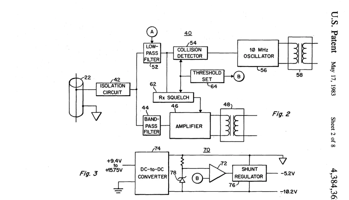
FIG. 1 is a block diagram of the transmitter portion of The rules of such a network (Le., ~ts communic~ti~ns the transceiver of the present invention; 20 protocol) normally defin~ a maxImum transm~sslon FIG. 2 is a block diagram of the receiver portion of packet length, at least partIally for th~ purpose ofmsur-the transceiver of ofmsur-the present invention; mg that one. user does n?t monop?hze .the chan~el. If
FIG. 3 is a block diagram of the power supply for the the host deVIce at a partIcular ~tatlon. vIolates thIS rule . transceiver of the present invention; fo~ som
7
reason, or the cable dnver stIcks on andtrans-FIG. 4 is a schematic circuit diagram of the signal- 25 mlts n?lse or a d.c. level aft~r th~ host has stopped t· t' f th t 'tt f FIG 1 supplymg a message, guard sWItch tImers 28 and guard genera mg por Ion 0 e ransml er 0 . ; , h 26 'd ~ d' ' h .
FIG. 5 is a schematic circuit diagram of the guard SWltC es pr?vI e a means or Isconnectmg t e m-•. 't 25 f FIG 1 ' volved transceIver from the network so that other users
ClrcUl ry, 0 ' , ; " . , a r e not unduly inconvenienced. This isolates the prob-FIG, 61s a schematIC CIrcUIt dIagram of the transmlt- 30 I t the st t' h'ch h d 't To thl' d I h d f " d d 11" em 0 a IOn.w I as cause I. S en , ter sque. c , en -0 -transmISSIOn etector an co ISlon- guard driver 32 uses the transmitter squelch signal as an detect slII~ulator bloc~s o~ FI~. ~; . . indicator of transmitter activity and starts the guard FIG. 7 Is.a schematic CIrCUIt dIagram ~f the c~lhslOn switch timers running at the start of each transmission. detect, r~celve squelch and threshold settmg portIOns of After the time defined by the guard switch timers 28, the recel,,:er of FIG.~;, , , 35 the guard switches 26 are turned on, shorting the output FIG. 81s a s~hematlc ~trCUlt dIagram ~fthe band-pass current of cable driver 20 to ground and thus effectively filter and ~mphfier po~tto~s o~ th~ receIver of FIG. 2; removing the transmitter from the network.
, FIG, 9 IS a schematic CIrCUIt dIagram of the d.c.-to- The transceiver is further provided with circuitry for d.c. conver~er of FIG. ~; a~d. , testing its collision detection circuitry. This is done by a FIG. 10 IS a schematIC cIrcuIt dIagram of the power 40 collision detector test mechanism 34. The collision de-supply regulator of FIG. 3. tector test mechanism functionally comprises an
end-of-DETAILED DESCRIPTION OF AN ILLUSTRATED EMBODIMENT
Referring now to FIG, 1, there is shown a block 45'
diagram of the transmitter portion of the transceiver of the present invention. The computer or other host de-vice (not shown) which communicates via the trans-ceiver supplies information to be transmitted over lines 12A and 12B to the primary winding of an input trans- 50 former 14. The secondary winding of transformer 14 -,feeds a buffer amplifier 16 and a transmitter squelch circuit 18. Buffer 16, in tum, feeds a cable driver circuit 20.
. The cable driver 20 is a current source which gener- 55 . ates the transmit signal applied to the coaxial cable 22
through an isolation circuit 24,
The transmitter squelch circuit 18 monitors the sec-.ondary winding of transformer 14 to determine whether
the host is sending any signal for transmission. When no 60 signal is being supplied, transmitter squelch 18 disables cable driver 20 so that no spurious information will be transmitted.
Isolation circuit 24 prevents a short circuit in the transmitter from shorting out the cable. As will be ap- 65 parent from the discussion below, other circuitry in the transceiver intentionally may short out the transmitter or a component failure may do so.
transmission detector 36 and a collision simulator 38. The end-of-transmission detector 36 monitors the trans-mitter squelch signal for a change of state indicating the termination of a transmission, at which time it actuates the collision simulator 38. The collision simulator feeds
a:
signal into the receiver section of the transceiver (at point A, as indicated in FIG. 2). If the collision detec-tion circuitry in the receiver is operating properly, it will signal a collision to the host device. Due to the timing of the collision signal relative to the end of the transmission, the host computer knows to recognize it as a validation of the test. Conversely, it knows that if the collision signal does not appear, the test was failed and the transceiver should not be used for transmision until it is repaired.5
4,384,363
6
rather than an abrupt leading and falling edge transition. Thus, from a square wave input, the cable driver 20 generates a well-controlled symmetric trapezoid wave-form, through a two-pole RC network which gives a 25 signals to or from the host must be transformer-coupled
due to the need for electrical isolation among hosts.) A receiver squelch circuit 62 interconnects the two paths, and gates on the receiver only in the presence of a valid
signal. 5 ns rise-time. This gets rid of much of the high frequency energy in the binary waveform without phase-distorting the zero crossings. If a square wave had been used, rather than a staircase, larger filter capacitors would Low-pass filter (LPF) 52 time-averages the received
signal, to provide a d.c. signal indicative of whether information is being transmitted on the cable 22. The output of the collision simulator 38, since it mimics the presence of more than one transmitter signal on the line, 10 is supplied as a second input to LPF 52. Collision detec-tor 54 is a threshold detecdetec-tor which monidetec-tors the output of low pass filter 52. If the LPF output exceeds a prede-termined threshold, corresponding to the presence of more than one active transmitter, a collision is indicated 15
and the 10 MHz oscillator 56 is then turned on to signal collision detection.
Receiver squelch circuit 62 also responds to the out-put of LPF 52 by providing a squelch signal to amplifier 46. The squelch signal turns off amplifier 46 when the 20 output of the LPF 52 is so low as to indicate that no signal is being received.
It will be appreciated that the proper operation of collision detector 54 and receiver squelch circuit 62 require the use of stable, accurate thresholds. They are 25
provided by a threshold setting network 64. In addition to the threshold voltages supplied to the collision detec-tor and receiver squelch, the threshold setting network 64 also provides a feedback signal (at point B) whose value is proportional to the threshold signal. This feed- 30
back signal is sensed by a comparison amplifier 72 in the power supply 70 (shown in FIG. 3), to control one of the two power supply output voltages.
Power supply 70, in FIG. 3, employs a d.c.-to-d.c. converter 74 to generate a -10.2 volt d.c. supply from 35
a host power supply of +9.4 to + 15.75 volts. In addi-tion, a shunt regulator 76 provides a -5.2 volt supply derived from the -10.2 volt source. The shunt regula-tor 76 is controlled by a comparison amplifier 72 which compares a voltage established by zener diode 78 with 40 the feedback voltage generated at point B in the thresh-old setting network 64 of FIG. 2. Thus, the actual out-put level of the nominally - 5.2 volt supply is adjusted and regulated so as to maintain the feedback voltage at point B equal to the voltage established by zener diode 45 78. Consequently, the output of regulator 76 may be greater or less than -5.2 volts, as required to provide precision setting of the threshold by the threshold set-ting network 64.
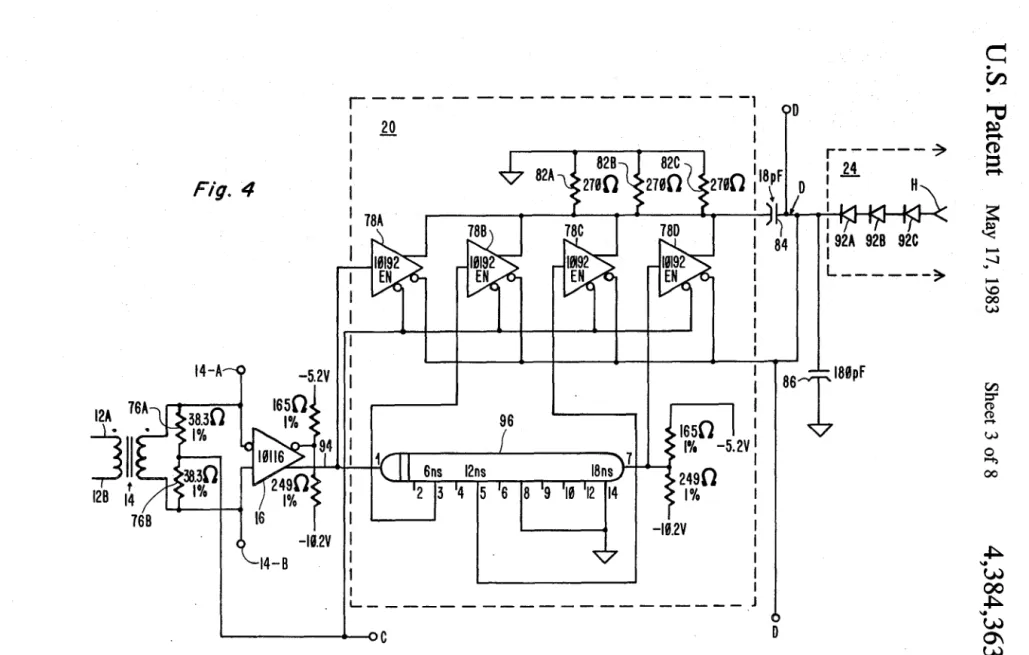
FIG. 4 shows the basic circuitry for the transmitter of 50 the transceiver. The signal to be transmitted is applied to the primary winding (i.e., leads 12A and 12B) of a transformer 14. The secondary winding of transformer 14 provides the input of a buffer amplifier, or line re-ceiver 16. A pair of matched resistors 76A and 76B are 55 also connected in series across the secondary winding of transformer 14, for impedance matching. A center tap is . provided at the junction of the two resistors 76A and 76B, and is labelled point C. Point C is connected to a similarly labelled point on FIG. 6, at the output of the 60
squelch circuit. The non-inverting output of buffer am-plifier 16, on line 94, provides the signal input to the cable driver 20.
Cable driver 20 is a current source which may be turned on and off to drive the coax cable channel with 65 a binary waveform. The output from cable driver 20, however, is not simply a square wave type of output. It has been found desirable to provide a staircase ramp
have been needed, thus causing unacceptable phase distortion.
In the exemplary embodiment in FIG. 4, cable driver 20 is implemented with four stages, 78A-78D, provid-ing four steps to the risprovid-ing and fallprovid-ing staircase. Of course, a different number of steps also can be em-ployed; the number of stages to be used is at the design-er's discretion, and four has simply been found conve-nient. Each of the stages is a differential current switch having a signal input, non-inverted and inverted out-puts, and a control (i.e., enable/disable) input. Except for the signal inputs, the current switches 78A-78D are connected in parallel, with like terminals connected to each other. Their non-inverted outputs are all con-nected to a resistors 82A-82C, which connect to ground, and to one lead of a first filter capacitor 84. The inverted outputs of current switches 78A-78D are con-nected to the other lead of capadtor 84, which connec-tion also provides the cable driver output, at point (or node) D. There are four other connections to node D, as well: (1) a second filter capacitor 86, connected be-tween node D and the transceiver ground; (2) a series string of three diodes 92A-92C connected between node D and the coaxial cable, comprising isolation cir-cuit 24; (3) guard switches 26, connected from node D to ground; and (4) a transmit bias current switch, shown in FIG. 6.
The enable/disable terminals of the current switches 78A-78D receive an enable/disable signal at point C, from the transmitter squelch circuit of FIG. 6.
In isolation circuit 24, three diodes are connected in series to protect against the possibility of one, or even two diodes short circuiting. Should point D be grounded, diodes 92A-92C become back-biased (open circuits) during other hosts' transmissions, thereby iso-lating the transmitter from the network. Conversely, the sole result of an open diode is to cause single station failure, while leaving the network intact. The isolation network provides important protection, because the transceiver is direct coupled to the network cable.
7
4,384,363
8
82A-82C and capacitors 84 and 86 provide a two-pole essary to the understanding of this invention. The RC filter for smoothing the output signal. squelch circuit monitors the transmit signal from the Referring now to FIG. 5, guard circuits 25A-25C for host (which appears across points 14-A and 14-B, the shorting the output of the cable driver 20 are shown. secondary leads of transformer 14) and provides two The guard circuits comprise a plurality of switches 5 outputs, the cable driver enable/disable signal which is 26A-26C connected in parallel, each having one termi- provided on line 156 (point C) and the complement to nal connecting to the transceiver ground and the other that signal which is provided on line 158.
terminal connected to node D. The switches are all Transistors 162 and 164 comprise an emitter-coupled controlled by a common driver 32 (gate 108 and transis- pair. The base of transistor 162 is driven by the non-tor 112); and the driver is operated by a signal supplied 10 asserted output of amplifier 154, on line 156. The collec-at point E, which indiccollec-ates the start of each transmis- tor of transistor 162 supplies an output signal at connec-sion. tion point E, which connects to a similarly labelled
In the exemplary embodiment, the transceiver uses point on FIG. 4 to drive the guard circuit driver. The three guard circuits 25A, 25B and 25C, connected in signal at point E is essentially an inverted and level-parallel. The guard circuits are identical to one another. 15 shifted representation of the signal on line 156. The number of guard circuits employed is at the design- Transistor 164 is driven at its base by the asserted er's discretion, since multiple guard circuits merely output of amplifier 154, on line 158. The collector of provide redundant protection and reduce the statistical transistor 164 provides a transmit bias which is con-probabilty offunctional failure in the transceiver which nected to point D on FIG. 4. During transmission, tran-"brings the network down." When three guard circuits 20 sistor 162 is turned off and transistor 164 is turned on. are employed, of course, the chances of them ail being The signal on line 158 from amplifier 154 also feeds out of commission is much lower than the chance for transistor 172 through capacitor 174 and resistors 176 one guard circuit alone being out of commission. and 178. At the end of a transmission, when the squelch Since all of the guard circuits are identical, only changes state, a spike or pulse approximately one micro-guard circuit 25A will be explained in detail, it being 25 second wide is produced at the emitter of transistor 172 understood that the same explanation applies with re- due to the effect of differentiation produced by capaci-spect to the other guard circuits. tor 174. This turns on transistor 182 for a like duration
Guard circuit 25A comprises a guard switch 26A and and produces a collision test signal at the collector of a guard switch timer 28A, which includes transistors transistor 182, which is shown as a point F to be con-102A, 104A and 106A, plus their associated compo- 30 nected to a similarly marked point on FIG. 7, in the nents. Guard switch transistor 26A is connected as a low-pass filter of the receiver.
simple common emitter switch with its emitter attached The collision test signal simulates the effect of a colli-to the transceiver ground and its colleccolli-tor attached colli-to sion by drawing excess current through the receiver the node D of FIG. 4. When actuated, the switch tran- input at the end of every packet transmitted. Transistor sistor 26A shorts out node D to ground. It is open only 35 204 isolates the collision test signal from the network, so when there is a valid signal to transmit. A guard circuit it is not seen by other stations; only the transmitting driver comprising OR/NOR gate 108 and transistor 112 station responds to it. Further, this collision test does controls the operation of guard switch timer 28A. not suffer from "single point of failure" problem. The A "stuck on" current switch 78A-78D will draw host, of course, must check at the end of each transmis-current from the guard switch(es) rather than the net- 40 sion for the presence of the "collision signal" generated
work. by the collision test signal.
When the signal at connection point E from the trans- Attention is now directed to the aforesaid FIG. 7, mitter squelch circuit of FIG. 6 changes state to indicate which illustrates the low-pass filter, receiver squelch, the beginning of a transmission (i.e., it goes high), tran- . collision detector, collision oscillator and threshold sistor 112 emitter goes low and diode 116 becomes back 45 setting circuits. Connection point H is the receiver input biased, allowing resistor 122 to discharge capacitor 118. from the coaxial cable (and, of course, the transmitter Resistor 122 controls the rate at which capacitor 118 output, as well). It is attached to a fusible resistor 202 discharges. When capacitor 118 is discharged suffi- which provides protection against a short circuit in ciently, the voltage across it turns off transistor 104A. transistor 204 having any adverse impact on the net-Transistors 104A and 106A are an emitter-coupled pair, 50 work. Transistor 204 is connected as a unity gain emit-so when transistor 104A turns off, transistor 106A turns ter-follower. A current source comprised of transistor on, activating switch 26A and driving transistor 26A 206 and resistor 208 biases transistor 204 so that it is into saturation. Thus, a predetermined time after the always conducting.
4,384,363
10
236 and to the inverting input .~8 of !lsimilar compara- capacitor 308 and resistor 312, on the non-inverting input of a differential line receiver amplifier 314.
The output of amplifier 314 feeds another buffer plifier stage 316. The receiver squelch signal from am-tor 242. The signal on,line 232 }ssupplied to the
non-inverting input 244 of comparator 236 and, through a resistor 246 to the,non-inverting input 248 of compara-tor 242.
The two thresholds are set by a precision current source comprising transistor 252 plus a compensation circuit comprising transistors 258 and 262. The base of transistor 252 is connected to the - 5.2 volt supply and
5 plifier 274 (connection point K) is also connected to the output of buffer amplifier 316. Since this is emitter-cou-pled logic, if the output of either amplifier 274 or ampli-fier 316 is high, then their common connection (point its emitter is connected. to the -10.2 volt supply 10
through a resistor 264. Resistor 264 is a high precision resistor; the voltage across it sets the emitter current of transistor. 252. The power supply adjusts the precise value of the regulted output (which is nominally -5.2 volts) to achieve the desired current through resistor 15
264. To this end, the voltage at the emitter of transistor 252 is sensed by the power supply and a connection to the power supply is shown at a point labelled B. Tran-sistor 258 is connected as a similar current source with an emitter resistor 266 having the same value as resistor 20 264, to produce the same emitter current.
Transistor 262 is the. load for current so.urce 258 and its sole purpose is to draw a base current into transistor 262 which, will raise the current drawn through resis-tors 268 and 272 by an amount which very nearly equals 25 the difference between the collector current and emitter current of transistor 252. Thus, transistor 262 is in-tended to compensate for the fact that transistor 252 has a finite current gain as a result of which its collector current does not exactly equal its emitter current, by 30 pulling a current through resistors 268 and 272 which is very close to the emitter current through resistor 264.
Preferably, transistor 252 and 262 will be provided on the same substrate so as to provide matching current gain, and thereby.set the current in resistors 268 and 272 35 exactly equal to the emitter current of transistor 252. The actual threshold voltages are developed across resistors 268 and 272 plus the sum of the base-emitter drops across transistors 254 and 156. Transistors 254 and 256 are used to match the corresponding base-emit- 40 ter drops of transistors 214 and 204.
Preferably, transistors 256 and 204 will be provided on the same substrate so that their base-emitter voltage drops will match and transistors 254 and 214 will also be provided on the same substrate, for the same reason. 45
The signal provided on line 232, to be compared with the reference thresholds, is produced by filtering the sum of the signal received over the coaxial cable and the collision simulation test signal supplied at point F.
The comparator 236 drives a buffer amplifier 274, the 50 output of which provides the receiver squelch signal at point K, which is connected to the similarly labelled point in FIG. 8.
The comparator 242 detects whether the collision threshold has been exceeded. In tum, it drives a buffer 55
amplifier 276 which turns on and off a 10 MHz oscilla-tor formed by ORINOR gate 278, capacioscilla-tors 282 and . 284, inductor 286 and resistor 288. The ORINOR gate 278 provides a balanced output for driving a trans-former 292 through which a collision presence signal is 60 supplied to the host device.
Turning now to FIG. 8, the receiver circuitry will be explained in detail. The receiver gets its input at point L, the emitter of transistor 204 in FIG. 7. Resistor 302 and capacitor 304 filter out the high frequency compo- 65
nents in the received signal. Transistor 306 is an emitter follower which acts as a buffer and provides a low impedance output to drive a high pass filter comprising
K) is high. Thus, the output of amplifier 316 is squelched, or turned off, by maintaining the output of amplifier 274 high.
The o:utput of amplifier 316 also feeds the non-invert-ing input of another amplifier stage 318, which then feeds an ORINOR gate 320. Gate 320 provides gain and also presents a balanced differential output signal to drive a transformer 322 through which the receive signal is communicated to the host device.
In FIG. 9, circuitry is provided for a d.c.-to-d.c. con-verter useful in the power supply of the present inven-tion for converting +9.4 to + 15.75 volt power from the host or other source to - 10.2 volts. The details of the d.c.-to-d.c. converter are unimportant in terms of understanding the present invention; other converter circuits could be employed just as well and the design of power supplies, including the design of such converters, is well-developed in the electrical arts. Thus, for pur-poses of this explanation, it is sufficient to note that the d.c.-to-d.c. converter 74 receives a positive voltage at terminal M relative to an input power return, or ground, at terminal N and that it supplies an unregulated output voltage at a terminal· P relative to an isolated transceiver ground at terminal R. A co-operating voltage regulator shown in FIG. 10, is connected to terminals P and R. This voltage regulator also supplies a feedback signal to a point S in .the converter, responsive to which the d.c.-to-d.c. converter adjusts its output voltage.
Turning now to FIG. 10, the regulator circuitry is shown for taking the unregulated voltage supplied at terminal P and providing regulated outputs of -10.2 and - 5.2 volts.
A 4.3 volt zener diode 78 is connected across the 10.2 volt supply through a series 590 ohm resistor 358, to provide a precise reference point 4.3 volts above (i.e., more positive than) the nominally -10.2 volt supply, at the non-inverting input 359 of operational amplifier 360. A precision resistive divider network 362 and 364 is designed to provide 4.3 volts at the inverting input 366 of amplifier 360 when the voltage across terminals point R is precisely 10.2 volts. The output of amplifier 360 provides a feedback signal to the d.c.-to-d.c. converter 74, at point S. The feedback signal supplied to point S represents the error between the 4.3 volt reference pro-vided by zener diode 78 and the voltage measured at the inverting input of amplifier 360, and, thus, the amount by which the voltage at terminals P, R differs from 10.2 volts. The d.c.-to-d.c. converter 74 responds to the feedback signal at point S by adjusting its output so as to eliminate any error signal.
11
4,384,363
for the threshold-setting network. The output of ampli-fier 72 controls a shunt regulator comprised of transis-tors 372 and 374, as well as capacitransis-tors 376, 378, 382 and 384, to provide a regulated -5.2 volt output at point T. The resulting precise regulation is at point B, where it 5 has direct effect on the precision of threshold-setting.
Amplifier 72 senses a point remote to the power sup-ply itself, where a specific voltage (equal to the zener diode voltage) should appear; it compares the sensed voltage with the reference voltage established by the 10 zener diode and drives the shunt regulator output to force the remote, monitored voltage to equal the refer-ence voltage. Any deviation between the two produces an error signal which causes either transistor 372 or 374 to be driven harder, thus shifting the electrical position 15
of their emitter connections relative to the 10.2 volt supply.
This circuit thus permits a single zener diode refer-ence to be used to regulate two different supply volt-ages, one in the power supply and the other in one of 20
the circuits powered by the supply.
Having thus described the invention, it will be appar-ent that various modifications, alterations, and improve-ments will readily occur to those skilled in the art. Ac-cordingly, it is intended that such alterations, modifica- 25
tions and improvements as are obvious herefrom be included within the scope of this invention. The inven-tion is intended to be limited only as defined in the appended claims, the foregoing description being illus-·trative only, and not limiting. 30
Having illustrated and described my invention, I claim:
1. In a transceiver for a station of a carrier-sense multiple access network with network access con-trolled by collision detection, wherein the transceiver 35 includes a transmitter and a receiver, the transmitter
40
45
50
55
60
65
12
iricludes a current source output stage, the receiver includes collision detection means for detecting the presence of two or more stations in the network trans-mitting simultaneously, and the transmitter current source and receiver collision detection means are cou-pied via a coaxial cable which provides a communica-tions channel for the network, the improvement com-prising:
the transmitter current source being constructed of emitter-coupled logic which requires d.c. power within a first, specified voltage range and an output voltage not exceeding a level at which the current source circuitry becomes a Voltage source, such level being termed the compliance limit of the current source;
the receiver's collision detection means requiring d.c. power within a second voltage range;
first power supply means for supplying voltage within the first range;
second power supply means for supplying voltage within the second range; .
the first range extending between a first voltage and a second voltage;
the second range extending between said second volt-age and a third voltvolt-age; and
the third voltage also being the voltage on the coaxial cable with no signal imposed thereon;
whereby the voltage swing at the output of the trans.. mitter current source can extend from the third voltage to the compliance limit of the transmitter current source, which is in the first range, in the event of a collision between two or more transmit-ters, thereby preventing saturation of the current source and making the collision condition detect-able by the collision detection means.