http://wrap.warwick.ac.uk/
Original citation:Chown, P. (1990) Notes on the design of a barrel shifter for the Warwick pipelined CORDIC processor. University of Warwick. Department of Computer Science. (Department of Computer Science Research Report). (Unpublished) CS-RR-161
Permanent WRAP url:
http://wrap.warwick.ac.uk/60856
Copyright and reuse:
The Warwick Research Archive Portal (WRAP) makes this work by researchers of the University of Warwick available open access under the following conditions. Copyright © and all moral rights to the version of the paper presented here belong to the individual author(s) and/or other copyright owners. To the extent reasonable and practicable the material made available in WRAP has been checked for eligibility before being made available.
Copies of full items can be used for personal research or study, educational, or not-for-profit purposes without prior permission or charge. Provided that the authors, title and full bibliographic details are credited, a hyperlink and/or URL is given for the original metadata page and the content is not changed in any way.
A note on versions:
The version presented in WRAP is the published version or, version of record, and may be cited as it appears here.For more information, please contact the WRAP Team at:
Research report 161
NOTES ON THE DESIGN OF A BARREL SHIFTER FOR THE WARWICK PIPELINED
CORDIC PROCESSOR.
PAUL CHOWN
(RR161)
Notes on the design of a Barrel Shifter
for the Warwick Pipelined CORDIC processor
Paul Chown
VLSI Architectures Group February 1989
Abstract
This document discusses the design decisions made during the design of the barrel shifters used in the floating point adjustment circuitry of the Warwick pipelined CORDIC processor. The barrel shifter is required for both the input (mantissa alignment) and output (post normalisation) parts of the floating point data path, although it also has applications in other areas such as bit field extraction and multiplication / division. A brief survey of the available techniques will be given, followed by a discussion of the design process for the Barrel Shifters in our implementation of the CORDIC algorithm.
LI
Project Background
The design of the Warwick Pipelined CORDIC processor took a period of approximately six months, largely due to the regularity of the design. The algorithmic work on which the processor was based had already been carried out by Kieran Lismore and John Vaudin and a sequential integer version of the CORDIC algorithm implemented in silicon [Vaud86]. This work has been continued to produce a pipelined implementation of the algorithm supporting 32 bit floating point arithmetic. The result of the design effort to date has been a layout for a 1cm by 1cm integrated circuit produced using the MAGIC layout system from Berkeley with the design rules for the ES2 21.tm e-beam process. The individual cells and some larger sections of circuitry have been simulated using SPICE, and logic level simulations carried out to verify larger scale behaviour. We now intend to produce a small test IC which will be used to study the exact operation of the circuit elements and to test some novel circuit techniques that may be used in a later version. The complete design of the CORDIC processor will be described elsewhere [Chown90]. This paper will focus on the techniques used to design the shift units required on the processor.
Barrel Shifter Functionality
There are two forms for the Barrel Shifter circuit. The first is a full Barrel Shifter or rotator in which bits shifted out of one end of the input word re-enter the word 'at the opposite end. The second is a simple shifter in which the bit positions vacated by the shift are filled with predetermined values, unaffected by the bits lost at the other end. These values may be data dependant, however, such as in the design of a two's complement shifter which must be capable of performing sign extension.
In the remainder of this document, the term Barrel Shifter will be used when referring to a network that implements a rotation, and Simple Shifter or
Shifter by itself will refer to a network that implements a shift where bits are lost
from the ends of the input. Where no distinction is drawn between the two types of shifter it should be assumed that the comments made can be applied to both.
Barrel Shifter Design
Topological Considerations
A major factor to be considered before embarking on the design of a shift unit is the relationship of the shifter to the other circuitry of the processor on which it is to be placed. This may be understood by roughing out a floorplan for the processor with estimated sizes for the functional units and routes for the main data paths. By determining in this way the desired shape of the shifter and the direction in which the data is to flow through it, the design may be made more area (and time) efficient. The pitch of the input and output signals of the shifter may also be estimated at this stage. For a large number of data lines, a change in direction or line pitch brought about by insufficient planning at an early stage may lead either to an almost equal area being required to correct the mistake, or a large redesign period, both for the shifter and possibly the surrounding circuits. There are three possible options for the relationship between the inputs and outputs given the Manhatten layout scheme used in many MOS designs :
• Right-angle turn • Straight through
• Loop back (in & out on same side)
Each of these topologies and those available under more flexible layout schemes have various advantages and disadvantages, but the essential point in them all is that wherever possible the topology should match the direction in which the data lines would go were the barrel shifter not there. If this is not the case then it will be found necessary to use additional chip area to correct the deviation.
Design Requirements
Several different schemes have been proposed for the implementation of barrel shifters, each attempting to produce a balanced, efficient design technique. In order to produce a complete design, the bounding limits on power, speed and area will need to be defined before the choice of a particular implementation can be made.
Design Choices
Choice of Size
The choice of the size of shifter to implement (i.e. the number of different shifts allowed) will be largely dictated by the utilisation of the shifter in the final application and the area of silicon that is therefore available for the implementation of the shift operation. The justification for putting a full shifter onto a chip must be made in relation to the cost of that implementation in terms of overall processing speed, according to the reasoning of Hennessy and Patterson in their quantitative work on the design of processors [Henn90]. In some cases it may be more suitable to implement a circuit to perform a partial shift of a few bits (e.g. 0..8) and repeat this operation several times in order to perform the full shift, rather than putting a full shifter onto silicon. An example of this approach can be found in the design of the shifter for the MicroVAX floating point unit [Simc86].
By making proper selection of computational algorithms and concurrent operations within a processor, it may be possible to either restrict the number of different shifts required, or to use a single shifter in more than one type of operation, allowing greater usage and consequently greater area available for the implementation. These decisions are obviously different for every implementation and need to be considered carefully before design work is started.
The area taken by a barrel shifter increases linearly according to both the number of bits of the input number and the number of shifts that are available from the shifter. This means that a shifter providing all of the n shifts of an n bit word in a single direction will increase in area according to an 0(n2) law.
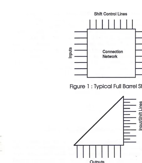
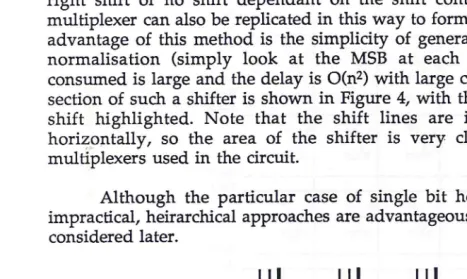
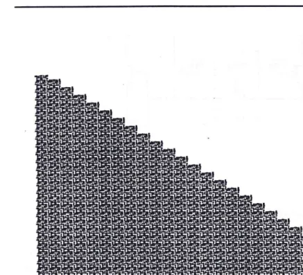
Full Barrel or Shifter ?
In the case of a Barrel Shifter each input can be switched to each of the outputs, leading in the naive case to n2 switches. In the case of a simple shifter each input is connected to on average n/2 of the outputs, leading to n2 / 2 switches. Intuitively therefore, a simple shifter should occupy half of the area of a barrel shifter, although the shape of a simple shifter may mean that this area saving cannot be effectively utilised by other circuits on the chip. This is demonstrated by figures 1 and 2 which show the areas required by two different types of shifter. It can be seen that if two shifters of the triangular form are required then it may be possible to place them back to back, obtaining maximum usage of the triangular area that may otherwise remain unused.
Barrel Shifter Design
Shift Control L nes
I I I 1 1 1 1 1
[image:8.842.82.536.100.621.2]Connection Network
Figure 1 : Typical Full Barrel Shifter
0) 7 1:1_ C
np
u
t/Shift
Lines
I I 1 I I I I I
Ou pu s
Figure 2 : Simple Shifter with Right Angle Turn
Static or Dynamic ?
The choice of a static design implies that both high and low signals will need to pass through the switches forming the shift network and for a CMOS technology this will be best carried out using transmission gates as the switching nodes. Unfortunately these will require both true and inverted shift control signals to be supplied to each switch, and both n- and p- type subtrates to be present within the array. This will lead to large area requirements for the switching array. The large capacitive loads placed on the data lines in this case are also a problem. Single transistor switches can be used (for example in nMOS) but the speed of the circuit will be hampered by the voltage drop across the single transistor and its higher resistance. Figure 3 shows typical figures for the resistances of various switching methods, taken from the 2gm ES2 CMOS design rules using transistors of 4p.m channel width in all cases.
Switch Resistance
Tx Gate 6.9k0 nMOS 9.9k0 pMOS 23.3kS2
Figure 3 - Typical Switch Resistances (ES2 2p.m CMOS)
A dynamic design requires a Precharge period in which the entire shift array can be charged to a given logic level. This may be overlapped with the generation of shift control signals and charging of the shift lines, and with operations being performed elsewhere in the chip. When the Precharge period has ended then the outputs are selectively discharged by the input drivers under the control of the shift signals. The fact that only one logic level is being driven through the switches means that a single transistor (and consequently one shift line) may be used to form each switch, leading to large area savings. This is partly offset by the more complicated drivers necessary for precharged operation. The speed up of the shift operation due to reduced capacitances and shorter data lines may be lost if the precharge period cannot be offset against another operation within the processor.
Barrel Shifter Design
Another problem with the design of dynamic shifters is the possibility of crosstalk between the lines of the shift network. Since the lines within a shift network are long, often running in parallel, and not connected to a voltage source other than in the precharge phase, they are prone to crosstalk when the selective discharge is taking place. The possibility of this should be borne in mind when laying out the cells for the network, to reduce the capacitive coupling between input and output lines.
Design of Switching Networks
Heirarchy of single-bit up/down shifters
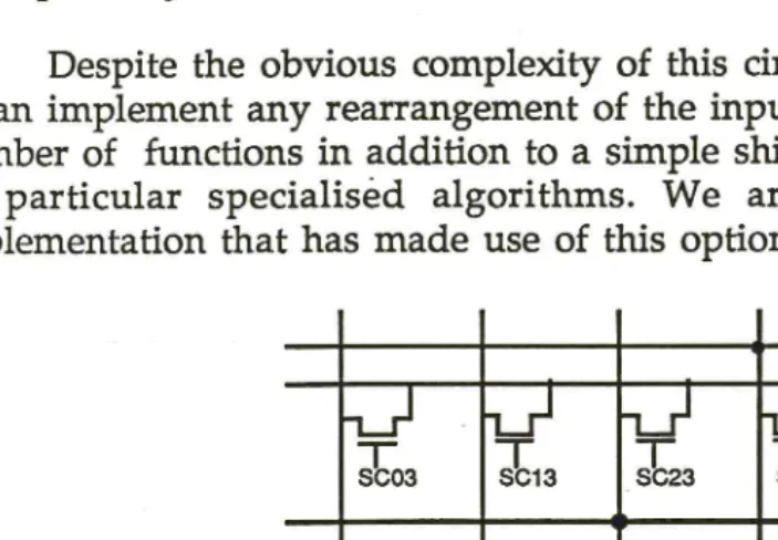
Single bit multiplexers can be used to shift a data word by using n layers of n single bit 3-1 multiplexers each layer of which implements a single bit left shift, right shift or no shift dependant on the shift control input [Mead80]. A 2-1 multiplexer can also be replicated in this way to form a unidirectional shifter. An advantage of this method is the simplicity of generating shift signals for post-normalisation (simply look at the MSB at each level). However the area consumed is large and the delay is 0(n2) with large capacitances at each stage. A section of such a shifter is shown in Figure 4, with the data path taken for a left shift highlighted. Note that the shift lines are interleaved as they travel horizontally, so the area of the shifter is very close to the area of the n2 multiplexers used in the circuit.
[image:10.842.73.541.462.741.2]Although the particular case of single bit heirarchical shifters appears impractical, heirarchical approaches are advantageous in other forms that will be considered later.
Simple Crossbar Switch
Since every input bit must be able to appear at every possible output position, the full Barrel Shifter can be considered as a crossbar switch as shown in Figure 4 [Mead80]. This circuit implements a barrel shift in nMOS technology and can be modified to perform a simple shift by removing transistors either above or below the diagonal running from bottom left to top right. Each shift control line SCxy indicates that input Bus X is to be connected to output Out Y. The disadvantage is that n2 shift control lines must be generated and distributed, corresponding to the n2 switches that are required.
Despite the obvious complexity of this circuit and its control mechanism, it can implement any rearrangement of the input signals and so may provide a number of functions in addition to a simple shift. These functions may be used by particular specialised algorithms. We are not currently aware of an implementation that has made use of this option, however.
•
1—ii
-1-
SC33
1—1
1- scoo I— T
SC13 i—r 7 SC23 • -LSI T SC22 -L2-1 -1- SC32 7
SCO2 T SC12 •
•
7 sc oi T sc,
1 7 SC21 -SC31 I-
]
T T T
[image:11.842.107.459.319.563.2]SCOO SC10 SC20 SC30
Figure 5 - Crossbar Switch for Shifting
Modified Crossbar Switch
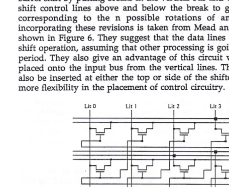
When performing simple shifts on data values as opposed to general rearrangement of inputs, only a subset of the possible connections provided by a Crossbar Switch are utilised and so rather than generating the n2 shift control lines required by Figure 5, 2n-1 shift signals are generated (corresponding to the 2n-1 possible shifts of an n-bit word). These shift signals are routed to a number of gates to activate a given shift, in the case of Figure 5 these are the diagonals running from top right to bottom left.
Barrel Shifter Design
This simplified form of control can also be used to carry out a rotation or barrel shift by putting breaks in the vertical bus and wiring together the diagonal shift control lines above and below the break to give a total of n shift lines corresponding to the n possible rotations of an n-bit input. The circuit incorporating these revisions is taken from Mead and Conway [Mead80] and is shown in Figure 6. They suggest that the data lines be precharged to speed the shift operation, assuming that other processing is going on during the precharge period. They also give an advantage of this circuit which is that literals can be placed onto the input bus from the vertical lines. The shift control signals may also be inserted at either the top or side of the shifter which allows for slightly more flexibility in the placement of control circuitry.
Lit 0 Lit 1 Lit 2 Lit 3
Bus A 3 Out 3
Shift 3 Bus B 3 Bus A 2 Out 2
Shift 2 Bus B 2 Bus A I Out 1
Shift I Bus B 1 Bus A0 Out 0
Shift 0 Bus B 0 ■
-L_F -7_1 L_FT __T
TFT T T •
■
T TT TT F -r T •
TFTFT T r-
I
Shift 3 Shift 2 Shift 1 Shift 0
[image:12.842.78.535.172.546.2]•
Figure 6 - Modified Crossbar Switch
Weste and Eshraghian. [West88] give a similar circuit to that of Mead and Conway, although the inputs in this case arrive at two edges. They also extend the nMOS shifter to CMOS using transmission gates as network switches and demonstrate a possible layout. Functionally the circuit is the same as that already described. Once again a precharged version is suggested which allows us to dispense with the p-transistors from the CMOS version of the shifter.
Heirarchical Shifters
Peng, Samudrala and Gavrielov [Peng871 describe a simple triangular shift circuit with a right-angled turn of the data lines which avoids the additional turn implemented by the circuit of Figure 4, giving its straight-through topology. They also suggest a precharging scheme to speed the operation of the circuit, given certain timing conditions for the data and shift lines.
This triangular shifter is then combined with the idea of a heirarchical approach using two levels of shift to obtain all of the possible shift combinations. The example they use is an 8 bit data word which is first shifted through either 0 or 4 bit positions and then in a second stage through 0,1,2 or 3 bit positions. In this way, any shift in the range 0..7 may be realised by an appropriate combination of the two shifts. The method does not require full decoding for the shift control signals and reduces the capacitive loading on the data lines of the network. This is accomplished at the expense of increasing the number of transistors through which the signals must pass (previously 1), complicating the precharging and counteracting some of the capacitive savings.
Anderson, Earle et. al. [And671 use the same approach in the IBM System/360 Model 91 shifter, using two level shifts of (0,1,2,3) and (0,4,8,12) bits respectively to shift a 14 bit data word. No discussion of the design tradeoffs involved is made here, however.
Barrel Shiffer Design
Feedback techniques
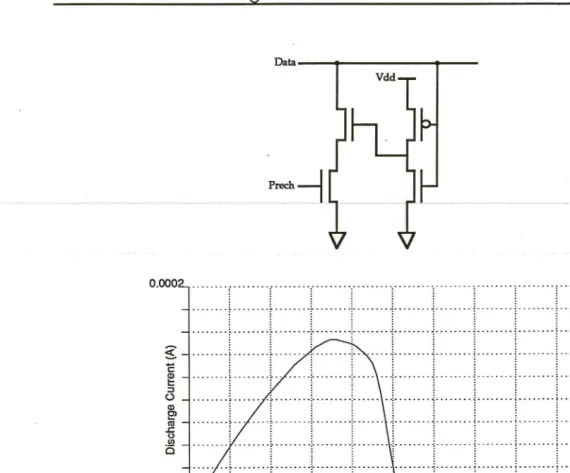
One of the problems facing the designer of a shift circuit is the noise susceptibility and capacitive delay that arise from driving long data lines through pass transistors. Some output data lines may well be disconnected from any current source or sink, causing additional sensitivity to capacitive coupling. A number of sources demonstrate methods to aid the designer in this situation, by adding circuitry to the data line itself to make it an active responder to the driving signal. An example of such a circuit is given in Figure 7, taken from Heron and Kruckenberg [Her90]. The circuit reacts to a voltage change on the Data line by sinking current to ground, hopefully speeding up the discharge. The circuit operates under a precharged circuit scheme and the 'Prech' line in the circuit is used to disable the feedback circuit while the Data line is being precharged.
Data
Vdd
Prech
0.000
arg
e
Curren
U N
[image:15.842.25.596.72.545.2]Data Line Voltage (V)
Figure 7 - Feedback Circuit for Data Lines
Arrangement of a Heirarchical Shifter
There are two factors that affect the operation speed of a barrel shifter circuit, each modifying the behaviour of a typical shift path through the switching network. These factors are :
• The resistance arising from both the data lines themselves and the switches through which they pass
• The capacitance arising from both the data lines themselves and the source/drains of any FET's to which they connect.
The distribution of these resistances and capacitances will play a great part in determining the performance of the circuit. Obviously the design of the drive and sense circuitry will also be an important factor, but it will be assumed here that any changes made to these will still be reliant on the performance of the shift network itself.
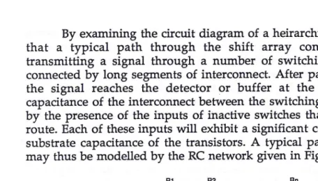
Barrel Shifter Design
By examining the circuit diagram of a heirarchical shift unit, it can be seen that a typical path through the shift array consists of a voltage source transmitting a signal through a number of switching nodes, the nodes being connected by long segments of interconnect. After passing through this network the signal reaches the detector or buffer at the output of the array. The capacitance of the interconnect between the switching elements will be increased by the presence of the inputs of inactive switches that lie along the interconnect route. Each of these inputs will exhibit a significant capacitance due to the drain-substrate capacitance of the transistors. A typical path through a shift network may thus be modelled by the RC network given in Figure 8.
R1 R2 Rn
Source Th—Output
[image:16.842.83.540.98.358.2]C1 C2 Cn
Figure 8 - RC Network model for Data Path
The behaviour of such networks is described by many workers in the field of VLSI as they arise in a large number of VLSI design problems. A complete mathematical analysis of the time delays inherent in such a system is difficult, and the usual approach taken is to study the upper and lower bounds on network delay and use this as a guide to optimising the design.
Penfield and Rubenstein [Penf81] have worked to derive expressions for upper and lower bounds on delay for both the above (ladder network) type of circuit and tree-connected RC networks. The voltage at node n, vn(t), may be written as :
dv.
vn(t) = Vo - 2Sj
j=1
representing the sum of the voltage drops due to the currents flowing to ground through each of the capacitors C. Defining a time constant TE
N j TE =
ICJ
ERij=1 i=1
and making use of the monotonically increasing property of the voltages at each node, it can be shown that the following simple bounds hold for the time delay TD of the network :
Vn VO
V —
Tighter bounds than those shown are derived by Penfield and Rubenstein although the time constant TE defined above is shown to remain an important value. By examination of the definition of TE it can be seen that for fixed capacitances at each node, the time constant may be minimised by placing the smallest resistances towards the beginning of the network. It is this last point that is of particular interest for the design of shift networks, as it implies that the circuit should be designed to minimise the resistance close to the input of the network. The exact implications of this will vary from design to design according to the choice of network layout. Take for example the case of a shifter designed to perform a shift of 0 to 63 bits in heirarchical stages of [0,32],[0,8,16,24] [0,2,4,6] and [0,1]. In this case, the length of the interconnection lines at each stage will decrease as we go from the [0,32] stage to the [0,1] stage. Therefore, when implementing the design of the shifter, the [0,1] stage should be carried out first if possible as the shorter interconnect lines at that stage will lead to considerably reduced resistance.
Support Circuits
Up to this point we have considered the design and layout issues that arise during the construction of a shifter switching network. This network lies at the heart of any shifter implementation and may well make up a majority of the silicon area allocated to the shift operation. It may also contribute a significant part of the circuit delays in the shifter unit. However, despite the effort that may go into the design of an optimal switching network, inefficient or inappropriate designs for the requisite support circuits drivers, buffers, decoders, registers -will mean that the efficiency of the network cannot be fully realised. The design of these units will be dictated by the layout and docking strategies chosen for the processor as a whole.
Many books have been written on the subject of VLSI circuit design and each of these provide circuit ideas for a variety of technology and logic styles. There is no room here to reiterate the work that has gone before, so the reader is simply referenced to the following texts as an introduction to the field. The support circuits are often straightforward, but lengthy simulations may be required to ensure that a particular design is suitable for the technology being used.
Barrel Shifter Design
1 - Principles of CMOS VLSI Design - A Systems Perspective, N.Weste & K.Eshraghian, Addison-Wesley, 1985, ISBN 0-201-08222-5
2 - The Design and Analysis of VLSI Circuits, L.A.Glasser &
D.W.Dobberpuhl Addison-Wesley, 1985, ISBN 0-201-12580-3
3 - Inroduction to nMOS and CMOS VLSI Systems Design, A.Mukherjee, Prentice-Hall, 1986, ISBN 0-13-490939-9
Sy
.. Repeat for y
SUS
300030
Design Study
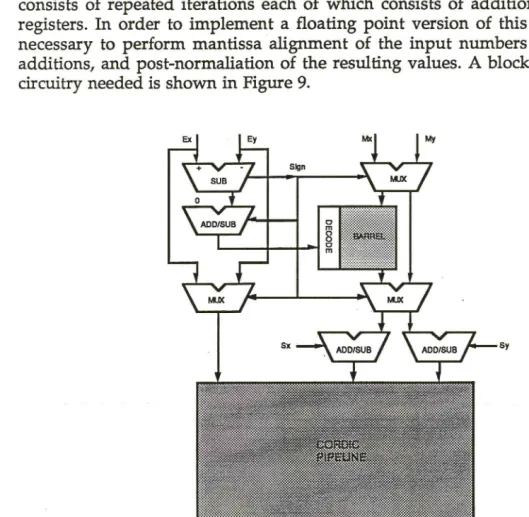
The design of the shift units for the Warwick Pipelined CORDIC processor was but a part of a larger effort aiming to produce a complete design for a pipelined realisation of the CORDIC algorithm, with the specific application of performing matrix traingularisations. The CORDIC algorithm and the design of the complete pipelined processor is described elsewhere [Chow90] and will not be repeated here. The important point to note from that work is that the algorithm consists of repeated iterations each of which consists of additions between two registers. In order to implement a floating point version of this algorithm, it is necessary to perform mantissa alignment of the input numbers to allow direct additions, and post-normaliation of the resulting values. A block diagram of the circuitry needed is shown in Figure 9.
[image:19.842.67.596.292.808.2]1Sx
Figure 9 - Block Diagram of CORDIC processor
• r-
-./-/
/
/
1,PELft•
://
1
/.„.11/N
/ /
,/
/
/ / • / ,1
/ / /
/ •
-
/ . / / - -7 -7 - •
- -/ • /
./ ,
"/ /
A
T
1-1
E.)(PONEa __DELAt
Pi
PeBarrel Shifter Design
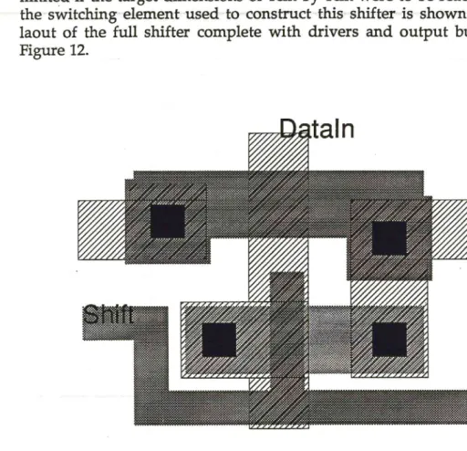
[image:20.842.74.539.85.786.2]After a number of trial layouts and simulations for the central core of a shifter with a right angle turn, it was decided that a triangular array of switching elements would be an optimal solution in order to achieve minimum spacing of the data lines. The constraint of minimal data line spacing arose from the initial designs for the main pipeline elements which indicated that the array itself would be taller than expected, and so space at the ends would become very limited if the target dimensions of 1cm by 1cm were to be reached. The layout of the switching element used to construct this shifter is shown in Figure 11. The laout of the full shifter complete with drivers and output buffers is shown in Figure 12.
[image:21.842.59.572.261.755.2]ataOut
Figure 11 - Layout of Switching Cell for Shifter
Barrel Shiffer Design
Figure 12 - Layout of Shifter using cell of Figure 11
Barrel Shiffer Design
Vdd Vdd
[image:23.842.79.563.76.269.2]Pre --I
Figure 13 - Circuit Diagram for CORDIC Shifter
When the design for this barrel shifter circuit was completed and combined with the other circuit elements making up the Pipelined CORDIC processor, it was found that the integer CORDIC pipeline was taller than had been expected, and that there was consequently less area at the ends of the array to route the data into and out of the pipeline from the Floating Point adjustment circuits. This, in conjunction with unforeseen problems with the routing of the large data busses within the floating point circuitry itself, meant that the floating point area of the chip was fairly sparse, with large areas devoted solely to routing. By redesigning the shift unit to perform the shift operation in a straight-through rather than a corner-turning topology, it is anticipated that the area wasted in this area of the chip may be considerably reduced. The design will also be able to make use of the heirarchical approach to network design described previously. The heirarchical approach to the design of the shift units was not taken originally due to the inexperience of the design team and the desire therefore to produce a straightforward working design rather than an elaborate but incorrect one.
Barrel Shifter Design
Acknowledgements
The VLSI design work was guided by Kieran Lismore who had previously worked on IC design in industry and whose support and initial instruction in the finer points of VLSI design were invaluable. He also worked on the circuitry for the generation and distribution of clock signals and provided technical and software support. The design of the major functional units for the processor was carried out by David Walton and Paul Chown. David Walton designed the main pipeline for the CORDIC iterations and Paul Chown designed the circuitry to perform the transformations between the floating point representation and the integer representation required by the pipeline. The project as a whole was coordinated by Prof. Graham Nudd who provided direction and encouragement.
References
[And67] - S.F.Anderson, J.G.Earle et al., The IBM System/360 Model 91 : Floating Point Execution Unit, IBM Journal of R & D, January 1967, pp 34-53
[Chow90] - P.M.Chown, D.W.Walton, The Warwick Pipelined CORDIC Processor, to be published.
[Henn90] - Hennessy and Patterson, Computer Architecture : A Quantitative Approach, Morgan-Kaufmann, 1990
[Mead80] - C. Mead, L. Conway, Introduction to VLSI Systems, Addison-Wesley, 1980
[Mukh86] - A.Mukherjee, Introduction to nMOS and CMOS VLSI Systems Design, Prentice-Hall, 1986
[Penf81] - P. Penfield , J. Rubenstein, Signal Delay in RC Tree Networks, Caltech Conference on VLSI, January 1981, pp 269-283
[Peng80] - V.Peng et al., On The Implementation of Shifters, Multipliers and Dividers in VLSI Floating Point Units, Proc 8th Symp. on Computer Arithmetic, May 1987, pp 95-101
[Simc86] - R.J.Simcoe, A.Fisher et al., The MicroVAX 78132 Floating Point Chip, Int. Conf. on Computer Design 1986, pp 420-425
[Vaud87] - G.J.Vaudin, Kieran Lismore, G.R.Nudd, Design and Application of a CORDIC Processor for Real-Time Signal Processing, Swansea UK IT 88 Conference, July 1988