Adaptive digital polynomial
predistortion linearisation for RF
power amplifiers
D M Giesbers
A thesis submitted in partial fulfilment of the requirements for the degree of
Master of Engineering in
Electrical and Computer Engineering at the
University of Canterbury, Christchurch, New Zealand.
CONTENTS
LIST OF FIGURES iv
LIST OF TABLES viii
ACKNOWLEDGEMENTS ix
ABSTRACT xi
GLOSSARY xv
CHAPTER 1 INTRODUCTION 1
1.1 Research objectives 2
1.2 Thesis outline 2
1.3 Contribution 2
CHAPTER 2 POWER AMPLIFIER NON-LINEARITIES 3
2.1 Non-linearity 3
2.1.1 Non-linear effects 4
2.1.2 Analysis 9
2.2 Linearisation 14
2.2.1 Feedback 15
2.2.2 Feed-forward 18
2.3 Predistortion 20
CHAPTER 3 PREDISTORTION LINEARISATION 23
3.1 Analogue 23
3.2 Analogue predistortion with digital control 27
3.3 Digital baseband predistortion 31
3.3.1 Baseband lookup table predistortion 32
3.3.2 Baseband model predistortion 35
CHAPTER 4 PA MODELLING AND DESIGN 45
4.1 Amplifier modelling 45
CHAPTER 5 SIMULATION VERIFICATION OF DESIGNED
PREDISTORTER 53
5.1 Simulation simplifications 55
5.2 Forward convergence verification 55
5.2.1 Inverse predistortion 57
5.2.2 Tracking 61
5.2.3 Quantisation 62
5.3 Performance 63
CHAPTER 6 IMPLEMENTATION 69
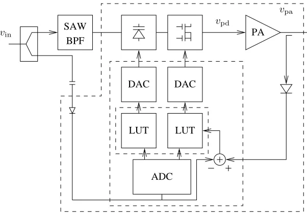
6.1 System hardware 70
6.2 Component verification 72
6.2.1 Manufacturer provided logic functionality 74
6.2.2 Sinusoid generation 75
6.2.3 Modulation and demodulation 77
6.2.4 Baseband recovery 78
6.2.5 Control 80
6.2.6 Predistortion 81
6.2.7 Adaption 83
CHAPTER 7 SYSTEM VERIFICATION AND RESULTS 87
7.1 Internal PA modelling 87
7.2 Linearisation of internal PA model 92
7.3 External PA linearisation 96
7.4 Conclusion 107
CHAPTER 8 CONCLUSIONS 113
8.1 Predistortion implementation 113
8.2 Further work 115
APPENDIX A LMS ALGORITHM 117
FIGURES
1.1 Radio architecture. 1
2.1 Non-linear circuit element with voltage source excitation. 5
2.2 Harmonic distortion spectrum. 6
2.3 Third-order IMD products with bandpass filter response. 9
2.4 Non-linear system model. 10
2.5 Simplified model of a FET, with linear and non-linear stages. 11
2.6 Frequency spectrum of the lower intermodulation frequencies produced by exciting a non-linear circuit with a two-tone signal. 13
2.7 Basic diagram of feedback linearisation. 15
2.8 Feedback linearisation at RF. 16
2.9 IF feedback linearisation circuit. 16
2.10 Cartesian feedback linearisation circuit. 17
2.11 Basic feed-forward linearisation system. 18
2.12 Predistortion linearisation in its simplest form. 21
2.13 Predistortion linearisation at IF and RF. 21
2.14 Predistortion linearisation at baseband. 22
3.1 Branch FET predistortion linearisation. 24
3.2 Third-order signal injection predistortion. 25
3.3 Third and fifth order predistortion using error amplifiers. 26
3.4 Third and fifth order predistortion using even order terms. 26
3.5 Adaptive predistortion calculated from the envelope and applied at RF. 28
3.6 RF predistortion PA system. 29
3.7 Mapping predistorter architecture. 30
3.8 Analogue baseband predistortion. 30
3.9 Digital radio baseband architecture. 31
3.11 Constant gain predistorter. 33
3.12 Cubic spline predistortion architecture. 35
3.13 Polar polynomial predistorter architecture. 37
3.14 Power series predistorter architecture. 38
3.15 Odd order polynomial predistortion architecture. 39
3.16 Volterra predistorter architecture. 40
3.17 RLS predistorter architecture. 41
3.18 Multi-layer perception predistorter architecture. 41
4.1 Setup used for measuring the amplitude and phase response of the
ZFL-2000 amplifier. 46
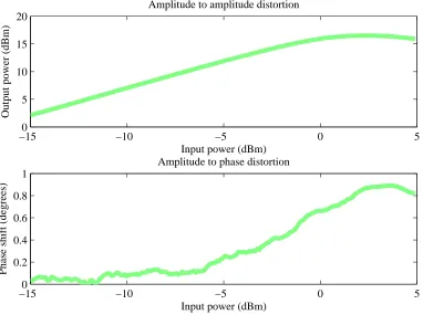
4.2 Transfer characteristics of the ZFL-2000 amplifier used in the imple-mentation of digital adaptive predistortion linearisation. 47
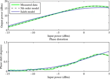
4.3 Comparison of amplifier model transfer characteristics. 48
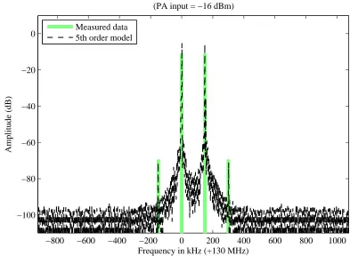
4.4 Two-tone test: -16 dBm input level. 50
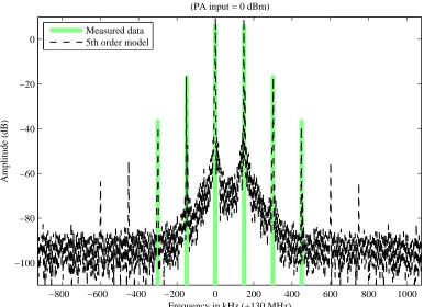
4.5 Two-tone test: 0 dBm input level. 51
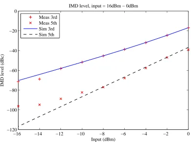
4.6 Comparison of simulated and measured IMD levels. 52
4.7 High level predistortion. 52
5.1 Standard inverse predistortion architecture. 54
5.2 Direct predistortion architecture. 54
5.3 Predistortion system architecture. 55
5.4 Simplified simulation system. 55
5.5 LMS adaptive power series configuration used to test convergence on a
forward model of the amplifier. 56
5.6 Convergence to the forward PA model coefficients from initialised values. 57
5.7 LMS Adaptive predistortion system diagram. 58
5.8 Convergence of the coefficients of an amplitude correcting adaptive
pre-distortion linearisation system. 58
5.9 PA and predistortion linearisation transfer functions. 59
5.10 AM-AM predistortion linearisation spectrum, with correction enabled
and disabled. 60
5.11 System diagram of an adaptive predistortion linearisation system to
correct for both amplitude and phase distortion. 61
5.12 Amplitude and phase transfer functions of PA and predistortion lineariser. 62
5.13 Uncorrected and corrected spectrums with amplitude and phase
FIGURES vii
5.14 Transfer functions of PA and predistorter, as the PA model
character-istic changes. 64
5.15 Predistorter coefficients changing to track a change in PA transfer
char-acteristic. 65
5.16 Linearisation of a changing PA transfer characteristic. 66
5.17 Predistortion linearisation with quantisation effects. 66
5.18 Spectrum of correction with quantisation. 67
6.1 High-level predistortion linearisation system diagram. 70
6.2 Hardware platform diagram. 71
6.3 Timing diagram showing setup and hold requirements of a typical
syn-chronous section. 73
6.4 Pipelining of combinational logic to increase clock frequency. 74
6.5 Unrolled, pipelined CORDIC. 76
6.6 CORDIC and phase accumulator. 77
6.7 Modulator/demodulator architecture. 78
6.8 Filter architecture. 79
6.9 Filter transfer functions. 79
6.10 Filters and delays used to recover the baseband signal. 80
6.11 GUI used to control the implemented predistorter. 81
6.12 Pipelined structure of the power series. 83
6.13 Verification of the power series functionality with Matlab simulation
data. 84
6.14 Structure of the LMS adaption algorithm. 85
6.15 Verification of the LMS adaption algorithm compared with Matlab
sim-ulation data. 85
7.1 System diagram of forward model LMS verification. 88
7.2 Spectrum’s of showing adaption to a forward model of the PA model on the FPGA: (a) input (b) PA output (c) LMS model output. 90
7.3 Convergence of the LMS coefficients on the FPGA over 2.7 ms. 91
7.4 Error as the coefficients converge to a forward model of the PA on the
FPGA over 2.7 ms. 91
7.5 System diagram of PD model with internal feedback LMS verification. 92
7.6 Spectrums of the PD linearistion of a PA model: (a) input (b)PA
7.7 Predistortion lineariser coefficients converging over 0.1 ms, with an
in-ternal PA model. 95
7.8 Error over 0.1 ms as coefficients of a predistortion lineariser converge,
with an internal PA model. 95
7.9 Hardware configuration and test instruments used to collect the results
in this chapter. 97
7.10 Predistortion system configuration with external PA. 97
7.11 Spectrums with -13 dBm (low power) input: (a) PA input (b) PA output. 98
7.12 Spectrum of the linearised PA output, low power input: (a) 5th order
PD (b) 7th order PD (c) Odd-only 7th order PD. 100
7.13 Spectrum with -7 dB (mid power)input: (a) PA input (b) PA output. 101
7.14 Spectrum of the linearised PA output, mid power input: (a) 5th order
PD (b) 7th order PD (c) Odd-only 7th order PD. 102
7.15 Spectrums with -3.4 dB dB (high power) input: (a) PA input (b) PA
output. 104
7.16 Spectrums of the linearised PA output, with a high power input: (a) 5th order PD (b) 7th order PD (c) Odd-only 7th order PD. 105
7.17 Fifth order coefficients and error over 0.1 ms. 108
7.18 Seventh order coefficients convergence and error over 0.1 ms. 109
7.19 Odd-only seventh order coefficient convergence and error over 0.1 ms. 110
7.20 Photo of the operating predistortion lineariser. 111
8.1 Model based predistorter architecture to correct for memory effects. 116
B.1 Architecture of a Stratix I device. 121
TABLES
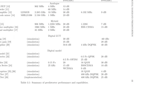
3.1 Summary of predistorter performance and capabilities. 43
4.1 Power series model coefficients fitted to the measured ZFL-2000 transfer
characteristic using least squares curve fitting. 49
4.2 IMD levels -16 dBm input power level. Note the third and fifth IMD products are below the noise floor of the measuring equipment. 49
4.3 IMD levels relative to fundamentals, with 0 dBm input power level. 49
5.1 IMD levels with AM-AM and AM-PM predistortion correction. 64
5.2 IMD levels with AM-AM and AM-PM predistortion correction. 65
6.1 Megafunctions used in the predistortion system. 75
6.2 Functions of the system controlled via RS232. 82
7.1 IMD levels of an forward LMS model of a PA model. 89
7.2 IMD levels of an internal LMS PD. 93
7.3 IMD levels of an internal LMS PD compared with simulation. 93
7.4 intermodulation levels, low power input. 99
7.5 Intermodulation levels, mid power input level. 103
ACKNOWLEDGEMENTS
ACADEMIC SUPERVISION
Dr Kim Eccleston, University of Canterbury, Christchurch, New Zealand.
TECHNICAL SUPERVISION
Dr Stephen Mann, Tait Electronics Ltd, Christchurch, New Zealand.
GENERAL ASSISTANCE
ABSTRACT
GLOSSARY
A
ACP (Adjacent ahannel power) Power level in the adjacent channel in dB.
ACPR (Adjacent channel power ratio) The ratio of power levels between a channel and its adjacent channel in dB.
ADC (Analogue to digital converter) Converts an analogue voltage level into a dig-ital signal.
C
CORDIC (Co-ordinate rotation digital computer) Iterative hardware algorithm used to compute trigonometric functions.
D
DAC (Digital to analogue converter) Converts a digital sample into an analogue voltage level.
DSP (Digital signal processor) A micro-computer designed for digital signal pro-cessing applications.
F
FPGA (Field programmable gate array) Reconfigurable hardware device.
G
I
IIR (Infinite impulse response) A filter which has an impulse response that is in-finitely long.
IMD Intermodulation distortion.
J
JTAG (Joint test action group) General purpose programming and debug stan-dard interface.
L
LAB (Logic array block) Stratix architectural block containing LEs RAM and DSP blocks.
LDMOS Lateral double diffuse metal oxide semiconductor.
LE (Logic element) Lookup table for implementing logic functionality in an FPGA.
LMS Least means squared adaption algorithm.
LO Local oscillator.
LUT (Look up table) Table mapping input value(s) to output value(s).
M
MLP (Multi-layer perceptron) Multi-layer architecture of a nueral net.
MMIC Monolithic microwave integrated circuit.
MSE Mean squared error.
MSPS Mega samples per second.
N
NN Neural net.
O
GLOSSARY xvii
P
PA (Power amplifier) Amplifies a modulated RF signal.
PLL (Phase-locked loop) Generates a clk signal that is phase locked to a reference signal.
Python An object oriented programming language.
R
RF Radio frequency.
RLS Recursive least squares.
RS232 (Recommended standard 232) Serial communications standard.
S
SFDR (Spurious free dynamic range) Level of spurious emisions produced by a de-vice.
U
UART Universal asyncronous teceiver/transmitter.
V
VHDL (VHSIC hardware description language) A hardware description language often used in the programming of FPGA devices.
VHSIC (Very high speed integrated circuits) Program initiated by the US armed forces that led to development and advance of the CMOS semiconductor industry.
Chapter 1
INTRODUCTION
Typical modern radio applications use digital hardware and digital signal processing
techniques at baseband in conjunction with analogue circuitry at radio frequency (RF)
as shown in Figure 1.1, with the trend pushing the digital to analogue interface closer
to the antenna. As more demands are placed on frequency spectrum, there is a need
for increasing the spectral efficiency of radio systems. Distortion of the RF signal
by the power amplifier (PA) is often the largest contributor to spectral inefficiency
through the increase in out-of-band signal power. The non-linear transfer function of
power amplifiers used in radio applications has been understood for some time, along
with the distortion caused to the RF signal as it is amplified. The linearisation of the
PA can be achieved using various methods in both the analogue and digital domains.
Recently, predistortion linearisation systems have been developed that operate on the
baseband signal. Many of these systems make use of an adaptive algorithm but few
systems have been implemented.
M
DAC
DAC interpolator filter
PA RF baseband
analogue digital
LO
LO I
Q
1.1 RESEARCH OBJECTIVES
The aim of this research is to design and implement a predistortion linearisation
sys-tem that operates in real time. The implemented predistortion syssys-tem is to be
inde-pendent of RF frequency, modulation format and PA transfer characteristic so must
adapt its transfer characteristic in real time. The design will be based on
topolo-gies and algorithms that have been previously designed and presented in the public
domain.
1.2 THESIS OUTLINE
The principals of non-linearity are presented in Chapter 2, along with a brief overview
of different methods of PA linearisation – feedback, feed-forward and predistortion. A
literature review of predistortion linearisation, beginning with early analogue solutions
is provided in Chapter 3. The proposed predistortion and adaption methods are used
to design the high level architecture of the implementation. The modelling of the
PA and design of the predistortion lineariser is discussed in Chapter 4. Simulation
verification of this system is presented in Chapter 5. This provides a verification
of the baseband power series predistorter topology working with an LMS adaption
algorithm to minimise the error on the RF signal. The system implementation on a
FPGA is discussed in Chapter 6. The implementation of the predistorter and adaption
algorithm is discussed, along with methods of control and data acquisition. System
verification and results are discussed in Chapter 7. The implemented predistortion
lineariser runs in real time on a hardware development platform.
1.3 CONTRIBUTION
The design and simulated performance of the adaptive polynomial predistortion
lin-earisation system has been presented at the Electronics New Zealand Conference
Chapter 2
POWER AMPLIFIER NON-LINEARITIES
This chapter provides a background to power amplifier (PA) non-linearities and how
these manifest themselves in a communications system. The traditional feedback and
feed-forward linearisation methods will be briefly discussed.
2.1 NON-LINEARITY
In order to discuss the properties and analysis of non-linear devices, non-linearity
must first be defined. To simplify discussion in this chapter, the definition of a circuit
is extended to include single elements. A linear circuit has a response that follows
the principle of superposition. Specifically, a linear combination of responses is also a
response. If a linear circuit described by
y=f(x) (2.1)
is excited individually with x1 and x2 it has responses,
y1=f(x1) (2.2)
y2 =f(x2). (2.3)
The response of the circuit when excited with a complex excitation can be found by,
f(x1+x2) =y1+y2 (2.5)
f(A·x1+B·x2) =A·y1+B·y2. (2.6)
where A, B and k are constants. This principle can be extended to cover as many
excitations as is desired.
All circuits exhibit some non-linear behaviour although adequate analysis can
often be performed under the assumption the circuit response is linear and using linear
analysis techniques. Linear analysis techniques can be used when the excitation of
the circuit is sufficiently small for that circuit to have a linear response. A circuit can
be classified as strongly non-linear, weakly non-linear, or quasi-linear, although these
categories are not formally defined. It is generally accepted that a weakly non-linear
circuit can be accurately modelled using power series analysis [2] which is described
in Section 2.1.2.
2.1.1 Non-linear effects
The most significant effects of non-linear circuits are observed as ‘frequency
genera-tion’ where frequency components not in the input are present on the output. These
phenomena are given a range of names but are often manifestations of the same
non-linear effects [2].
The following sections will examine non-linear effects common in communication
systems, in reference to Figure 2.1. Effects that limit system performance such as
harmonic distortion, intermodulation distortion and amplitude to phase conversion
will be focused on. Consider the non-linear circuit in Figure 2.1 in which the source
impedance is zero. The response of this circuit can be found easily from a Taylor
series expansion,
vout =fnl(vin) =a1vin+a2vin2 +a3vin3 (2.7)
2.1 NON-LINEARITY 5
vout
vin
fnl()
Figure 2.1: Non-linear circuit element with voltage source excitation.
Harmonic generation is one of the most common and obvious effects of a non-linear
circuit. The harmonic frequency components of an input frequency are any integer
multiples of the input frequency. Harmonic generation causes very few problems
with small bandwidth receivers, but in the case of transmitters may cause frequency
components that interfere with other systems. Consider a system described as,
vout =a1vin(t) +a2vin(t)2+a3vin(t)3+a4vin(t)4+· · ·+anvin(t)n, (2.8)
wherean are real coefficients. To simplify the analysis all coefficients of order greater
than three are set equal to zero to truncate the series,
vout =a1vin(t) +a2vin(t)2+a3vin(t)3, (2.9)
although the derivation can be shown for any number of coefficients. To investigate
the effects of harmonic distortion, consider a single tone excitation,
vin=A·cos(ωt). (2.10)
By substituting Equation 2.10 into Equation 2.9 an expression forvoutin terms of the
vout = a1Acos(ωt) +a2(Acos(ωt))2+a3(Acos(ωt))3
= a2 2 + [a1+
3 4a3A
2]A·cos(ωt) +
1 2a2A
2cos(2ωt) +
1 4a3A
3cos(3ωt). (2.11)
The response consists of a DC term and frequencies that are multiples of the input
frequency. As is evident in Figure 2.2, the unwanted frequency components introduced
by harmonic distortion can easily be removed by filters, as they are widely spaced.
dc ωin 2ω 3ω ω
A
m
pl
it
ude
Figure 2.2: Harmonic distortion spectrum.
Intermodulation is observed as frequency components that are a linear
combina-tion of two or more of the excitacombina-tion frequencies. Intermodulacombina-tion components can
pose serious problems when generated in either an amplifier or receiver as they can
interfere with or be mistaken for the desired signal [2]. Consider again the circuit in
Figure 2.1, but with a two-tone excitation,
vin=V1cos(ω1t) +V2cos(ω2t). (2.12)
By substituting Equation 2.12 into Equation 2.7 the three response terms can be
2.1 NON-LINEARITY 7
va1(t) = a1vin(t)
= a1V1cos(ω1t) +a1V2cos(ω2t) (2.13)
va2(t) = a2vin(t) 2
= 1
2a2
V12+V22+V12cos(2ω1t) +V22cos(2ω2t)
+2V1V2[cos((ω1+ω2)t) + cos((ω1−ω2)t)]
(2.14)
va3(t) = a3vin(t) 3
= 1
2a3
V13cos(3ω1t) +V23cos(3ω2t)
+3V12V2 h
cos((2ω1+ω2)t) + cos((2ω1−ω2)t) i
+3V1V22 h
cos((2ω2+ω1)t) + cos((2ω2−ω1)t) i
+3(V13+ 2V1V22)cos(ω1t) + 3(V23+ 2V1V22)cos(ω2t)
Collecting the terms gives the total response,
vout = va1+va2+va3
= 1
2a2(V
2
1 +V22) +
(a1V1+
3 2a3(V
3
1 + 2V1V22))cos(ω1t) +
(a1V2+
3 2a3(V
3
2 + 2V2V12))cos(ω2t) +
a2V1V2cos((ω1−ω2)t) +
a2V1V2cos((ω1+ω2)t) +
1 2a2V
2
1cos(2ω1t) +
1 2a2V
2
2cos(2ω2t) +
1 2a3V
3
1cos(3ω1t) +
1 2a3V
3
2cos(3ω2t) +
3 2a3V
2
1V2cos((2ω1−ω2)t) +
3 2a3V
2
1V2cos((2ω1+ω2)t) +
3 2a3V1V
2
2cos((2ω2−ω1)t) +
3 2a3V1V
2
2cos((2ω2+ω1)t). (2.16)
This power series can be evaluated to any degree of accuracy, although the analysis
quickly becomes mathematically tedious. Note also that all the generated frequencies
are a linear combination of the excitation frequencies, so the response frequencies from
a two-tone excitation will follow,
ωm,n=M ω1±N ω2 (2.17)
where M and N are real integers [2]. For ωm,n to be distinct, ω1 and ω2 must be
non-commensurate (the ratio of mixing frequencies is not a rational number). As
can be seen in Figure 2.3, the intermodulation distortion (IMD) products are close
2.1 NON-LINEARITY 9
order filter to get a transition between the passband and stopband to filter out the
intermodulation products and let the fundamental frequencies pass. Hence other
methods of removing these distortion components must be investigated.
3ω2 3ω1
2ω1+ω2 2ω2+ω1 2ω2
ω1+ω2 2ω1 ω2
ω1
2ω2−ω1 2ω1−ω2
ω2−ω1 ω
filter response realisable
A
m
pl
it
ude
dc
Figure 2.3: Third-order IMD products with bandpass filter response.
If an amplifier is driven by a large and a small signal, the large signal can drive
the amplifier into saturation. If the amplifier is driven into saturation, the gain for
the small excitation signal is also decreased. This phenomena is called desensitisation.
Saturation occurs when the coefficient of the cubic term is negative (the term does
not increase as the excitation increases).
Amplitude to phase distortion is a change in the amplitude of an excitation signal
causing a phase change on the output. This can cause large problems in a system
where the phase is important [2], such as modern modulation schemes where both
amplitude and phase carry information such as quadrature amplitude modulation
(QAM) [3][4].
2.1.2 Analysis
The process of analysing non-linear circuits is complicated by the differing degrees of
non-linearity, as different analysis techniques are more accurate for different degrees
of non-linearity. Power series analysis will be the focus of this section as it is accurate
Low frequency analysis of non-linear circuits can be performed using time-domain
analysis. Basic circuit theory can be used to derive time-domain differential equations
that describe a non-linear circuit which can be solved numerically. This method has
the following characteristics:
• Time-domain analysis can be used for lumped or distributed models.
• Frequency domain properties such as impedances are not catered for.
• It is difficult to analyse non-commensurate excitations.
Consider a weakly non-linear circuit with multiple non-commensurate small-signal
excitations. The non-linearities present typically have a negligible effect on the linear
response of the circuit. Thus we can model a non-linear system as shown in Figure 2.4.
H(w) non-linear y=f(x)
w(t) x(t) y(t)
Figure 2.4: Non-linear system model.
The transfer functionH(w) is linear, whereasf(x) is non-linear and has the form
of a power series,
y(t) =f(x(t)) =
N X
n=1
anxn. (2.18)
For practicality, the series must be restricted; values of N = 3 – 5 give results
accurate enough as the third and fifth order terms are the primary interference
com-ponents in a power amplifier. In order to apply power series analysis techniques,w(t)
and x(t) must be small-signal current or voltage, with f(x) being single valued and
weakly non-linear.
For example Figure 2.5 shows a simplified FET equivalent circuit model, with an
input linear transfer functionH(ω), whereV(ω) andVs(ω) are the frequency domain
equivalents ofv(t) and vs(t).
H(ω) = V(ω) Vs(ω)
= 1
(Rs+Ri)Cijω−LsCiω2+ 1
2.1 NON-LINEARITY 11
vs(t) Ci v(t) i=f(v) ZL(ω)
i(t) Ri
Ls Rs
Figure 2.5: Simplified model of a FET, with linear and non-linear stages.
The only non-linearity in the circuit is the transfer functioni=f(v) between gate
voltage v(t) and drain currenti(t), which can be found by power series expansion of
the large-signal drain current,
f(v) = F(Vg,0+v)−F(Vg,0)
= dF(V) dV
V=Vg,0
v+1 2
d2f(V)
dV2
V=Vg,0
v2
+1 6
d3F(V) dV3
V=Vg,0
v3+· · · (2.20)
where Vg,0 is the DC bias voltage across the capacitor.
Frequency domain analysis provides the frequency information desired. Frequency
domain analysis is also better suited to multiple non-commensurate excitations as is
common. Excitations are typically of the form,
vs(t) =
1 2 Q X q=1
Vs∗,qexp(jωqt) +Vs,qexp(jωqt)
= 1
2
Q X
q=−Q, q6=0
Vs,qexp(jωqt), (2.21)
where ω−q = −ω, Vs,−q =Vs∗,q and H(ω−q) =H∗(ωq). This assumes no DC
compo-nent which is normal for microwave excitations. Nonlinearities can produce DC
com-ponents, however, this is rarely the case with small-signal driven weakly non-linear
circuits [2] which are of importance here. Given the excitation of Equation 2.21, the
v(t) = 1 2
Q X
q=−Q
Vs,qH(ωq)exp(jωqt) (2.22)
By substituting Equation 2.22 into Equation 2.18 and solving foranvn(t) the entire
responsei(t) can be found,
i(t) =
N X
n=1
anvn(t). (2.23)
where
anvn(t) = an
1 2
Q X
q=−Q
Vs,qH(ωqt) n
= an 2n
Q X
q1=−Q
Q X
q2=−Q
· · ·
Q X
qn=−Q
Vs,q1Vs,q2· · ·Vs,qnH(ωq1)H(ωq2)· · ·H(ωqn)
exp[j(ωq1+ωq2+· · ·ωqn)t] (2.24)
It is evident that a large number of new frequencies are generated by the
non-linearities, withnth degree terms and Qexcitation frequencies. The total response of
the system is the sum of all possible linear combinations ofQexcitation frequencies.
Some of the lower order intermodulation terms are shown in Figure 2.6.
An nth order mixing frequency is one that arises from the sum of n excitation
frequencies. The situation of most concern during system design is a two-tone
exci-tation (Q = 2) and N ≤ 3 [2]. It is impossible to determine the order of a mixing
product from its frequency, as the particular frequency may be obtained from many
mixing frequencies as shown in Equation 2.25
2ω1−ω2 = ω1+ω1+ω2(3rd)
2.1 NON-LINEARITY 13
3ω2 3ω1
2ω1+ω2 2ω2+ω1 2ω2
ω1+ω2 2ω1 ω2
ω1
2ω2−ω1
ω ω2−ω1
A
m
pl
it
ude
2ω1−ω2 dc
Figure 2.6: Frequency spectrum of the lower intermodulation frequencies produced by exciting a non-linear circuit with a two-tone signal.
To demonstrate power series analysis, consider a two-tone excitation. The second
order component of the response i2(t) can be found,
i2(t) = a2v2(t)
= a2 4
2 X
q1=−2
2 X
q2=−1
Vs,q1Vs,q2H(ωq1)H(ωq2)·exp[j(ωq1+ωq2)t]. (2.26)
These terms include harmonics of the input frequencies, repeated terms and DC terms
as well as intermodulation terms. All the terms appear in complex conjugate pairs
and can therefore be expressed as shown forω1−ω2,
i′2(t) = a2v2(t)
ω1−ω2
= a2|Vs,1Vs,2H(ω1)H(ω2)|cos[(ω1−ω2)t]. (2.27)
i3(t) = a3v3(t)
= a3 8
2 X
q1=−2
2 X
q2=−2
2 X
q3=−2
Vs,q1Vs,q2Vs,q3H(ωq1)H(ωq2)H(ωq3)
·exp[j(ωq1+ωq2ωq3)t] (2.28)
This summation has (2Q)n = 43 = 64 terms, although as in the case ofi
2(t) these
do not all represent different mixing frequencies. Each of these mixing frequencies can
also be expressed in a cosine form as shown for 2ω2−ω1:
i′3(t) = a3v3(t)
2ω2−ω1
= 3a3 4
Vs,1Vs2,2H(ω1)H2(ω2)
cos[(ω2−ω1)t] (2.29)
Volterra series is similar to power series analysis, but also caters for analysis of
phase distortion.
2.2 LINEARISATION
Frequency governing bodies stipulate the power levels that can be transmitted into the
unlicensed spectrum. With non-linear effects as previously discussed causing spectral
emissions at frequencies that are not present on the input, this poses a problem for
ra-dio communication devices. As in Figure 2.6, the two main areas of spectral emissions
are at the harmonics of the input frequencies and at the intermodulation frequencies.
Filtering can be used to reduce the harmonic emissions to acceptable levels, but are
not plausible to remove the intermodulation emissions. A number of methods to
re-duce these emissions by way of linearising the PA are used for this purpose, such as
feedback or feed-forward linearisation, which are discussed in detail in the following
sections. The main restriction imposed by feed-forward linearisation for
2.2 LINEARISATION 15
operating in the linear region, however, to increase the power efficiency they are often
driven nearer the saturation region. Predistortion linearisation is discussed further in
the following chapter.
2.2.1 Feedback
As the name suggests, feedback linearisation is achieved by feeding the output signal
back into the input. This can be implemented in a range of ways, the most basic idea
of which is shown in Figure 2.7. More complex variations of feedback linearisation use
the feedback signal in different ways, such as in IF and baseband feedback linearisation
schemes as discussed in this section.
PA summer
input output
Figure 2.7: Basic diagram of feedback linearisation.
Feedback linearisation schemes correct for non-linearities over a narrow bandwidth
because a bandpass filter is used to limit the bandwidth of the loop to maintain loop
stability [3]. For stable loop operation the gain of the loop must be less than one
at any point of operation where the phase margin is exceeded, which is controlled
by the bandpass filter [3]. As any delay causes a phase shift, the total delay in the
loop must also be small enough to ensure against instability due to phase margin
violation. Over time, different methods of feedback linearisation have been developed
to simplify implementation and increase performance. The basic distinction between
implementations is the stage filtering and summing takes place (RF, IF or baseband).
The most simple feedback linearisation scheme when inspected as a full system
is shown in Figure 2.8. Difficulties arise, however, as filters and amplifiers are more
difficult to design at higher RF frequencies [3]. The filters used in RF feedback
linearisation are typically cavity resonators, which only operate at a fixed frequency
system, regardless of whether it is implemented at RF, IF or baseband. The stability of
the system is affected by the loop delay and the open loop gain. Feedback linearisation
is like all feedback systems in that instability results from violating the gain or phase
margins. As the overall gain margin must be preserved, a feedback linearisation
system uses a bandpass filter to allow high gain over the bandwidth which requires
linearisation and low gain for the remainder of the bandwidth of the system. This
means that there is a trade off between bandwidth and gain to maintain the overall
open loop gain margin.
RF out band pass
filter PA
attenuation phase
correction summer
RF in
Figure 2.8: Feedback linearisation at RF.
The primary motivation to implement feedback linearisation at an intermediate
frequency is to simplify the filter design [3]. Figure 2.9 shows an IF feedback circuit
diagram. Note that the circuit is more complicated than the RF circuit in Figure 2.8
requiring mixers, additional filters and amplifiers. The phase shift no longer needs to
be implemented in the feedback path, as a phase shift of the last mixer has the same
effect.
phase shift
amplifier IF
SSB
PA RF out
attenuation band pass
filter RF in
local oscillator
Figure 2.9: IF feedback linearisation circuit.
perfor-2.2 LINEARISATION 17
mance than single resonator cavities [3]. The up-converter must be a single side-band
mixer, as the unwanted side-band causes distortion through the power amplifier [3].
Additional filtering of the output of the power amplifier is also required to reduce the
effects of the LO and unwanted side-band [3].
Baseband feedback seeks to simplify the filtering requirements even further than
IF feedback by fully demodulating the signal and implementing the feedback summer
and filters at baseband. The main form of baseband feedback linearisation is Cartesian
loop feedback, as shown in Figure 2.10, and has been evaluated for both narrow
band-width systems (10 k symbols/s) and wide bandband-width systems (500 k symbols/s) [6]
as discussed later in this section.
loop RF Out
phase PA
oscillator filter
local
adjust
π/2 π/2
Figure 2.10: Cartesian feedback linearisation circuit.
Feedback systems were originally designed with the feedback summing and
fil-tering all done in analogue at RF, IF or baseband. As the development of digital
signal processor (DSP) devices, analogue to digital converters and digital to analogue
converters progresses, there is also a progression to digitally implement as much of
the loop as possible. In the case of Cartesian feedback loops this removes the need
for quadrature modulators and demodulators, as these can be implemented digitally
and mixed up to RF from an digitally generated IF [7].
Feedback linearisation can offer up to 35 dB correction, with a 60% power
however can only be applied to a narrow bandwidth system (less then 1 MHz
lin-earised bandwidth). Correction in the order of 35 dB can only be expected from the
complicated baseband correction schemes, with IF systems providing around 30 dB
correction and RF feedback providing as little as 10 dB IMD correction [8].
2.2.2 Feed-forward
Much of the effect of non-linearities in a power amplifier are observed as third
or-der intermodulation on the output. Feed-forward linearisation seeks to cancel the
intermodulation distortion by creating a distortion signal with an auxiliary amplifier,
to cancel the distortion produced in the power amplifier. Figure 2.11 shows a block
diagram of a feed-forward linearisation system. Note that the forward loop has two
parts. The input signal is split into two paths, one through the main PA and the other
through a delay element with a delay equal to the delay through the PA. The signal at
the output of the main PA has both the amplified signal and distortion components.
The signal component is cancelled by the delayed version of the input at couplerC3
leaving only the distortion components. These components are amplified through the
auxiliary amplifier and used to cancel the distortion components of the output of the
main PA at couplerC4.
RF in
PA
RF out
delay
delay
aux
C1 C2
C3
C4
Figure 2.11: Basic feed-forward linearisation system.
As discussed in Section 2.2.1, feedback linearisation is only stable over narrow
bandwidths which limits its use in high bandwidth applications. Feedfoward
lineari-sation, however, is unconditionally stable [9] leading to high bandwidth correction
capabilities. Successful linearisation through the removal of distortion components
2.2 LINEARISATION 19
the system. To achieve a 30dB cancellation, the amplitudes must be matched within
0.22dB and the phases must be matched to within 1.2o [8].
Feed-forward linearisation requires two amplifiers, lowering the power efficiency.
The most important design consideration for feed-forward linearisation systems is
the two delay components. For optimal linearisation, these delays must be exactly
the same as the delay through the amplifiers to ensure the distortion component
cancels the signal at the correct point in time. The couplers are also an important
design consideration. Couplers are used to both sample and sum signals throughout
feed-forward linearisation. As couplers are typically constructed using 14 wavelength
strip-line, they must be designed for the frequency band in use.
Design of the auxiliary amplifier is also an important consideration. The gain of
this amplifier is substantially lower than the power amplifier, but care must be taken
that the signal does not further distorted through this amplifier. As the delay elements
are critical to the performance of feed-forward linearisation systems, they have been
the focus of much research. Performance can be improved by replacing the typical
linear delay elements with phase distorting elements that match the phase distortion
characteristics of the amplifiers. This approach increases both the bandwidth of the
system and correction levels [10].
Distortion correction of around 25 dB – 30 dB can typically be achieved in
manu-factured equipment, with the limiting factor nearly always being the bandwidth over
which a given accuracy can be achieved [8].
The outputs from the main amplifier and error amplifiers are typically combined
using couplers that maximise power transfer from the main amplifier. A 10 dB
cou-pling ratio is often used, so 90% of the power from the main amplifier reaches the load.
However this means that only 10% of the power from the auxiliary amplifier reaches
the load, so 10 times the distortion in the main amplifier must be produced. As a
result, the auxiliary amplifier can consume a significant amount of power. Additional
to this, it may be necessary to operate both amplifiers well into back-off to improve
to 10% - 15% [8].
2.3 PREDISTORTION
This section provides a brief explanation of predistortion linearisation, which is further
discussed in the following chapter. Predistortion linearisation in its simplest form
involves distorting the signal prior to amplification in the inverse manner to which
the power amplifier will distort the signal [8]. The outputvpa of the power amplifier
will be a non-linear function of its input vin. Consider the predistortion lineariser
with an excitation signal in Figure 2.12. The output of the power amplifier will be a
non-linear function of the input,
vpa =fnl(vpd). (2.30)
Conversely, if the input signal is distorted with a non-linear function prior to
ampli-fication, then the output is a non-linear function of that distorted signal,
vpd=gnl(vin), (2.31)
where vpd is a non-linear function of the predistorter input vin. The predistorter is
designed such that
vpa = fnl[gnl(vin)]
fnl[gnl(vin)] =k·vin,
(2.32)
wherekis a constant.
As discussed in Chapter 2, the AM-AM distortion and AM-PM are significant in
typical PAs. The AM-AM characteristic is determined by the saturation level of the
2.3 PREDISTORTION 21
gnl fnl
vin vpd vpa
Figure 2.12: Predistortion linearisation in its simplest form.
The AM-PM characteristic is caused by a changing phase shift of a signal through the
amplifier, which is also a function of the input power level. Memory effects can also
cause distortion. Predistortion linearisation has the potential for excellent wideband
performance [11] and can be implemented a number of different ways, using either
analogue or digital circuitry and at both RF, IF and baseband [8].
Early predistortion linearisation techniques were based around an analogue
dis-tortion or signal injection. Methods of injecting third-order and fifth order
intermod-ulation products with a single distortion element were found to be less effective than
individual generation. This performance gain, however, comes at the cost of a more
complex system [12]. A higher level of linearisation is possible using digital systems to
control either analogue or digitally generated IM products. Further performance
im-provements are realised when predistortion is applied to the complex baseband signal,
with the PA output attenuated and demodulated to use in adapting the predistorter’s
transfer characteristic. As is the case with previously discussed linearisation
meth-ods, the more complicated schemes provide superior correction, with adaptive digital
predistortion out-performing analogue implementations.
Predistortion linearisation at RF or IF, as shown in Figure 2.13 is the most
simplistic configuration, with a non-linear element placed before the amplifier. A
system of this configuration is limited to analogue implementation, as digital signal
processing can not be performed fast enough to manipulate an RF signal.
PA PD
RF or IF
Figure 2.13: Predistortion linearisation at IF and RF.
to the complexity of the system and the level of correction required. A small level of
correction can easily be obtained by use of analogue distortion at RF, whereas more
correction can be realised with a complex adaptive algorithm at baseband using a full
demodulation of the PA output signal for adaption. Predistortion is explored in detail
in Chapter 3.
PD Q
PA LO
LO I
Chapter 3
PREDISTORTION LINEARISATION
In this chapter the theory of predistortion linearisation is presented along with the
technology progression from earlier analogue implementations through to digital
base-band systems. As discussed in Chapter 2, the traditional approaches to
linearisa-tion have disadvantages of low bandwidth (feedback) or low power efficiency
(feed-forward), both of which are undesirable for modern communication systems.
Predis-tortion linearisation provides a higher bandwidth, higher power efficiency linearisation
option.
3.1 ANALOGUE
Analogue predistortion is typically performed at radio frequency (RF). As with
feed-forward predistortion, the bandwidth of the system is limited by the consistency of
gain and phase of an analogue predistorter over the operational bandwidth.
Addi-tional limitations are from memory effects in the power amplifier (PA). Analogue
predistortion linearisation demonstrates the potential of this technology but quickly
becomes a complex system. Independent non-linear analogue elements can be used
to provide a number of fixed predistortion characteristics that are difficult to adjust.
Each of the independent predistortion characteristics must then be combined to form
the complete predistortion characteristic. This means each analogue RF predistorter
must be designed for a specific PA and its operating conditions. As in the case of
feed-forward linearisation, performance is often limited by the gain and phase flatness
linearisation architecture does not inherently require a second amplifier and thus is
able to provide higher power efficiency.
Different methods of predistortion all generate intermodulation products from
the input signal and then combine this distorted signal with the input to produce
the predistorted input to the PA. As with feed-forward linearisation, matching the
phase of the two signal paths increases the system complexity. To overcome this,
a branch FET can be used to directly distort the input signal of the PA, providing
third-order linearisation [13]. This method of predistortion as shown in Figure 3.1
does not require phase matching circuitry. A two-tone test with tone separation of
4 MHz at 902 MHz shows an reduction in third-order intermodulation products by
13 dB. This predistortion could be implemented in a monolithic microwave integrated
circuit (MMIC).
FET1
FET2
PA
vctrl Rs
vin
vpd vpa
Figure 3.1: Branch FET predistortion linearisation.
An analogue third-order signal injection predistorter for use in CDMA systems [11]
is shown in Figure 3.2. The fixed third-order product is generated by a cubic
non-linearity and combined into the main RF path, delayed to match the phase of the two
parallel paths. In a two-tone test an 18 dB reduction in the third-order
intermod-ulation is achieved, however, the performance is limited by the unwanted additional
higher order intermodulation products produced by the predistorter. Fifth order
inter-modulation products are 4 dB higher than the third-order so the total interinter-modulation
improvement is 14 dB. This architecture allows for bandwidths of up to 60 MHz, with
3.1 ANALOGUE 25
A
PA
3rd order NL
amplitude and phase control att
buffer
buffer τ
vin
()3 Φ
vpd
vpa
Figure 3.2: Third-order signal injection predistortion.
A more complex intermodulation generation system shown in Figure 3.3 as
pro-posed in [12] demonstrates an increase in linearisation performance. The system uses
independent amplifiers to produce third and fifth order distortion products which are
phase adjusted and combined with the fundamental. The PA used is a two stage
lateral double diffuse metal oxide semiconductor (LDMOS) class AB amplifier with
a 450 W peak power output. The third and fifth order intermodulation phases vary
relative to each other over the input power range, so independent phase control of
the third and fifth order linearisation products is required. The complexity of the two
stage amplifier also makes it difficult to match the non-linear characteristics of the
predistorter and the PA because they differ both in size and the number of stages.
Experimental results with a 10 MHz spacing two-tone signal at 2.385 GHz reduces
the intermodulation products by 30-35 dB. When used in combination with a CDMA
signal with 8.192 MHz bandwidth, the adjacent channel power (ACP) is reduced by
9 dB [12].
An alternative to using error generation amplifiers is to generate the
intermodu-lation products by generating even order terms and using these even order terms to
generate odd order terms. The system shown in Figure 3.4 uses I/Q balanced
mod-ulators and double balanced ring diode mixers as intermodulation generators [14].
The low frequency second order intermodulation component (ω2 −ω1) is generated
with a non-linear power amplifier, with the fourth order intermodulation (2ω2−2ω1)
intermod-cancellation
delay
IMD control error
generation
signal
PA
vin vpd vpa
Figure 3.3: Third and fifth order predistortion using error amplifiers.
ulation components are generated and phase adjusted, before being combined with
the RF signal. As with error amplifiers, the intermodulation product amplitude and
phase can both be independently controlled. Experimental results using an MHL21336
35 dBm PA from Motorola, with a 1 MHz spacing two-tone test at 2.150 GHz shows
a 23 dB reduction in third-order intermodulation and 10 dB reduction in fifth order
intermodulation [14].
delay delay
phase adjust
diode mixers PA
vin vpd
Φ Φ
vpa
3.2 ANALOGUE PREDISTORTION WITH DIGITAL CONTROL 27
3.2 ANALOGUE PREDISTORTION WITH DIGITAL CONTROL
To provide more correction to third and higher order intermodulation products,
dig-ital methods of predistortion have been investigated. Initial digdig-ital predistortion
al-gorithms used look up tables (LUTs) to map an input signal to a predistorter output
signal [15][16]. As with all predistortion linearisation systems, the predistorter output
drives the input of the PA. With digital predistortion came adaptive capability, which
allows the predistortion characteristic to be adjusted to improve the intermodulation
reductions. Adaptive predistortion also means that a general predistortion system can
be used with different amplifiers and configurations, which exhibit different distortion
characteristics.
As identified in the previous section, there is a need to control the generation
of different intermodulation products for predistortion linearisation independently,
as they are independent functions of the input signal. It is also known that not
only do different PAs have different transfer functions but that the transfer function
of an amplifier will vary over its range of operating frequencies and environmental
conditions. An extension to fixed analogue predistortion is to provide a method
by which the predistortion transfer function can adapt in real time to linearise an
amplifier operating under different and changing conditions causing the PA’s transfer
characteristic to vary. This section will investigate the addition of digital adaption
algorithms to analogue predistorters.
The general architecture of a digitally adapted analogue predistorter is shown in
Figure 3.5. The predistortion is performed at RF, with detectors to provide
informa-tion for a digital adapinforma-tion algorithm. This sort of architecture means that the system
must be designed around the characteristics of the modulated RF signal. Typically
the adaption is calculated from the envelope of the input signal and the amplified
pre-distorted signal envelope, as these signals are at low enough frequencies to perform
operations on digitally.
The wide range of digital predistorters available vary in both intermodulation
predistortion
adaption
PA
vpa vpd
vin
Figure 3.5: Adaptive predistortion calculated from the envelope and applied at RF.
A predistorter which is integrated onto an monolithic microwave integrated circuit
(MMIC) that also contains a PA is shown in Figure 3.6 [15]. The input to the module
is filtered and then passes through a phase shifter and a variable gain block. A dual
gate FET is used for the gain controlling block with the gain easily being controlled by
varying the voltage on its second gate. This causes a phase shift on the output of the
gain controlling block which must also be corrected by the phase shifter. The phase
and gain of the predistorter are controlled with analogue control signals derived from
lookup tables (LUTs) addressed by the input envelope level. The contents of the two
lookup tables are updated by an algorithm that compares the input envelope with the
PA’s output envelope. This module has been designed for CDMA handset terminals
and therefore has a bandwidth of 1.2288 MHz and a centre frequency of 906 MHz.
Two-tone tests demonstrate a reduction in the third-order intermodulation products
of 20 dB when tested with an N-CDMA signal, adjacent channel power (ACP) is
reduced by 7 dB [15].
Increasing the characteristic information available to a digital/RF predistorter as
presented in [16] further increases the linearisation capabilities. In the system shown in
Figure 3.7, the lookup table is able to better reproduce the predistortion characteristic
as it is a two dimension lookup table, with non-uniform input quantisation. This is
known as mapping predistortion, as the lookup table maps the input envelope to
I and Q correction vectors. The input RF signal envelope is detected and used to
find I and Q vectors which are multiplied onto the RF input to the PA. As the I
and Q are predistorted with independent lookup tables, the input to the PA and
3.2 ANALOGUE PREDISTORTION WITH DIGITAL CONTROL 29
PA SAW
BPF
LUT DAC
ADC LUT DAC
vpa
vin
[image:47.595.164.465.111.323.2]vpd
Figure 3.6: RF predistortion PA system.
algorithm to adjust the lookup table contents. The lookup table predistortion is
implemented in an FPGA with adaption performed by a DSP. This method again
requires precise phase matching of the RF signal and the output from the lookup
table. A two-tone test with tone separation of 1 MHz at 1960 MHz demonstrates
a reduction of the third-order intermodulation by 20 dB. With a CDMA IS95 input
signal, third-order intermodulation is reduced by 15 dB. When compared with complex
gain predistortion, the two-tone performance is similar, however, the adjacent channel
power of a CDMA signal is reduced a further 8 dB by the more complex mapping
predistorter [16].
When predistortion is applied at RF, the predistortion system must be designed
specifically for the bandwidth and frequency of the modulated RF signal. In order
to design a predistortion system that operates independent of the RF signal
charac-teristics, the predistortion must be applied at baseband. As baseband processing is
typically done digitally in modern communications systems, there is a trend towards
digital implementation of baseband predistortion as discussed in Section 3.3. The
lin-earisation shown in Figure 3.8 demonstrated a digitally adapted analogue predistorter
operating at baseband [17]. The complex baseband I and Q signals are predistorted
LPF
ADC
RX DSP
LUT
LPF DAC LPF
PA vin
vpd
vpa
LO
[image:48.595.187.367.570.731.2]FPGA
Figure 3.7: Mapping predistorter architecture.
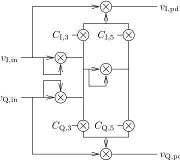
vI,pd = vI1,in+CI,3vI3,in+CI,5v5Q,in (3.1)
vQ,pd = vQ1,in+CQ,3vQ3,in+CQ,5vQ5,in (3.2)
The coefficients are calculated using the Hooke and Jeeve algorithm which uses the
side-band power as the minimisation criterion. This system reduces third-order
inter-modulation by 20 dB with a 2 MHz tone separation at 35 MHz [17].
vQ,in vI,in
CI,3 CI,5
CQ,3 CQ,5
vQ,pd vI,pd
3.3 DIGITAL BASEBAND PREDISTORTION 31
3.3 DIGITAL BASEBAND PREDISTORTION
This section outlines the basics of complex baseband manipulation before discussing
predistortion linearisation methods that operate on the baseband signal.
A typical digital radio system has the architecture shown in Figure 3.9. A digital
bit stream is modulated onto a complex baseband signal with in-phase (I) and
quadra-ture (Q) components. For any given modulation format a binary word of length N
bits is mapped onto a symbol on the complex plane, such that each binary word has
a unique symbol. The complex baseband is then up-sampled and filtered to limit the
bandwidth of the signal before being modulated onto an RF carrier. Each symbol of
the complex baseband corresponds to an amplitude and phase of the RF signal as
RF =Q·cos(ωct) +I ·sin(ωct) (3.3)
As this process of quadrature modulation can be reversed to recover the I and Q, it
follows that predistortion of the complex baseband signal can linearise the non-linear
transfer characteristic of the PA operating at RF.
"1101" RF
M vQ,in
sin(wct)
cos(wct) vI,in
Figure 3.9: Digital radio baseband architecture.
The process of digital baseband predistortion can be divided into two main
cate-gories:
• LUT-based
• Model based
Lookup table based methods use a lookup table to find a distorted output based on
predistortion characteristic. Model based predistorters calculate a pre-distorted
out-put from a mathematical model of the predistortion transfer characteristic. Adjusting
the model parameters adapts the transfer characteristic of the predistortion to
min-imise an error criterion. In the following section lookup table based predistortion is
discussed, followed by discussion of model-based predistortion.
3.3.1 Baseband lookup table predistortion
This section will look at examples of lookup table predistorters which can be divided
into two categories:
• Complex gain predistortion
• Mapping predistortion
As its name suggests, a mapping predistorter maps a pure input signal to a distorted
output signal. A complex gain predistorter, however, uses a function of the input
signal (often the input power) to index the output distorted signal level.
The pioneering research into digital baseband predistortion employs a mapping
LUT architecture [18] shown in Figure 3.10. The complex baseband signalvinis used
to index a two dimensional lookup table. The output of the lookup table is added tovin
to find the predistorted complex baseband signal vpd. This is converted to analogue,
quadrature modulated and up-converted to RF before being amplified. The output of
the PA is down-converted and demodulated to recover the complex baseband which
in turn is used to adapt the contents of the lookup table. This architecture is capable
of reducing the out-of-band power of a QPSK channel to -60 dBc – a 30 dB reduction
to the third-order intermodulation. The time this predistorter takes to converge to a
steady state is slow – around 5-10 seconds, due to the large memory contents to be
updated.
A constant-gain predistorter [19] is shown in Figure 3.11. The instantaneous
power of the complex baseband signal is calculated and used as an input to a single
3.3 DIGITAL BASEBAND PREDISTORTION 33
RAM
PA DAC
delay
ADC updating circuit
∆θ
delay adjust vI,in
vQ,in
vpd
vpa
Figure 3.10: Mapping predistorter.
the predistorted complex baseband signal. In an implementation of a complex gain
predistorter, vpd would be converted to analogue complex baseband and modulated
onto an RF carrier. In simulation results this system is capable of reducing up to
15th order intermodulation products. The third-order intermodulation of this system
is reduced by 55 dB to -75 dBc, however, the seventh order intermodulation raises
the out-of-band power to -65 dBc. When simulating the linearisation of a 16 QAM
channel, the third-order intermodulation is reduced to -60 dBc from -32 dBc. This
predistorter linearises up to 95% of a PA’s saturated power output level. Convergence
to a steady state takes 4 ms, a significant reduction from 5-10 seconds for a mapping
predistorter.
DAC
ADC
PA
adjust
| · |2
LUT vQ,in
vI,in vpa
vpd
Further developments into the area of LUT-based baseband predistortion have
been in the refinement of the way the LUT is stored and adapted. One such method
as shown in Figure 3.12 uses cubic spline interpolation to populate a complex gain
predistorter LUT [20]. The instantaneous power of the complex baseband is calculated
and used as an input to an LUT, the output of which is added to the complex baseband
I and Q samples. The LUT table contents is updated by an AM-AM and AM-PM
estimator which compares the pre-distorted complex baseband with the demodulated
output of the PA. This estimator calculates r, r′ and θ′ values using cubic spline
interpolation,
r = qvI2,in+v2Q,in (3.4)
r′ = qv2
Q′ +vQ2′ (3.5)
θ′ = tan−1(vQ′ vi′
), (3.6)
where for an input to the LUTm, the updated values of the amplitude characteristic
m′ and phase characteristicφ′ are calculated. Thus the predistorted signal is the sum
of the LUT output and the complex baseband signal,
vI,pd = vI,in+r′·cosθ′ (3.7)
vQ,pd = vQ,in+r′·sinθ′. (3.8)
This system performance is analysed using simulation of a class AB PA
charac-teristic with both two-tone and DQPSK input signals. With a two-tone at 22.25 kHz,
third-order and fifth order intermodulation are reduced to -80.3 dBc and -81.2 dBc
respectively from -29.6 dBc and -38.1 dB respectively. With a 40 kHz DQPSK channel
3.3 DIGITAL BASEBAND PREDISTORTION 35
LUT delay vpd
ADC
DAC PA
|·|2
vI,in
AM-AM & AM-PM estimator vQ,in
vpa
Figure 3.12: Cubic spline predistortion architecture.
3.3.2 Baseband model predistortion
Further improvement in the correction capability of predistortion systems are
pro-vided by using a mathematical model of the predistortion function. These systems
use a predistorter that can calculate the required predistortion characteristic from
a small number of model parameters. The model parameters can be adapted more
quickly than the contents of an LUT, but more computation is required to apply the
predistortion. Due to limitations of micro-processor based DSPs, this type of
predis-tortion can only be implemented at baseband, or a low intermediate frequency. Much
of the research into this area has been on one of two main thrusts:
• Increasing predistorter performance with more accurate and complex models
• Refining the process used to adapt model parameters to reduce convergence
times
The expected results from this research have been extensively simulated, however,
many of the approaches have not been implemented in real-time operational systems.
The predistortion system shown in Figure 3.13 applies a predistortion
character-istic to the complex baseband signal in polar co-ordinate format [21]. As described
in Chapter 2 the distortion characteristics of a typical PA have independent AM-AM
and AM-PM functions. This makes application of a predistortion straightforward, as
shown in Figure 3.13. The AM-AM and AM-PM predistortion functions are modelled
|vpd| = vin· N X
i=0
αiρ2i, (3.9)
∠vpd = vin· M X
i=0
βiρ2i. (3.10)
In this case,iis chosen as 2. Input complex baseband signal instantaneous power
ρ2xis calculated and used as an input to the independent amplitude and phase
polyno-mials. The output from the amplitude and phase polynomials are multiplied with the
complex baseband signals after being converted back into rectangular co-ordinates to
realise the predistorted complex baseband signal. The coefficients of the polynomials
are updated by minimizing the following cost function,
C2= N X
i=1
w(ρ2)[A(ρ2)−AN(ρ2)]2. (3.11)
where A is the AM-AM transfer function. With a 256 QAM signal, this method
reports a further 5.2 dB decrease in out-of-band power compared with a popular
third-order predistorter with transfer function,
vpd =f(at+btρ2) (3.12)
when compared with a popular fifth order predistorter with transfer function, an
additional 2 dB reduction of out-of-band power is obtained,
vpd =f(at+btρ2+ctρ4). (3.13)
An alternative to using independent polynomials for AM-AM and AM-PM
pre-distortion is to have a polynomial predistorter with complex coefficients [22]. As is
shown in Figure 3.14, the complex baseband signal is distorted through a polynomial
predistorter before being converted into analogue signals, modulated and then
3.3 DIGITAL BASEBAND PREDISTORTION 37
| · |2
e−j(.) θ(.)
A(.)
converter
vin vpd
polar to rectangle ρ2
Figure 3.13: Polar polynomial predistorter architecture.
sampled into a digital complex baseband. The LMS algorithm is used to adapt the
coefficients of the predistorter by minimising the error between the complex baseband
signal and the complex feedback from the PA output as
f(n) =f(n−1)−µ· ▽J(n), (3.14)
where f(n) is the vector of the polynomial coefficients and ▽J(n) is the gradient of
the error vin−vpa.
Simulations [22] of this predistortion system use a 9th order polynomial model of
the transfer characteristic of a class AB MOSFET amplifier and a third-order
predis-torter 3.14. When a QPSK modulation format is used, with a bandwidth of 0.5 Fs,
the channel power is reduced by 4 dB and third-order intermodulation is reduced by
20 dB. The reduction in the output power of the PA also reduces the fifth, seventh
and ninth intermodulation products by 8 dB. With an orthogonal frequency division
modulation (OFDM) format, the channel power is reduced by 5 dB and third-order
intermodulation is reduced by 25 dB, with fifth, seventh and ninth intermodulation
products all being reduced by 15 dB due to the lower power output of the PA.
Figure 3.15 shows a model based predistortion lineariser using independent
AM-AM and AM-AM-PM polynomials with odd order coefficients only [23]. The predistorted
signal is a function of the amplitude of the complex baseband signalr(t),
vpd(t) =F(r(t))ej(θ(t)+Ψ(rin(t))), (3.15)
LUT PD
vpd
DAC
ADC
vpa
vQ,in
PA vI,in
Figure 3.14: Power series predistorter architecture.
The amplitude of the input complex envelope is calculated and used as an input
to the two predistortion functions. The AM-AM distortion is applied by multiplying
the calculated distortion with the complex baseband. AM-PM distortion is applied
using a LUT to get values of cos and sin for a rotation matrix. The transfer functions
of the two predistortion functions are adapted by minimising the mean squared error
criteria,
JAM−AM = E((αr−G(VTRf))2) (3.16)
JAM−PM = E((Φ(VoptT Rf) +PTRphi)2). (3.17)
With coefficients being updated using,
Vk+1 = Vk+µvΓfRf,kα−G(Vk|TRf,k) (3.18)
Pk+1 = Pk−µφ(Φ(VkTRf,k) +PkTRφ,k)ΓphiRphi,k, (3.19)
whereα is the desired linear gain, Γx= q
E(Rx,kRxT,k) and both µv and µφ are step
sizes.
In simulated two-tone tests with a tone separation of 0.15Fs the intermodulation
is lowered to -60 dBc compared with -40 dBc intermodulation with no predistortion
3.3 DIGITAL BASEBAND PREDISTORTION 39
by 30 dB.
vpa PA
F vr,in
DAC vI,pd
vQ,pd
r(t)
Ψ θ
I θ Q r
Figure 3.15: Odd order polynomial predistortion architecture.
Minimisation of the distortion caused by PA memory effects can be achieved
with a Volterra series predistorter. This transfer characteristic allows correction of
AM-AM, AM-PM and memory effect distortion [24]. As shown in Figure 3.16, the
complex baseband signal is predistorted with an adaptive Volterra filter. The adaption
is applied using a direct inversion, where the output of the PA is iteratively adapted
to find the predistortion coefficients which are copied to the predistorter model. The
Volterra filter coefficient vector has third-order terms, with a delay line of 2 samples
to allow for cancellation of the distortion caused by memory effects within the PA.
The predistorter model coefficients are updated using,
Ct=n =Ct=n−1+G·ve,t=n−1, (3.20)
where G is the gain V-vector and the error ve is the difference between the desired
signal vd and the volterra filter output,
ve=vd−CTVin (3.21)
where Vin is the input vector to the volterra filter coefficients C with the form
Ck= M X
m=1 K X
k=1
Ck,mvmin,t=n−k. (3.22)