A Physics-Based Compact Model of
SiC Power MOSFETs
Rainer Kraus and Alberto Castellazzi, Member, IEEE
Abstract - The presented compact model of SiC power
MOSFETs is based on a thorough consideration of the physical phenomena which are important for the device characteristics and its electro-thermal behavior. The model includes descriptions of the dependence of channel charge and electron mobility on the charge of interface traps and a simple but effective calculation of the voltage-dependent drain resistance. Comparisons with both physical 2D device simulations and
experiments validate the correctness of the modeling approach and the accuracy of the results.
Index terms - Compact model, drain resistance,
interface traps, Power MOSFET, silicon carbide.
I. INTRODUCTION
Power devices with wide-bandgap semiconductor materials have superior properties in comparison to equivalent silicon (Si-) devices. The silicon-carbide (SiC-) power MOSFET is particularly an interesting component for high voltage, high temperature, high power, and high frequency power electronic applications due to its non-dissipative gate control terminal and to the availability of an intrinsic body-diode structure that can be used for freewheeling of inductive currents.
SiC power MOSFETs are now commercially available from multiple sources and circuit designers can explore their benefits. But the different characteristics of SiC-MOSFETs compared to Si-devices require special care to fully utilize their advantages and to avoid problems. Their relatively low transconductance value makes high gate voltages necessary; their low resistance, the fast switching and the absence of a tail current (compared to IGBTs) can cause ringing and higher voltage overshoots.
Therefore, it is very important for circuit designers to have the opportunity of investigating these issues with the help of circuit simulations. For this purpose accurate and reliable models are necessary; they must be valid for all conditions of operation which can occur in the different possible applications, without compromising on computational efficiency to enable investigations of realistic multi-chip structures including parasitic elements associated with layout and packaging.
A review of SiC MOSFET models presented in the literature so far can be found in [1]. Many models are substantially the same as the models for Si MOSFETs [2]-[11]; they are adjusted to reproduce the special SiC characteristics with different parameters and/ or with some additional empirical functions which are not based on the
physical effects underlying their characteristics. Recently some models have been published which try to consider the special effects occurring in SiC MOSFETs. Effects caused by interface traps are taken into account in [12] and [13]; [13] describes the influence of traps on the threshold voltage whereas [12] considers the variation of the electron mobility due to the traps. The variable drain resistance is modelled in [12]-[15]; a short discussion of these models is given in section II.B.
Various very detailed physical models have been developed for the purpose of device simulations [16]-[18], but due to the large computational effort they are not suited for the simulation of complex circuits.
This paper presents a model which is a compromise between model accuracy and computational effort. The model is based on a description of the physical effects in SiC MOSFETs, but simplifications are made to obtain simple results requiring only few parameters and enabling high simulation speed.
The main new features of this model are:
- the influence of interface traps on the electron density and electron mobility in the MOSFET channel is taken into account,
- the variation of the resistance of the drain drift region due to non-uniform current distribution and velocity saturation of the electrons is described; this resistance is important for the saturation characteristic of the device.
To analyze the physical effects and their influence on the device behavior device simulations have been performed with the simulation tool SENTAURUS [19].
II. MODEL DESCRIPTION
Fig. 1: Structure of the SiC Power MOSFET and electron flow
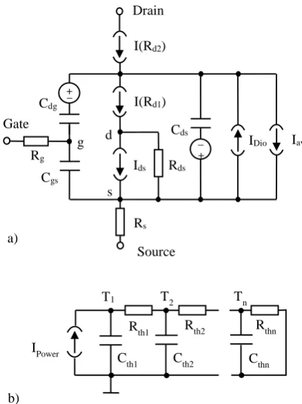
Fig. 2: Model of the SiC Power MOSFET, a) electrical subcircuit, b) thermal equivalent circuit.
current source I(Rd2). If the node voltages mentioned in the
following text are labeled with indices with capital letters they are referred to the external contacts of the device; whereas node voltages having indices with lowercase letters refer to internal nodes of the model.
The model has been implemented in the circuit simulator PSpice, but the modeling concept is in principle transferable to other simulation software.
A. DC-Current
SiC MOSFETs have a very large number of interface traps at the SiC-oxide interface. These traps degrade the device performance by reducing the electron density and electron mobility in the transistor channel [17]. Since the trap densities and their occupation with electrons are very temperature dependent they have also a significant influence on the temperature characteristic of the SiC MOSFET.
Taking the charge density of traps σit into account the
electron charge density σn in the channel is given (in the
case of constant electrostatic potential along the channel) by:
it th gs ox
n
c
V
V
(
)
(1)Vth is the threshold voltage of the transistor. The occupation
of the interface traps increases with increasing gate voltage until all traps are filled and σit saturates. This is described
with the equation:
itsat th gs ox it
th gs ox it
it
f
c
V
V
V
V
c
f
)
(
1
)
(
(2)fit is a parameter with a value less than 1. σitsat causes a shift
of the threshold voltage:
ox itsat th
c
V
(3)The electron charge density σn is then given by:
geff ox
th th gs it
it th
gs ox n
V
c
V
V
V
f
f
V
V
c
/
)
(
1
1
)
(
(4)
An effective gate voltage Vgeff is introduced to describe this
effect. Vgeff is limited to positive values (Vgs ≥ Vth); an
accurate description of the subthreshold behavior is not included in the model as it is of lesser importance. The leakage current of the MOSFET in its off-state is just taken into account with a temperature dependent resistor between drain and source.
For Vds > 0 the electron density decreases along the channel
(in y-direction) due to the increasing electrostatic potential. The dependence of σn on the channel potential is calculated
with a linear approximation and the influences of varying depletion charge and trap density are considered with a parameter k.
( )
)
(y coxVgeff kVch y
n
(5)Vch(y) is the difference of the electrostatic potential between
y and y = 0 (source side of channel). Gate
Iav
Source d
s g
Drain
Rg
Rs I(Rd2)
Ids
IDio Cdg
Cgs
Cds
Rds I(Rd1)
+ _
+ _
a)
IPower
Cth1 Cth2 Cthn
Rth1 Rth2 Rthn
T1 T2 Tn
b)
Source Source
oxide
Gate
n
-epi-layer
n
+ substratep-body
n
+Drain
p
+electrons
p
[image:2.595.59.278.319.612.2]With this description of the electron charge and taking into account the influence of the lateral electric field on the electron mobility the following expression is obtained for the transistor current in the linear region:
ds ds geff
sat ds
ds V V
k V g
V
I
2
1
(6)At high drain voltages the electrons near the end of the transistor channel reach their saturation velocity due to the high electric field. The electron current is then determined by the electron density near the channel end (given by eqn. (5)) and the saturation velocity vsat.
)
(
)
(
geff dsat sat geff dsatsat ox
dsat
wc
v
V
kV
g
V
kV
I
(7)
Vdsat is the drain-source voltage value where current
saturation begins. It is calculated by equating (6) and (7). The result is:
k
g
V
k
V
V
sat geff geff dsat
2
1
1
2
(8)This leads to the current equation in saturation:
geff sat geff
sat
geff dsat
V k g k V g k
V I
2 1 2
(9)
To combine the descriptions of the linear and of the saturation region of operation into a single expression an effective drain-source voltage Vdeff is used:
ds dsat ds dsat dsat
deff V V V V V
V 0.5
2 4
(10) Vdeff replaces Vds in eqn. (6). δ is a parameter which allowsto adjust the smoothness of the transition between the two operation regimes.
The parameter β depends on the electron mobility μn.
n ox
c
l
w
(11)The mobility in the transistor channel is strongly influenced by scattering due to the roughness of the SiC surface and by Coulomb scattering caused by the charge of the interface traps (besides the influence of the electric field which is already accounted for in the current equation).
The scattering due to surface roughness increases with increasing gate voltage due to the stronger attraction of the electrons to the SiC surface.
The Coulomb scattering due to the interface traps reduces the mobility mainly at low gate voltages. A large part of the
traps is already occupied below the threshold of the transistor. This is considered with the resulting value of Vth;
eqn. (2) describes just the increase of the trap occupation above the threshold voltage. Despite the further increase of the interface charge density above Vth the Coulomb
scattering becomes weaker because of a screening of the interface charge by the charge of the electrons in the inversion layer.
As a consequence of these different effects the β of a SiC MOSFET can increase with the gate voltage at low voltage levels above Vth and just at high values of Vgs a decrease is
observed like in Si MOSFETs. This behavior of β is described with the equation:
geff
geff V V
V
b
) / ' 1 ( 1
0 (12)
V’geff is equal to Vgeff if Vgeff is below Vβ and it is limited to
Vβ if Vgeff exceeds this value.
When the MOSFET is in saturation the drain current is not really constant; it increases further with rising drain voltage. This is caused mainly by channel length modulation and this effect is taken into account with a simple linear approximation and a parameter λ. The resulting current equation is then:
1 ( )
2 1
deff ds deff
deff geff
deff sat
ds V V V V
k V V g
I
(13) This result is also used for the case of reverse bias of the transistor (Vds< 0); in this case just a minus sign is added
to the right-hand side of (13), Vgs is replaced by Vgd in the
expression for Vgeff and the absolute value of Vds is used in
Vdeff.
If Vds is negative the body diode of the MOSFET structure
is also turned on. Due to the large bandgap of SiC a significant diode current flows only if Vds is below ca.
-2.5 V.
B. Drain Resistance
The higher critical electric field of SiC in comparison to silicon allows a much thinner blocking layer with higher doping concentration resulting in a much lower resistance. But the resistance of the drain region of SiC MOSFETs has still an important influence on the device characteristic. It causes a contribution to the on-state resistance which is not negligible. At low drain voltages the drain resistance is approximately constant and for this case it would be sufficient to include it in the model with just a resistor. However, at larger drain voltages the situation is different. The resistance of the drain region increases significantly as consequence of mainly two effects:
region directly below the gate oxide becomes depleted when the electrostatic potential in this region exceeds the gate voltage. This leads to a further strong constriction of the current path.
2. The high electric field at high drain voltage reduces the electron mobility.
The large drain resistance has the effect that at high drain voltages a large part of the voltage drops across the drain region and only a fraction of it remains across the transistor channel. This has mainly two consequences for the current characteristic:
1. When the voltage across the channel reaches the value Vdsat at which the saturation region of the MOSFET
begins, the voltage VDS which is externally applied at
the contacts of drain and source is much higher than Vdsat. This effect increases with increasing current i.e.
with increasing gate voltage. This means that the transition from linear to saturation region is shifted to significantly higher voltage levels of VDS.
2. When the MOSFET is in saturation the current increase caused by channel length modulation is strongly attenuated since the voltage across the channel increases only slightly with rising VDS.
This behavior of the SiC MOSFET at high voltage and current levels should also be reproduced by a compact model with sufficient accuracy. This is necessary to obtain correct simulation results of the switching waveforms and switching losses when the MOSFET is operated under hard switching conditions with inductive load. The model should also be able to predict the losses and the self-heating in the short-circuit case when very high drain voltages can occur.
The reduced effect of channel length modulation could be simply considered with an adjusted parameter in the equation of the electron current (eqn. (13)). But for an accurate modeling of the transition from linear to saturation region and to obtain correct results for the shift of the current saturation to high drain voltages it seems to be unavoidable to describe the voltage dependence of the drain resistance. However, it is rather difficult to consider the effects causing the variation of the resistance in a compact model.
For Si power MOSFETs already many attempts have been made to solve this problem [22]-[26]. But the resulting models are rather complicated, negatively impacting on computational efficiency and stability of the simulation, and they usually require the knowledge of details about the device structure and doping profiles. Only few models of the SiC power MOSFET consider the variable drain resistance so far. The model in [12] uses an empirical function to describe the variation of the drain resistance with drain and gate voltage and with temperature. The model presented in [13] depends on parameters which are related to the manufacturing process. In [14] a resistance model is developed which is based on the modeling approaches for silicon DMOS transistors. But this model is not incorporated into a compact model for circuit simulations. In [15] the drain resistance is modelled with a nonlinear voltage source and a resistance network; this model has only an implicit solution and the large number
of nodes of the resistive network has a negative impact on computation time.
This paper presents an approach which is based on substantial simplifications leading to a very simple solution which nevertheless provides results with reasonable accuracy.
The total resistance of the drain region is divided into two parts. The first part represents that region of the drain layer where the depletion regions cause a narrowing of the current path; the second part represents the rest of the drain where the full cross-section area remains available for the current.
1 1 1 1
A qN
l R
n
d
A qN
l L R
n d
2 1
2
(14)
l1 is the thickness of the region with an averaged reduced area A1; L is the total thickness of the drain region (low doped epi-layer), and A is its total area.
N is the doping concentration of the drain.
The decrease of the electron mobility at high electric fields is taken into account with the formula:
1 1 0
0 1
1 l v
V
sat R
n
(15)
VR1 is the voltage drop across the first part of the drain region. An equivalent expression is used for the mobility in the second part of the drain.
The following equation of Rd1 is then obtained:
1 1 1 0 1 1 1
0 1
A A I V L l R A
A A qNv
V L l A qN
L R
sat R d
sat R
d
(16) The result for Rd2 is correspondingly:
sat R d
d
I
V
L
l
R
R
1 20
2
1
(17)The thickness l1 depends on the expansion of the depletion region into the depth of the drain layer (in x-direction). Neglecting the (shallow) depth of the p-bodies l1/L can be approximately calculated by:
i R ds l
V V F L l
11
1
(18)
Φi is the built-in voltage of the pn-junctions. The parameter
dg r ds
r V a V
a A
A
2 1
1
1
(19)
The term with Vds and the parameter ar1 describes the area reduction due to the depletion regions of the pn-junctions, and the term with Vdg and the parameter ar2 considers the additional effect of the depletion region under the gate oxide which is formed when the electrostatic potential in this region exceeds the gate voltage. Only the positive voltage range of Vds and Vdg is used in (18) and (19); the
variables Vds and Vdg are set to zero if the voltages have
negative values.
Since Φi is a parameter used for the voltage-dependent
drain-source capacitance and Fl is determined by the
breakdown voltage, four parameters are used for the modeling of the drain resistance.
The value of Rd0 is important for the on-state voltage of the MOSFET, ar1 has a strong influence on the transition from linear to saturation region, ar2 influences slightly the saturation characteristic at high drain voltages, Isatgives an
upper limit of the current which can flow through the drain layer.
With an additional constant factor in Rd2further resistance
components resulting from substrate layer, contact and package can also be included.
C. Further Model Components
The voltage-dependent capacitances of the SiC-MOSFET are modeled with a capacitor of fixed value in series with a controlled voltage source (Fig. 2). The voltage source provides such a voltage across the capacitor that the product of voltage and capacitance results in the required value of the charge [27].
The temperature dependence of the SiC-MOSFET is considered by describing the variation of the model parameters with temperature. Self-heating can also be simulated with the help of a thermal network which consists of a current source and one or several pairs of thermal capacitances and thermal resistances (Fig. 2b). The current IPower of the current source corresponds with the
total power dissipated in the device which is calculated as the sum of the current and voltage products of all current sources and resistors of the MOSFET model. The voltages at the thermal capacitances are equivalent to a temperature rise which is added to the ambient temperature.
A further effect included in the model is the breakdown behavior (Iav in Fig. 2).
III. RESULTS
A. Comparison of Model and Device Simulations
Simulations with the device simulator SENTAURUS [19] have been used to support the model development and to validate the model results. The analyzed structure is shown in Fig. 1. The dimensions and doping concentrations have been chosen in such a way that the characteristics of a 1.2 kV SiC MOSFET, manufactured by Cree Inc. (CMF2010D [28]), could be reproduced. The density of interface traps at
the semiconductor-oxide boundary has been selected according to the analysis presented in the paper [17] and to adjust the IDS(VGS)-curve to the experimental result.
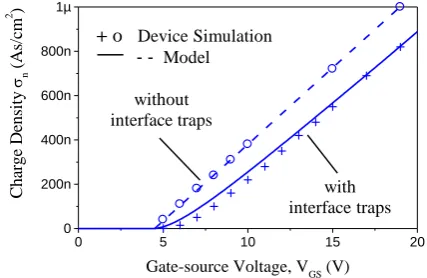
The influence of the interface traps on the electron charge in the transistor channel can be seen in Fig. 3. It shows how the electron charge density σn increases with the gate
voltage in the cases with and without interface traps. Without traps a linear increase of the electron density with rising VGS results (except for a very small voltage range at
[image:5.595.317.531.245.384.2]threshold). Interface traps reduce the electron density and a linear dependence on the gate voltage is obtained only for larger values of VGS when all traps are occupied.
Fig. 3 also shows how this behavior is described with the model equation for σn (4).
Fig. 3: Electron charge density in transistor channel.
[image:5.595.317.523.512.652.2]The effect of the drain resistance on the internal source voltage is demonstrated in Fig. 4. The internal drain-source voltage is obtained by subtracting the voltage drop occurring along the current path in the drain region from the voltage which is externally applied at the drain and source contacts. This internal voltage corresponds with the voltage Vdswhich is used in the model equations.
Fig. 4: Internal drain-source voltage Vds = VDS - VRd.
With rising drain voltage the drain resistance increases significantly due to the constricted current path and causes a large voltage drop in the drain. This retards the increase of the voltage across the transistor channel especially at high gate voltage which has the consequence that the current saturation of the transistor is reached only at rather high values of the drain voltage.
0 5 10 15 20
0 200n 400n 600n 800n 1µ
C
h
ar
g
e
D
en
si
ty
n
(
A
s/
cm
2 )
Gate-source Voltage, VGS (V)
0 10 20 30 40 50
0 5 10 15 20
VDS
V
Rd
(
V
)
Drain-source Voltage, VDS (V) with interfacetraps without
interface traps + o DeviceSimulation
- - Model
VGS = 15 V
VGS = 20 V
+ Device Simulation
Measurement
Model When the drain region below the gate oxide begins to be
depleted the electrostatic potential remains nearly constant at a point close to the pn-junctions where the electrons are injected from the transistor channel into the drain. Therefore the internal drain-source voltage becomes limited to a value which is approximately equal to the gate-source voltage.
The comparisons of the results produced by the model and extracted from device simulations show that the simple model of the drain resistance can describe the basic effects with the sufficient accuracy necessary to obtain the current-voltage characteristics correctly.
B. Comparison with Measurements
The model has been compared with measurements of a few different SiC Power MOSFETs which are available from device manufacturers so far. As example the results obtained with the newest SiC-MOSFET from Cree Inc. are presented. It is a 1.2 kV, 30 A transistor (C2M0080120D [28]).
Fig. 5 shows the transfer characteristics of the measured device and the model at different temperatures.
Fig. 5: Transfer characteristics at different temperatures, VDS = 10 V.
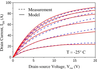
Fig. 6 to Fig. 8 demonstrate the output characteristics at room temperature, -25°C, and 200°C, respectively.
Fig. 6: Output characteristics at room temperature. The gate-source voltage varies from 10 V to 20 V with increments of 2 V.
Fig. 7: Output characteristics at -25° C. The gate-source voltage varies from 10 V to 20 V with increments of 2 V.
Fig. 8: Output characteristics at 200° C. The gate-source voltage varies from 10 V to 20 V with increments of 2 V.
At high temperatures the large resistance of the drain region causes a significant limitation of the current. At low temperature the reduced electron mobility in the transistor channel is the main reason for the current limits.
The variation of the drain-source on-state resistance Ron
with temperature is shown in Fig. 9.
Fig. 9: Variation of the on-state resistance with temperature.
0 2 4 6 8 10 12 14 16 18 20 0
10 20 30 40
D
ra
in
C
u
rr
en
t,
IDS
(
A
)
Gate-source Voltage, VGS (V)
0 5 10 15 20
0 20 40 60 80 100
D
ra
in
C
u
rr
en
t,
IDS
(
A
)
Drain-source Voltage, VDS (V)
0 5 10 15 20
0 20 40 60 80 100
D
ra
in
C
u
rr
en
t,
IDS
(
A
)
Drain-source Voltage, VDS (V)
0 5 10 15 20
0 20 40 60
D
ra
in
C
u
rr
en
t,
IDS
(
A
)
Drain-source Voltage, VDS (V)
-50 0 50 100 150 200
0.05 0.10 0.15 0.20 0.25
Ron
(
)
Temperature (°C) Measurement
Model T = 200° C
T = 20° C
T = -25° C
T = 20° C Measurement
Model
Measurement
Model
+ Measurement
Model
T = -25° C
T = 200° C
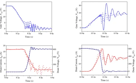
[image:6.595.319.518.82.222.2] [image:6.595.318.517.283.424.2] [image:6.595.66.263.348.485.2] [image:6.595.320.528.562.700.2] [image:6.595.64.267.569.704.2]Fig. 10: Turn-off and turn-on behavior of the SiC-MOSFET with inductive load and freewheeling diode at T = 150°C, - - - measurement, simulation.
The switching behavior has been investigated with a test circuit consisting of the SiC-MOSFET, an inductive load of 320 µH and a SIC Schottky diode used as freewheeling diode. In the simulated circuit the parasitic inductances of the device packages and the connections between the circuit components as well as the parasitic capacitance of the inductive load are considered. The gate drive is simplified with just a pulsed voltage source and a gate resistor. For the Schottky diode a model provided by CREE is used.
Fig. 10 shows the waveforms of gate-source voltage, drain-source voltage and drain current which are obtained by measurements and by simulations at turn-off and turn-on of the SiC-MOSFET.
The agreement between simulation and measurements is quite good for the main switching characteristics like the voltage and current slopes. Major differences are just observed for some oscillations. For the turn-off transient the current ringings are much larger in the experiment than in the simulation; for the turn-on transient the ringings of the gate voltage are larger in the simulation than in the measurement. But it is actually rather difficult to reproduce all oscillations correctly since the parasitic elements of the circuit are considered just in a very simplified way and also the influence of the measurement tools is neglected.
IV. CONCLUSION
A compact model of SiC Power MOSFETs has been developed which reproduces the device behavior with good
accuracy for the whole range of operating biases and temperatures. This has been achieved by taking into account the physical phenomena which are responsible for the special characteristics of SiC MOSFETs. Interface traps at the SiC-oxide interface reduce the electron density and electron mobility in the transistor channel, and they cause a variation of the mobility with gate voltage and temperature which is (at low Vgs) contrary to that in Silicon
MOSFETs. The resistance of the drain region increases strongly with the drain voltage and the resulting voltage drop at high current levels is decisive for the current-voltage characteristics.
To keep the calculation as simple as possible and to obtain a better fit empirical functions and parameters are partly used, but they are closely related to the physical phenomena which are the origin of the device behavior.
Due to the inclusion of the relevant effects and the accuracy over a very broad voltage and temperature range the model is well suited to investigate the behavior of SiC MOSFETs with the help of circuit simulations in many diverse applications. The advantages of SiC MOSFETs as well as possible problems can be explored and the capability to simulate fast transient self-heating effects can also support the analysis of performance and robustness.
REFERENCES
[1] H.A. Mantooth, K. Peng, E. Santi, J.L. Hudgins, “Modeling of Wide Bandgap Semiconductor Devices – Part I,” IEEE Trans. Electron Devices, vol. 62, no. 2, pp. 423-433, Feb. 2015.
9.0µ 9.1µ 9.2µ 9.3µ 9.4µ -5
0 5 10 15 20
D
ra
in
C
u
rr
en
t,
IDS
(
A
)
Time (s)
0 200 400 600
D
ra
in
V
o
lt
ag
e,
V
DS
(
V
)
12.0µ 12.1µ 12.2µ 12.3µ 12.4µ 0
10 20 30
D
ra
in
C
u
rr
en
t,
IDS
(
A
)
Time (s)
0 200 400 600
D
ra
in
V
o
lt
ag
e,
V
DS
(
V
)
9.0µ 9.1µ 9.2µ 9.3µ 9.4µ 0
5 10 15 20
G
at
e
V
o
lt
ag
e,
V
GS
(
V
)
Time (s)
12.0µ 12.1µ 12.2µ 12.3µ 12.4µ 0
10 20 30
G
at
e
V
o
lt
ag
e,
V
GS
(
V
)
[2] T. McNutt, A. Hefner, A. Mantooth, D. Berning, S.H. Ryu, “Silicon Carbide MOSFET Model and Parameter Extraction Sequence,” IEEE Trans. Power Electron., vol. 22, no. 2, pp. 353-363, March 2007.
[3] J. Wang, T. Zhao, A.Q. Huang, R. Callanan, F. Husna, A. Agarwal, “Characterization, Modeling and Application of 10-kV SiC MOSFET,” IEEE Trans. Electron Devices, vol. 55, no. 8, pp. 1798-1806, August 2008.
[4] N. Phankong, T. Funaki, T. Hikihara, “A Static and Dynamic Model for a Silicon Carbide Power MOSFET,” in 13th European Conf. Power Electronics and Applications, 2009, pp. 1-10.
[5] R. Pratap, R.K. Singh, V. Agarwal, “SPICE Model Development for SiC Power MOSFET,” in IEEE Int. Conf. Power Electronics, Drives and Energy Systems, 2012, pp. 1-5.
[6] K. Sun, H. Wu, J. Lu, Y. Xing, L. Huang, “Improved Modeling of Medium Voltage SiC MOSFET,” IEEE Trans. Power Electron., vol. 29, no. 5, pp. 2229-2239, May 2014.
[7] M. Mudholkar, S. Ahmed, M.N. Ericson, S. Frank, C. Britton, A. Mantooth, “Datasheet Driven Silicon Carbide Power MOSFET Model,” IEEE Trans. Power Electron., vol. 29, no. 5, pp. 2220-2227, May 2014. [8] Y. Cui, M. Chinthavali, L.M. Tolbert, “Temperature
Dependent PSpice Model of Silicon Carbide Power MOSFET,” in Proc. 27th IEEE Appl. Power Electron. Conf. (APEC), Feb. 2012, pp. 1698-1704.
[9] S. Yin, T. Wang, K.J. Tseng, J. Zhao, X. Hu, “Electro-thermal Modeling of SiC Power Devices for Circuit Simulation,“ in Proc. 39th IEEE Conf. Ind. Electron. Soc. (IECON), Nov. 2013, pp. 718-723.
[10] P. Alexacis, O. Alatise, L. Ran, P. Mawby, “Modeling Power Converters Using Hard Switched Silicon Carbide MOSFETs and Schottky Barrier Diodes,” in Proc. 15th Eur. Conf. Power Electron. Appl. (EPE), Sep. 2013, pp. 1-9.
[11] A. Merkert, T. Krone, A. Mertens, “Characterization and Scalable Modeling of Power Semiconductors for Optimized Design of Traction Inverters with Si- and SiC-Devices,” IEEE Trans. Power Electron., vol. 29, no. 5, pp. 2238-2245, Jan. 2014.
[12] V. d’Alessandro, A. Magnani, M. Riccio, G. Breglio, A. Irace, N. Rinaldi, A. Castelazzi, “SPICE Modeling and Dynamic Electrothermal Simulation of SiC Power MOSFETs,” in Proc. IEEE 26th Int. Symp. Power Semiconductor Devices and IC’s (ISPSD), June 2014, pp. 285-288.
[13] G.D. Licciardo, S. Bellone, L. di Benedetto, “Analytical Model of the Forward Operation of 4H-SiC Vertical DMOSFET in the Safe Operating Temperature Range,”
IEEE Trans. Power Electron., vol. 30, no. 10, pp. 5800-5809, Oct. 2015.
[14] M. Hasanuzzaman, S.K. Islam, L.M. Tolbert, B. Ozpinezi, “Design, Modeling, Testing and SPICE Parameter Extraction of DIMOS Transistor in 4H-Silicon Carbide,” Int. J. High-Speed Electron. Syst., vol. 16, no. 2, pp. 733-746, 2006.
[15] R. Fu, A. Grekov, J. Hudgins, A. Mantooth, E. Santi, “Power SiC DMOSFET Model Accounting for Nonuniform Current Distribution in JFET Region,”
IEEE Trans. Industry Appl., vol. 48, no. 1, pp. 181-190, Jan/Feb 2012.
[16] S.K. Powell, N. Goldsman, J.M. McGarrity, J. Bernstein, C.J. Scozzie, A. Lelis, “Physics-based Numerical Modeling and Characterization of
6H-Silicon-Carbide Metal-Oxide-Semiconductor Field-Effect Transistors,” J. Appl. Phys., vol. 92, no. 7, pp. 4053-4061, Oct. 2007.
[17] S. Pothbare, N. Goldsman, A. Lelis, McGarrity, M. James, McLean, F. Barry, D. Habersat, “A Physical Model of High Temperature 4H-SiC MOSFETs,” IEEE Trans. Electron Devices, vol. 55, no. 8, pp. 2029-2040, August 2008.
[18] B.N. Pushpakaran, S.B. Bayne, A.A. Ogunniyi, “Electro Thermal Transient Simulation of Silicon Carbide Power MOSFET,” in Proc. 19th IEEE Pulsed Power Conf. (PPC), June 2013, p.1.
[19] Sentaurus Device Simulator
http://www.synopsys.com/Tools/TCAD/DeviceSimula tions
[20] F.N Masana, “A Straightforward Analytical Method for Extraction of Semiconductor Device Transient thermal Parameters,” Microelectronics Reliability, vol. 47, issue 12 Dec. 2007, pp. 2122-2128.
[21] A. Castellazzi, “Comprehensive Compact Models for the Circuit Simulation of Multichip Power Moduls,”
IEEE Trans. Power Electron., vol. 25, no. 5, pp.1251-1264, May 2010.
[22] C. Kreutzer, N. Krischke, P. Nance, “Physically Based Description of Quasi-Saturation Region of Vertical DMOS Power Transistors,” in Int. Electron Device Meeting, 1996 , pp. 489-492.
[23] J. Victory, C. McAndrew, R. Thoma, “A 3D Physically Based Compact Model for IC VDMOS Transistors,” in
Proc. 21st Int. Conf. Microelectronics, pp. 399-402, 1997.
[24] C. Tsai, D.E. Burk, K.D.T. Ngo, “Physically Modeling of the Power VDMOST for Computer-Aided Design of Integrated Circuit,” IEEE Trans. Electron Devices, vol. 44, no. 3, pp. 472-480, March 1997.
[25] W. Manhawy, W. Fikry, “Power MOSFET Macromodel Accounting for Saturation and Quasi-Saturation Effect,” in Canadian Conf. Electrical and Computer Engineering, 2004, pp. 1839-1843.
[26] A. Bazigos, F. Krummenacher, J.M. Sallese, M. Bucher, E. Seebacher, W. Posch, K. Molnar, M. Tang, “A Physics-Based Analytical Compact Model for the Drift Region of HV-MOSFET,” IEEE Trans. Electron Devices, vol. 58, no. 6, pp. 1710-1721, June 2011. [27] A. Castellazzi, Y. Gerstenmeier, R. Kraus, G.K.M.
Wachutka, “Reliability Analysis and Modeling of Power MOSFETs in the 42-V-Power Net,” IEEE Trans. Power Electron., vol. 21, no 3, pp. 603-612, May 2006. [28] Datasheets of SiC Power MOSFETs CMF20120D and
C2M0080120D http://www.cree.com/products
Dr. Rainer Kraus
Department of Electrical Engineering and Information Technology
University of Bundeswehr
Werner- Heisenberg-Weg 39, 85577 Neubiberg, Germany E-Mail: [email protected]
Prof. Dr. Alberto Castellazzi
Power Electronics, Machines and Control Group University of Nottingham
NG7 2RD Nottingham, UK