VERSION 0 .00
S M
Y S i c
0 T E
r 0
SYSTEM REF ERENCE MANUAL I M
MEN S I
o
N 6 8 0 0 0R E F E R E N C E MAN U A L C r a f t C 0 r p 0 r a t i o n
YERSIOII 0.00
NOT ICE
Micro Craft Corporation reserves the right to make improvements in the product described in this manual at any time and without notice.
DISCLAIMER OF ALL WARANTIES AND LIABILITY
-MICRO CRAFT CORPORATION MAKES NO WARRANTIES, EITHER EXPRESS OR IMPLIED, WITH RESPECT TO THIS MANUAL OR WITH RESPECT TO THE SOFTWARE DESCRIBED IN THIS MANUAL, ITS QUALITY, PERFORMANCE, MERCHANTIBILITY, OR FITNESS FOR ANY PARTICULAR PURPOSE. MICRO CRAFT CORPORATION SOFTWARE IS SOLD OR LICENSED "AS IS." THE ENTIRE RISK AS TO ITS QUALITY AND PERFORMANCE IS WITH THE BUYER. SHOULD THE PROGRAMS PROVE DEFECTIVE FOLLOWING THEIR PURCHASE, THE BUYER (AND NOT MICRO CRAFT COPPORATION, ITS DISTRIBUTOR, OR ITS RETAILER) ASSUMES THE ENTIRE COST OF ALL NECESSARY SERVICING, REPAIR, OR CORRECTION AND ANY INCIDENTAL OR CONSEQUENTIAL DAMAGES. IN NO EVENT WILL MICRO CRAFT CORPORATION BE LIABLE FOR DIRECT, INDIRECT, INCIDENTAL, OR CONSEQUENTIAL DAMAGES RESULTING FROM ANY DEFECT IN THE SOFTWARE, EVEN IF MICRO CRAFT CORPORATION HAS BEEN ADVISED OF THE POS-SIBILITY OF SUCH DAMAGES. SOME STATES DO NOT ALLOW THE EXCLUSION OR LIMITATION OF IMPLIED WARRANTIES OR LIABILITY FOR INCIDENTAL OR CONSE-QUENTIAL DAMAGES, SO THE ABOVE LIMITATION OR EXCLUSION MAY NOT APPLY TO
YOU.
This manual is copyrighted. All rights are reserved. This document may not, in whole or in part, be copied, photocopied, translated, or reduc-ed to any electronic medium or machine readable form without prior consent, in writing, from Micro Craft Corporation.
Copyright 1983 by Micro Craft Corporation Micro Craft Corporation
4747 Irving Blvd. Dallas, Texas 75247
(214) 630-2562
VERSION 0.00
Additional copies of this manual may be ordered from your DEALER
by using the MICRO CRAFT part number 680-0001-200.
Ask your DEALER also for a
free brochure with a complete list of a Micro Craft manuals and products
MICRO CRAFT CORPORATION Customer Support Department
4747 Irving Blvd. Dallas, Texas 75247
Page i
Page ii
Pg. 1 Pg. 3 Pg. 5 Pg. 9 Pg. 9 Pg. 9 Pg. 9 Pg. 10 Pg. 10 Pg. 10 Pg. 10 Pg. 10 Pg. 11 Pg. 13 Pg. 15 Pg. 15 Pg. 15 Pg. 16 Pg. 16 Pg. 16 Pg. 17 Pg. 18 Pg. 19 Pg. 20 Pg. 21 Pg. 21 Pg. 22 Pg. 22 Pg. 22 Pg. 22 Pg. 23 Pg. 23 Pg. 23 Pg. 24 Pg. 24 Pg. 25 Pg. 25 Pg. 26 Pg. 26 Pg. 27 Pg. 27 Pg. 28 Pg. 29 Pg. 29 Pg. 31 Pg. 33 Pg. 33 Pg. 35
INTRODUCTION WELCOME
TABLE OF CONTENTS
CHAPTER 1 - OVERVIEW POWER SUPPL Y MAIN BOARD KEYBOARD
KEYBOARD
KEYBOARD INTERFACE CRT
PROCESSOR MEMORY I/O
EXPANSION SLOTS CHAPTER 2 - HARDWARE
POWER SUPPL Y MAIN BOARD
Jl - POWER
J2 - RESET SWITCH ASSEMBLY J3 - KEYBOARD
J4 - VIDEO OUTPUT
VERSION 0.00
J5 - MINI STANDARD DISKETTE CONNECTOR (34 pin) J6 - PARALLEL PRINTER PORT
J7 - STANDARD DISKETTE CONNECTOR (50 pin) J8 - RS-232C INTERFACE
J9 - GAME CONTROL (A/D) J10 SPEAKER
Jll - LIGHT PEN
J12 - NOT USED AND NOT PHYSICALLY PRESENT J13 - AUTO LINE FEED
J14 - AUXILIARY VIDEO KEYBOARD
KEYBOARD
KEYBOARD INTERFACE PRINTER OUTPUT
RS-232
REAL TIME CLOCK CRT
SPEAKER DISK DRIVES MC68000 INTERRUPTS MEMORY
EXPANSION SLOTS CO-PROCESSORS
CHAPTER 3 - MEMORY ALLOCATION MEMORY CIRCUITRY
MEMORY MAP USES
VERSION 0.00 Page iii
Pg. 37 Pg. 39 Pg. 39 Pg. 40 Pg. 41 Pg. 42
Pg. 43
Pg. 43
Pg. 43
Pg. 44
Pg. 44 Pg. 45 APPENDICES Pg. A-l Pg. B-1 Pg. C-1 Pg. 0-1 Pg. E-l Pg. F-1
CHAPTER 4 - CP/M-68K, CPMBIOS, and ROMBIOS FLOW
ADDITIONAL CALLS
FUNCTION 256 - Change DIskette Drive Format FUNCTION 257 - Read Diskette Drive Format
FUNCTION 258 - Set the Physical Parameter Table, Set the CP/M Disk Parameter Table, or Set the Disk Interlace Table
TERMINAL ATTRIBUTES CONTROL FUNCTIONS ESCAPE SEQUENCES ROMBIOS
ROMBIOS FUNCTIONS INPUT/OUTPUT
TOOL-KIT KEYBOARD CODES ASCII CODES
EXPANSION SLOT PINOUTS DIRECT I/O
ROMBIOS
Page iv VERSION 0.00
YERSION 0.00 Page 1
I N T ROD U C T ION
VERSIOII 0.00 Page 3
WELCOME TO THE DIMENSION 68000
You are now the owner of the most powerful most compatible, most flex-ible micro computer available in the world today. You, also, may be as-sured that the designers of Dimension 68000 intend that the statement above will be true for many years to come!
This manual is a tool for gaining an in-depth understanding of the op-eration of the DIMENSION 68000. It is NOT a tutorial. It is a collec-tion of facts and other data.
Page 4 VERSION 0.00
tERSIOIII 0.00 Page 5
C HAP T E R 1
o
V E R V lEWYERSIOII 0.00 Page 7
The DIMENSION 68000 system is made up of several functional components or systems. Those syst,ems are:
- The power Supply - The Main Board - The Keyboard - The CRT Interface - The Processor (CPU) - The Memory
- The I/O (Input/Output) - The Expansion Slots
- The Floppy Disks and Controllers
These systems, together, handle all of the operations that are perform-ed by the DIMENSION 68000.
This manual often gives directional instructions for the location, by the user, of various systems, parts, and components. In this manual, all directional instructions will refer to the orientation depicted in the view (looking down on the top) below:
Page 8 VERSION 0.00
The directions "Front" and "down" are towards the diskette drives and the reset switch. The directions "back" and "up" are away from the drives and toward the REAR PANEL.
To remove the top cover from the system unit of the DIMENSION 68000, use the following steps:
- TURN OFF the POWER
- TURN the system unit over (upside down)
- USING a PHILLIPS HEAD SCREWDRIVER, LOOSEN the SIX (6) SCREWS that are holding the top cover. These screws are NOT removable from the bottom cover of the system unit. The screws are designed to be held captive in the bottom cover so that they will not be lost.
- with the loosened cover still in place, TURN the system unit back over (right side up)
- LIFT off the top cover
Looking down upon the system unit (with the top cover removed), the system unit looks like the picture below.
VERSION 0.00 Page 9
The POWER SUPPL Y
The POWER SUPPLY is enclosed in the metal cover on the right side in-side the system unit. It supplies +5 VDC @ 8 A., +12 VDC @ 2.5 A., and -12 VDC @ 2 A. It is a high-frequency "switching"-type power supply.
The MAIN BOARD
The MAIN BOARD is the large printed circuit board which takes u~ most of the bottom of the case of the system unit. The MAIN BOARD IS the actually the computer.
On the MAIN BOARD are the integrated circuits, components, and the ex-pansion slots. The microprocessor (or "brain") of the DIMENSION 68000 is the Motorola (or equivalent) MC68009L8 device. The 68900 has an ad-dressing capacity of 16 M Bytes. The MAIN BOARD can have up to 512 K Bytes of RAM (Random Access Memory) in 128 K Byte increments.
Also, on the MAIN BOARD are 8 K Bytes of ROM (Read Only Memory). The ROM is used to hold the system MONITOR and the ROMBIOS.
The six long peripheral slots that are toward the middle back of the MAIN BOARD can each hold a card. The cards can be anyone of the fol-lowing types:
- An Emulator Card (examples; Z-80, 8086, and 6512) - A Memory Expansion Card
- A Hard Disk Controller - A Peripheral Controller - A Peripheral Device
The KEYBOARD System
The Keyboard system is composed of two parts; the Keyboard and the Key-board Interface.
The Keyboard
The Keyboard unit, that plugs into the back of the DIMENSION 68000 sys-tem unit, is a microprocessor controlled assembly that is capable of handling in excess of 30 characters per second. The Keyboard assembly transmits the characters, that are typed in, to the DIMENSION 68000 system using the following characteristics:
- 30 characters/second - 8 bit characters
- ASCII (American Standard Code for Information Interchange) encoding - asynchronous transmission
Page 10 VERSION 0.00
The Keyboard Interface
The Keyboard Interface circuitry receives the characters from the Key-board assembly. The asynchronous transmission technique adds a "start" bit and adds a "stop" bit to each character, and then transmits the character, with the added bits, in a serial mode, from the Keyboard as-sembly to the Keyboard Interface. The Keyboard Interface removes the added "start" and "stop" bits from each character received, and con-verts the character from a serial mode to a parallel mode. This is im-plemented using one serial channel of the Signetics 2681 Dual Universal Asynchronous Receiver/Transmitter (DUART) chip.
The CRT Interface
The CRT Interface provides a video output signal for the connection of a CRT or other video display device. The CRT interface supplies a video signal with the following characteristics:
- RS-170 compatible signal - Composite video (sync + video)
- Capable of COLOR and MONOCHROME operation
The Processor (CPU)
The Processor (or CPU - Central processing Unit) is a Motorola MC68000 (or equivalent) microprocessor integrated circuit (or chip). The Moto-rola MC68000 device is internally a 32 Bit microprocessor. The MC68000 has 16 Bit wide data paths.
The Memory
There are two (2) types of memory in the DIMENSION 68000; RAM (Random Access Memory) and ROM (Read Only Memory). The Main Board can hold 128 K Bytes, 256 K Bytes, 384 K Bytes, or 512 K Bytes of RAM. The amount of RAM can be expanded from 512 K Bytes up to 16 M Bytes by using memory expansion cards. There are 8 K Bytes of ROM.
The I/O (Input/Output)
The I/O (Input/Output) for the DIMENSION 68000 system unit consists of the following devices:
- The Keyboard Interface - The CRT Interface - The Diskette Drives - The Parallel Printer Port - The RS-232C Interface - The Game Control Interface
YERSION 0.00 Page 11
Optionally, there can be connectors on the rear panel to c6nnect the following:
- Additional Mini (5 1/4", 3 1/2", 3 1/4", etc.) Diskette Drives - Additional 8 Inch (Full Size) Diskette Drives (up to four total)
The Expansion Slots
There are six (6) Expansion Slots inside the system unit. The Expansion Slots provide the capability to plug in various types of cards. Some of the types of cards are:
- Emulator Card(s)
- Hard Disk Interface Card
- RS-232 Ports Card(s) - 8 ports per card - Analog/Digital Interface Card(s)
- 512 K Byte RAM Memory Cards
It is expected that, in the future, Micro Craft Corporation and other manufacturers will be providing many types of cards to plug into the Expansion Slots.
Page 12 VERSION 0.00
ERStON 0.00 Page 13
C HAP T E R 2
HARDWARE
VERSION 0.00 Page 15
The POWER SUPPLY
The POWER SUPPLY for the DIMENSION 68000 is a high-frequency "switch-ing"-type unit. It supplies the following voltages and currents:
+5 VDC +,- 1% @ 8 Amps +12 VDC +,- 5% @ 2.S Amps -12 VDC +,- 5% @ 2 Amps
These voltages are supplied to the MAIN BOARD and to the Disk Drives. Power supplied to the MAIN BOARD is available to the Expansion Slots, and to the Game Control connector (J9) on the MAIN BOARD.
The POWER SUPPLY requires lIS VAC @ 3 Amps (MAX.) to operate. The POWER SUPPLY for the DIMENSION 68000, optionally, may be configured to oper-ate from 220 VAC power. The POWER SUPPLY input power, whether 115 VAC or 220 VAC, must be of a frequency in the range of from 50 Hz. to 400 Hz. The input power to the POWER SUPPLY is filtered for RFI (Radio Fre-quency Interference). The input power to the POWER SUPPLY also has po-wer line surge suppression applied.
The MAIN BOARD
The MAIN BOARD has the Expansion Slots, the integrated circuits (in-cluding the 68000 microprocessor), the components, and the connectors that link the MAIN BOARD to the POWER SUPPLY, the Keyboard, etc. The connectors on the MAIN BOARD are detailed below.
Jl
-
POWER4 S 6 PIN
I
\
1o 0 0 2
3
•
o 0 0 4 S+---+ 6
1 2 3 Top View of Connector on MAIN BOARD
SYSTEM REFERENCE MANUAL
USAGE
+S VDC GROUND +12 VDC +S VDC GROUND -12 VDC
The Connector Necessary to Mate with the Connector on the MAIN BOARD is made using a MOLEX PiN 03-09-1064
recepticle and MOLEX
PiN 02-09-1118 pins (or the equivalent).
Page 16
J2 - RESET SWITCH ASSEMBLY ++_._+
0 1 0 2 0 3
0 4 ++---+ Top view of Connector on MAIN BOARD
J3 - KEYBOARD
1 - \
I
\
I
\2
I
0 oI
\ 0 o
I
5 \ 0
I
4\
-3-I
View of Front 1 of PIN 1 2 3 4 USAGE RESET GROUND NORMAL LED POWER
The PAINT DOT indicates pin 1.
PIN USAGE 1 SIGNAL FROM
KEYBOARD 2
3
4 GROUND 5 +5 VDC POWER
TO KEYBOARD Connector at rear of
SYSTEM UNIT
J4 - VIDEO OUTPUT
CHAPTER 2
PIN USAGE Center SIGNAL Outside GROUND
VERSION 0.00
The Connector Necessary to Mate with the Connector on the MAIN BOARD is a MOLEX
PiN 22-26-9041 (or the equivalent) •
The Connector Necessary to Mate with the Connector at rear of SYSTEM UNIT is a 5 PIN, "DIN"-type, MALE
The Connector Necessary to Mate with the Connector on the REAR PANEL is an RCA type MALE
YERSION 0.00 Page 17
J5 - MINI STANDARD DISKETTE CONNECTOR (34 pin) +---+
+---+ o 0
o 0
o 0
o 0
o 0 o 0 o 0 ++
I
o 0
o 0
o 0
o 0 ++ o 0
o 0
o 0
o 0
o 0
o 0
I
1+---+ +---+ view of the Connector on the MAIN BOARD The PAINT DOT indicates pin 1
PIN 1 2 3 4 5 6 7 8 9 113 11 12 13 14 15 16 17 18 19 213 21 22 23 24 25 26 27 28 29 313 31 32 33 34
SYSTEM REFERENCE MANUAL
USAGE GROUND GROUND GROUND DRSEL 3 * GROUND INDEX* GROUND DRSEL 13 * GROUND DRSEL 1 * GROUND DRSEL 2 * GROUND GROUND M DIR * GROUND M STEP * GROUND M W DATA * GROUND WR ENA * GROUND GROUND GROUND RD DATA GROUND M HEAD * GROUND
The Connector Necessary to Mate with the Connector on the MAIN BOARD is an ANSLEY PiN 6139-34131313 (or
the equivalent)
NOTE: An * after a signal name indicates that the logic for that signal is inverted, that is to say that the signal is active on a "13" instead of a
"1".
Page 18 VERSION 0.00
J6 - PARALLEL PRINTER PORT
11\>]-
PIN USAGE The Connector Necessaryto Mate With the Connector 1 STROBE* on the REAR PANEL is an
[ ] 2 D0* Amphenol 36 Pin "Blue Ribbon"
[ ] 3 Dl* type
[ ] 4 D2*
[ ] 5 D3*
[ ] 6 D4* NOTE: An * after the signal
[ ] 7 D5* name indicates that
[ ] 8 D6* the logic for that
[ ] 9 D7* signal is inverted,
[ ] 10 ACKNLG* that is to say that
[ ] 11 RDY* the signal is active
[ ] 12 Not Connected on a "0" instead of
[ ] 13 Not Connected a "1".
[ ] 14 AUTO LINE FEED *
[ ] 15 Not Connected
[ ] 16 Not Connected
[ ] 17 GROUND
[ ] 18 Not Connected
19 GROUND
//==--
20 GROUND21 GROUND
22 GROUND
23 GROUND
24 GROUND
25 GROUND
26 GROUND
27 GROUND
28 GROUND
29 GROUND
30 GROUND
31 INIT*
32 Not Connected
33 GROUND
34 Not Connected 35 Not Connected 36 Not Connected
YERSIOM 0.00
J7 - STANDARD DLSKETTE CONNECTOR (50 pin) +---+
+---+ o
0
o 0
o 0 o 0
o 0
o 0
o 0 o 0
o 0 o 0
o 0 ++
001
o 0
o 0
o 0 ++ o 0
o 0
o 0
o 0
o 0
o 0
o 0
o 0
o 0
o 0
.1
+---+ +---+ View of the Connector on the MAIN BOARD The PAINT DOT indicates pin 1
PIN 1 2 3 4 5 6 7 8 9 10 11 12 13 14 15 16 17 18 19 20 21 22 23 24 25 26 27 28 29 30 31 32 33 34 35 36 37 38 39 40 41 42 43 44 45 46 47 48 49 50
SYSTEM REFERENCE MANUAL
USAGE GROUND M LOW C
*
GROUNDMOTOR OFF 0
*
GROUNDMOTOR OFF 1
*
GROUNDMOTOR OFF 2
*
GROUND2 SIDED
*
GROUND GROUND M HEAD*
GROUND GROUND M HEAD LD*
GROUND INDEX*
GROUND GROUNDMOTOR OFF 3
*
GROUNDDR SEL 0
*
GROUND DR SEL 1*
GROUND DR SEL 2*
GROUND DR SEL 3*
GROUND M DIR*
GROUND M STEP*
GROUND M W DATA*
GROUND WR ENA*
GROUND TK 00*
GROUND W PROT*
GROUND RD DATA GROUND GROUNDPage 19
The Connector Necessary to Mate with the Connector on the MAIN BOARD is an ANSLEY PiN 609-5000 (or the equivalent)
NOTE: An
*
after a signal name indicates that the logic for that signal is inverted, that is to say that the signal is active on a"0"
instead ofa
"I".
Page 20 VERSION 0.00
J8 - RS-232C INTERFACE
\
PIN USAGE The Connector Necessary1 o \ to Mate with the Connector
o \ 14 1 GROUND on the REAR PANEL is a
0 2 XMIT DATA 25 PIN, "D Subminiature"
0 3 RECV DATA type MALE (DB25P)
0 4 "MARK"
0 5 NOT USED
0 6 NOT USED NOTE: "MARK" indicates a
0 7 GROUND high logic signal
0 8 DCD (+12 VDC)
0 9
0 10
0 11
0 12
0 13
0 14
0 15
0 16
0 17
0 18
0 19
0 20 "MARK"
0 21
0 22
0 / 25 23
13 0 / 24
/
25View of Connector on REAR PANEL
VERSION 0.00
J9 - GAME CONTROL (A/D)
\
PIN USAGE1 o \
0 \ 9 1 +5 VDC
0 2 SW 1 (Bit
0 3 POT 1 (Bit
0 4 GROUND
0 5 GROUND
0 6 POT 2 (Bi t
0 7 SW 2 (Bi t
0 8 +5 VDC
0 9 +5 VDC
0 10 SW 3 (Bit
0 11 POT 3 (Bit
0 12 GROUND
0
I
15 13 POT 4 (Bit8 0 / 14 SW 4 (Bit
/
15 +5 VDCView of Connector on REAR PANEL
Jl~ - SPEAKER
+_._++ PIN USAGE
0 1 1 +5 VDC
2 SIGNAL
0 2 +---++
View of Connector The PAINT DOT on MAIN BOARD indicates pin
SYSTEM REFERENCE MANUAL
0) 4) 5) 1) 2) 6) 7) 3) 1
Page 21
The Connector Necessary to Mate with the Connector on the REAR PANEL is a 15 PIN, "D Subminiature" type MALE (DBI5P)
The Connector Necessary to Mate with the Connector on the MAIN BOARD is a MOLEX PiN 22-26-9021 (or the equivalent).
Page 22
J11 - LIGHT PEN ++_._+
I
0I
10 2
0 3
0 4
++---+
View of Connector on MAIN BOARD
PIN 1 2 3 4 USAGE RESET GROUND NORMAL LED POWER
The PAINT DOT indicates pin 1
J12 - NOT USED AND NOT PHYSICALLY PRESENT
J13 - AUTO LINE FEED
o 1 o 2 o 3 ++---+
View of Connector on MAIN BOARD
PIN USAGE
1
2 3
LOGIC "1" (+5 VDC BFFRD) CONTROL LINE GROUND
(LOGIC "0")
The PAINT DOT indicates pin 1
J14 - AUXILIARY VIDEO
1
o 2
o 3
++---+
View of Connector on MAIN BOARD
CHAPTER 2
PIN
1 2
3
USAGE +5 VDC SIGNAL
(Signal is NOT Adjustable) GROUND
The PAINT DOT indicates pin 1
VERSION 0.00
The Connector Necessary to Mate With the Connector on the MAIN BOARD is a MOLEX PiN 22-26-9041 (or the equivalent) •
The Connector Necessary to Mate with the Connector on the MAIN BOARD is a MOLEX PiN 22-26-9031 (or the equivalent) •
The Connector Necessary to Mate with the Connector on the MAIN BOARD is a MOLEX PiN 22-26-9031 (or the equivalent) •
YERSION 0.00 Page 23
A schematic of the MAIN BOARD is included in the APPENDICES.
The KEYBOARD System
The Keyboard system is composed of two parts; the Keyboard and the Key-board Interface.
The Keyboard
The Keyboard is a microprocessor controlled assembly that is capable of handling in excess of 30 characters per second. The Keyboard transmits characters to the DIMENSION 68000 system using the following character-istics:
- 30 characters/second - 8 bit characters
- ASCII (American Standard Code for Information Interchange) encoding - asynchronous transmission
- Power required
=
+5 VDC at 250 rnA. - Rollover = 2 key- Special Keys
=
The Keyboard Interface
The Keyboard Interface receives the characters from the Keyboard assem-bly. The asynchronous transmission that is used between the Keyboard and the Keyboard Interface adds a "start" bit and a "stop" bit to each character. The Keyboard Interface removes the added "start" and "stop" bits from each character received.
- Memory Mapped Locations
FFC401 Keyboard Mode Register FFC403 Keyboard Status
FFC405 Keyboard Interface Command Register FFC407 Keyboard Data
FFC409 Auxilliary Command Register
A list of the keys, on the keyboard, and the codes that each key gene-rates is included in the KEYBOARD COD'ES APPENDIX. Also, a detailed de-scription of the keyboard and the keyboard interface is included in the DIRECT I/O APPENDIX.
The Keyboard Interface, the Printer, the RS-232C Interface, and the Real Time Clock are all handled by a Signetics (or equivalent) 2681 type Dual Universal Asynchronous Receiver / Transmitter (DUART) inte-grated circuit (chip).
Page 24 VERSION 0.00
The PRINTER OUTPUT
The PRINTER OUTPUT is handled through the DUART chip that is described above. The PRINTER OUTPUT is unusual in that the user writes the char-acter to be printed to the SET OUTPUT Register, and then writes the character to the RESET OUTPUT Register.
- Memory Mapped Locations
FFC41B Printer Port Configuration Register FFC41B Printer Port Status
FFC41D Printer Port Data SET Register FFC41F Printer Port Data RESET Register
The AUTO LINE FEED
*
signal is strappab1e for either enabling the auto line feed function or disabling it. This strapping is done at J13 on the MAIN BOARD. The strapping options for Jl3 are discussed above under the topic MAIN BOARD.A detailed discussion of the printer port is contained in the DIRECT I/O APPENDIX.
The RS-232 Interface
The RS-232C Interface is handled through the DUART chip that is descri-bed above. The RS-232 Interface is capable of handling bit-per-second rates of from 75 BPS to 19.2 KBPS. (It is not proper to speak of Baud rate on an RS-232 Interface. Baud rate is properly defined as the num-ber of signalling changes per second on a telephone or telegraph commu-nications line. Baud rate is normally considered to be the signalling changes per second between modems. Baud rate and bit rate are not al-ways the same.)
- Memory Mapped Locations
FFC409 Auxi1liary Control Register FFC40B Interrupt Mask Register FFC411 Mode Registers (1 and 2) FFC413 Clock Select Register FFC413 Status Register FFC415 Command Register FFC417 Output Data Register FFC417 Input Data Register FFC41B Input Port for DCD
A detailed discussion of the RS-232C interface is contained in the DI-RECT I/O APPENDIX.
YERSIO. 0.00 Page 25
The REAL TIME CLOCK
The REAL TIME CLOCK is handled through the DUART chip that is described above. Neither the ROMBIOS nor the CP/M BIOS use interrupts, and there-fore they do not use the REAL TIME CLOCK.
- Memory Mapped Locations
FFC409 Auxilliary Control Register FFC409 Input Port Change Register FFC40B Interrupt Mask Register FFC40B Interrupt Status Register
FFC40D Counter/Timer Upper Register (Most Significant Byte) FFC40F Counter/Timer Lower Register (Least Significant Byte)
A detailed discussion of the REAL TIME CLOCK is contained in the DIRECT I/O APPENDIX.
The CRT Interface
The CRT Interface provides a video output signal to connect a CRT or other video display device. The CRT interface supplies a video signal with the following characteristics:
- EIA RS-170 compatible signal
(EIA
=
Electronic Industries Association) - NTSC positive Composite Color Video(NTSC
=
National Television Standards Committee) - Capable of COLOR and MONOCHROME operation- Adjustable output level (0 to I Volt pk to Pk)
The tint of the color signal is adjustable by means of a trimmer capa-citor that is located on the MAIN BOARD. Also, there is potentiometer that is used to adjust the level of the output signal that is routed to the main video connector on the rear panel.
On the MAIN BOARD is an auxiliary video connector which is described a-bove. The signal available on the auxiliary video connector is an NTSC compatible positive video signal. The black level is about 0.75 Volts, the white level is about 2.0 Volts, and the sync tip level is 0 Volts. The output level is NOT adjustable, and the output is NOT protected against short circuits.
- Memory Mapped Locations
FF8001 CRT Controller Register Address Selection Register FF8003 CRT Controller Addressed Register Data
FF8005 Display Buffer Address High Byte FF8009 CRT Display write Mode Register FF800A Reset CRT Controller
A detailed description of the CRT Interface is included in the DIRECT I/O APPENDIX.
Page 26 VERSION 0.00
The SPEAKER
The SPEAKER is inside the case of the system unit. It is driven by half of a 74LS74 flip-flop through a Darlington amplifier circuit. The SPEAKER connection is described above. The SPEAKER used is a one. It is an 8 ohm unit.
The SPEAKER is controlled by a soft switch. The switch can put the cone of the SPEAKER into the "in" position or the "out" position. This switch operates in the same fashion as a TOGGLE switch. Each time a program references the memory address associated with the SPEAKER switch, the speaker will change state: move from "in" to "out" or from "out" to "in". Each time the state of the SPEAKER is changed, a tiny "click" is produced. By referencing the address of the SPEAKER switch very frequently and continuously, a program can cause the generation of a steady tone from the speaker. A program can reference the address of the SPEAKER switch by performing either a "read" or a "write" to that address.
- Memory Mapped Locations
FFC800
=
Speaker Toggle AddressThe SPEAKER is also described in the DIRECT I/O APPENDIX.
The DISK DRIVES
The DISK DRIVES that are standard on the DIMENSION 68000 are half height, 5 1/4 inch, double-sided, double-density, half-steppable, 40 track diskette drives. They are capable of storing up to 400 KBytes of data.
Optionally available, are 80 track diskette units that are capable of storing up to 800 KBytes. As well as 8 inch diskette drives, 3 1/2 inch diskette drives, and 3 1/4 inch diskette drives.
The controller for the diskettes is the NEC uPD765A integrated circuit.
- Memory Mapped Locations
FFD001 Diskette Controller Status FFD003 Data Register
FFD005 Control Register
Further information is available in the PINOUT APPENDIX and the DIRECT I/O APPENDIX. A detailed description of the controller is available in the NEC DATA SHEET for the uPD765A.
VERSION 0.00 Page 27
The MC68000
The MC68000 microprocessor used in the DIMENSION 68000 is an 8 MHz. de-vice. It has 16 bit wide data paths (but all of the internal architec-ture is 32 bits wide). The 68000 chip has the following registers:
8 DATA REGISTERS that are 32 bits wide 7 ADDRESS REGISTERS that are 32 bits wide 1 USER STACK POINTER that is 32 bits wide 1 SUPERVISOR STACK POINTER that is 32 bits wide 1 PROGRAM COUNTER that is 32 bits wide
1 STATUS REGISTER that is 16 bits wide
The 68000 allows 5 data types:
Bits
BCD Digits (4 bits/BCD Digit - 1 BCD DIGIT Bytes (8 bits)
Words (16 bits) Long Words (32 bits)
1 Nybble)
The 68000 has the capability of directly addressing 16 MBytes of mem-ory. There are 14 addressing modes on 61 basic instructions for over 1000 total instruction types.
For a detailed discussion of the 68000 microprocessor, see the MOTOROLA MC68000 USER'S MANUAL.
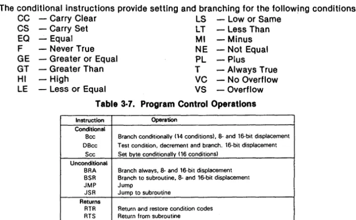
INTERRUPTS
The DIMENSION 68000 comes with six maskable levels of interrupts and one non-maskable interrupt level. The maskable interrupt levels are le-vels 1, 2, 3, 4, 5, and 6. The non-maskable interrupt level is level 7. Levell is the lowest priority and level 7 is the highest priority. The DUART (which is described above) is set by the hardware circuitry to be the non-maskable interrupt on priority level 7. The DUART has the capa-bility to mask for interrupts the Keyboard, the RS-232, the printer, and the Real Time Clock. All of the interrupts on the DIMENSION 68000 utilize the Autovector type of interrupt processing.
The Autovector processing computes the interrupt vector number (in hex) by the following formula:
VECTOR NUMBER
=
(PRIORITY-LEVEL + 024)The above formula gives the interrupt vector number in hexadecimal. The Autovector processing computes the location of the interrupt vector (in hex) by the following formula:
VECTOR LOCATION
=
VECTOR NUMBER*
4Page 28 VERSION 0.00
The location of the vector address contains the address of an inter-rupt routine. The following chart shows the assignments for priority level, vector number, and vector address for the DIMENSION 68000.
PRIORITY VECTOR LOCATION OF
DEVICE LEVEL NUMBER VECTOR ADDRESS
(decimal) (decimal) (hex)
---
---
---
---SLOT 6 1 25 064
SLOT 5 2 26 068
SLOT 4 3 27 06C
SLOT 3 4 28 070
SLOT 2 5 29 074
SLOT 1 6 30 078
DUART 7 31 07C
Additionally, there are exception vectors. Vectors 0 and 1 are taken as a pair and not as two separate vectors. The following chart shows the assignments for the vector number, the vector address, and its usage.
VECTOR NUMBER (decimal) 2 3 4 5 6 7 8 9 10 11 12 - 24 32 - 255
MEMORY
VECTOR
ADDRESS ASSIGNMENT (hex) 000 004 008 00C 010 014 018 0lC 020 024 028 02C 030-060 080-3FF
Reset: Initial Supervisor Stack pointer Reset: Initial Program Counter
Bus Error Address Error Illegal Instruction Zero Divide
CHK Instruction TRAPV Instruction Privelege Violation Trace
Line 1010 Emulator Line 1111 Emulator NOT USED
NOT USED
USED BY
BOOT CP/M CP/M CP/M CP/M CP/M CP/M CP/M CP/M CP/M CP/M NO USER NO USER
The DIMENSION 68000 memory is byte addressable. Each memory address has associated with it an additional bit that is used for emulation trap-ping. If a memory address is accessed, and the emulation trap bit is on, then the emulation strobe bit, on the bus and at the slots, is tog-gled.
The DIMENSION 68000 can address up to 16 MBytes of memory. This is made possible by the use of a 24 Bit wide address.
VERSION 0.00 Page 29
The DIMENSION 68000 memory has, in its associated circuitry, bus arbi-tration logic. The bus arbiarbi-tration priorities are:
HIGHEST
LOWEST
CRT CONTROLLER CIRCUITRY EXPANSION SLOT 6
EXPANSION SLOT 5 EXPANSION SLOT 4 EXPANSION SLOT 3 EXPANSION SLOT 2 EXPANSION SLOT I MC68000 CPU
EXPANSION SLOTS
Each EXPANSION SLOTS can accept a plug in card. Each slot directly con-nects to the system's bus. A detailed discussion of the connections for the EXPANSION SLOTS is contained in the EXPANSION SLOT PINOUT APPENDIX.
Each EXPANSION SLOT has four signals that are unique to that slot. They are:
- BOARD ENABLE - BOARD REQUEST - BOARD ACKNOWLEDGE - BOARD INTERRUPT
FROM SYSTEM
TO SYSTEM
FROM SYSTEM
TO SYSTEM
The Micro Craft Corporation supplies an expansion slot board prototyp-ing kit. This kit contains a prototypprototyp-ing board, a set of expansion slot board drawings, data regarding the signals available on the expansion slot connector, and data about the DIMENSION 68000 system circuitry.
CO-PROCESSORS
The DIMENSION 68000 has been designed to allow the simultaneous use of more than one processor. All of the emulator cards have a microproces-sor chip on them. This makes all of the emulator cards, co-processors. Some other possible co-processor uses are:
- an array processor
- a mathematical floating point processor - a mathematical multiply and divide processor - a specific machine emulator
- an intelligent device controller
Page 3fcJ VERSION 0.00
VERSION 0.00 Page 31
C HAP T E R 3
M E M 0 R Y ALL 0 CAT ION
SYSTEM REFERENCE MANUAL CHAPTER 3
VERSION 0.00 Page 33
MEMORY CIRCUITRY
The MEMORY CIRCUITRY contains bus arbitration logic circuitry and emu-lation trapping circuitry. The bus arbitration logic circuitry is de-signed to give to the CRT Controller circuitry the highest priority. The next highest priority to EXPANSION SLOT 6, then, EXPANSION SLOTS 5, 4, 3, 2, and 1. The lowest priority is the MC68000 CPU.
The emulation trapping circuitry for the memory is implemented by in-cluding in the memory design an additional bit with each byte of mem-ory. The additional bit is used as an emulation trapping flag. If the bit is on for a specific byte, and that byte is accessed, then the emu-lation circuitry causes the emuemu-lation strobe bit in the system bus to be pulsed. This does NOT hold true for accesses by the CRT Controller circuitry, NOR does it hold true for accesses by the MC68000 CPU.
MEMORY MAP
The DIMENSION 68000 memory contains both Read Only Memory (ROM) and Random Access Memory (RAM). The system memory is allocated as follows.
ADDRESS FUNCTION
************ 000000 000004 000008 00000C 000010 000014 000018 0000lC 000020 000024 000028 00002C
INTERRUPT VECTORS ****************************************
RESET - Initial Stack Pointer
000030 - 00005F 000060 000064 000068 00006C 000070 000074 000078 00007C
000080 - 0000BF 0000C0 - 0000FF
RESET - Initial Program Counter (PC) BUS ERROR
ADDRESS ERROR ILLEGAL INSTRUCTION DIVIDE BY 0
CHECK INSTRUCTION TRAPV INSTRUCTION PRIVILEGE INSTRUCTION TRACE
OPCODE 1010 EMULATION OPCODE 1111 EMULATION Reserved
SPURIOUS INTERRUPT LEVEL 1 INTERRUPT LEVEL 2 INTERRUPT LEVEL 3 INTERRUPT LEVEL 4 INTERRUPT LEVEL 5 INTERRUPT LEVEL 6 INTERRUPT
LEVEL 7 INTERRUPT - DUART - Keyboard, printer, etc. TRAP VECTORS
Reserved
Page 34 VERSION 0.00
ADDRESS FUNCTION
************
PERIPHERAL CONTROLLER BOOT RAM***************************
000100 - 000113 CONTROLLER 1
000114 - 000127 CONTROLLER 2
000128 - 00013B CONTROLLER 3
00013C - 00014F CONTROLLER 4
000150 - 000163 CONTROLLER 5
000164 - 000177 CONTROLLER 6
************
RESERVED PERIPHERAL RAM**********************************
000178 - 00019B MONITOR RESERVED LOCATIONs
00019C TOP OF RAM
0001A0 - 0001A7 ADDRESS of ROM BASED RESET VECTOR 0001A8 - 0001CB CRT PARAMETER TABLE
0001CC - 0001E5 BOOT DISK PARAMETER TABLE 0001E6 - 0001E9 SYSTEM CONFIGURATION WORD 0001EA - 0001ED ADDRESS of TEXT SCREEN TABLE 0001EE - 0001Fl ADDRESS of KEYBOARD TABLE
0001F2 - 0001F5 ADDRESS of GRAPHICS CHARACTER SET #1 TABLE 0001F6 - 0001F9 ADDRESS of GRAPHICS CHARACTER SET #2 TABLE 0001FA - 0001FD ADDRESS of PRESENT SCREEN TABLE
0001FE INTERRUPT MASK FOR 2861 I/O CHIP
0001FF END OF RESERVED PERIPHERAL RAM
************
USER RAM AREA********************************************
000200 - 00119F NORMAL (80 x 50) SCREEN TEXT AREA 001200 - 01FFFF MINIMUM SYSTEM USER RAM
001300 Start of CP/M-68K TRANSIENT PROGRAM AREA
010000 - 01FFFF Co-Processor RAM Area, During Emulation (Min) 010000 - 07FFFF Co-Processor RAM Area, During Emulation (Max) 020000 - FEFFFF Expanded User RAM Area
************
RESERVED AREAS*******************************************
FF0000 - FFIFFF Basic Processor ROM Area (ROMBIOS and MONITOR) FF2000 - FF7FFF Reserved Area (Graphics RAM)
************
INPUT/OUTPUT REGION**************************************
FF8000 - FF87FF CRT Controller
FF8800 - FF8FFF Slot I FF9000 - FF97FF Slot 2 FF9800 - FF9FFF Slot 3 FFA000 - FFA7FF Slot 4 FFA800 - FFAFFF Slot 5 FFB000 - FFB7FF Slot 6
FFB800 - FFBFFF Reserved
FFC000 - FFC3FF Reserved
FFC400 - FFC7FF Keyboard/Printer/Modem/Real Time Clock
FFC800 - FFCBFF Speaker
FFCC00 - FFCFFF Game Control
FFD000 - FFD3FF Floppy Disk
FFD400 - FFD7FF Emulation Controller
FFD800 - FFDBFF Reserved
FFDC00 - FFDDFF ROM Toggle
FFDE00 - FFDFFF Reserved
FFE000 - FFFFFF Reserved
VERSION 0.00 Page 35
USES
The USES for the DIMENSION 68000 system memory are described by the a-bove memory map. Some of the descriptions will be further amplified here.
The area from FF0000 to FF1FFF comprise the ROMBIOS area. This name is a combination of ROM and BIOS, where BIOS is short for Basic Input / Output System. The ROMBIOS provides the routines for I/O and for the DIMENSION 68000 system MONITOR. The MONITOR is a collection of routines that are used to "boot" the system and to communicate with the Keyboard and the CRT.
Each interrupt vector is a location in memory that contains the address of a software routine (or a ROMBIOS routine) that handles the interrupt that is associated with that specific location. The interrupt vectors are used by CP/M, by the EXPANSION SLOTS, and by the DUART which han-dles the Keyboard, the Printer Port, the RS-232 Interface, and by the Real Time Clock.
The highest address of the RAM varies depending on the amount of RAM that is installed. The following chart shows the relationship between the amount of memory installed and the highest address in RAM.
AMOUNT HIGHEST
OF MEMORY
MEMORY ADDRESS
---
---128 KB 01FFFF
256 KB 02FFFF
384 KB 03FFFF
512 KB 04FFFF
16 MB FEFFFF
Page 36 VERSION 0.00
VERSION 0.00 Page 37
C HAP T E R 4
c
P / M - 6 8 K , C P M B lOS , AND ROM B lOSYERSIOM 0.00 Page 39
FLOW
The CP/M-68K operating system is basically composed of three parts; the Console Command Processor (CCP), the Basic Disk Operating System (BOOS), and the Basic Input / Output System (BIOS). The CCP handles the commands that are typed in from the console (or are entered from a sub-mit file) such as DIR, or SUB.
The BOOS handles the functions such as file access, drive system/program control, and exceptions. The BOOS partially character Input/Output (I/O) functions.
access, handles
The largest part of the character I/O handling and .all of the basic I/O handling is performed by the CP/M BIOS. The CP/M BIOS accesses the I/O functions that are provided in the DIMENSION 68000 Read Only Memory BIOS (ROMBIOS). The ROMBIOS actually controls the I/O controllers and I/O devices.
The CP/M operating system is described more fully in the CP/M-68K Oper-ating System User's Guide and it the CP/M OperOper-ating System Programmer's Guide. Both manuals are from Digital Research, Inc. Digital Research, Inc., is the company that developed CP/M and it is the company that li-censes the use of CP/M.
ADDITIONAL CALLS
There is a list of the CP/M-68K functions in the Programmer's Guide. The Micro Craft Corporation tional functions to the CP/M-68K operating system SIaN 68000 computer. The additional functions are lowing pages.
SYSTEM REFERENCE MANUAL
CP/M Operating System has added three addi-for use on the DIMEN-presented in the
Page 40 VERSION 0.00
FUNCTION 256: Change Diskette Drive Format
Entry Parameters: Register D0.W Register Dl.W
=
Register D2.W
Returned Values: NONE
CHAPTER 4
l00H
=
256 (decimal) New Disk Drive Unit Number where 0 Drive A:1 Drive B: 2 Drive C: 3 Drive D: 4 Drive E: 5 Drive F: 6 Drive G: 7 Drive H: New Disk Drive Format where 0 null
1 Std 40 track 2 Std 80 track
3 IBM single side (CPM 86) 8 sector 4 IBM double side (CPM 86) 8 sector 5 TRS 80
6 Kaypro
7 Cromemco
8 Osborne
9 IBM 3740 8 Inch Single Side, Density A TRS 16 Double Side, Density
B User Defined
VERSION 0.00 Page 41
FUNCTION 257: Read Diskette Drive Format Entry Parameters:
Register De.W Register Dl.W
=
Returned Values:
lelH
=
257 (decimal) Disk unit Number where 13 Drive A:1 Drive B: 2 Drive C: 3 Drive D: 4 Drive E: 5 Drive F: 6 Drive G: 7 Drive H:
Register De.W
=
Selected Drive Type where 13 nullSYSTEM REFERENCE MANUAL
1 Std 413 track 2 Std 813 track
3 IBM single side (CPM 86) 8 sector 4 IBM double side (CPM 86) 8 sector 5 TRS 813
6 KayPro 7 Cromemco 8 Osborne
9 IBM 37413 8 Inch Single Side, Density A TRS 16 Double Side, Density
B User Defined
Page 42 VERSION 0.00
FUNCTION 258: Set the Physical Parameter Table, Set the CP/M Disk Parameter, or Set the Disk Interlace Table
Entry Parameters:
Register D0.W l02H
=
258 (decimal) Register Dl.W=
Command Selectwhere 0 Ignore
1 Set Physical Parameters (DPRMTX 16 words)
2 Set CP/M Disk Parameter Block Table
(DPBX 8 words)
3 Set Interlace Table (XLTX 64 words) Register D2.L = Table Address
Returned Values: NONE
YERSION 0.00 Page 43
TERMINAL ATTRIBUTES
The DIMENSION 68000 CP/M BIOS has been augmented to provide a set of "ESCAPE SEQUENCES" that will handle various screen functions on the CRT display. Also, several "CONTROL" screen functions have been implemen-ted. The following charts list the "ESCAPE SEQUENCES" and the "CONTROL" functions. These functions are accessed by outputting the code or codes through the CP/M "CONOUT" function.
CONTROL FUNCTIONS
HEX
VALUE FUNCTION
---Bl Clear Screen
07 Bell
B7 Home
91 Cursor Up
92 Cursor Left
93 Cursor Right
94 Cursor Down (Line Feed)
ESCAPE SEQUENCES (Escape plus the hex value listed)
HEX ASCII
VALUE CODE FUNCTION
- - - -
---48 H Home Cursor
3D position Cursor
76 v Clear Screen & Home Cursor
41 A Cursor Up
42 B Cursor Down
43 C Cursor Right
44 D Cursor Left
4B K Erase End of Line
4A J Erase End of Page
78 x Clear End of Line
79 y Clear End of Page
63 c Turn On Cursor Flag
64 d Turn Off Cursor Flag
65 e Turn On Inverse Flag
66 f Turn Off Inverse Flag
page 44 VERSION 0.00
ROMBIOS
The CP/M functions operate by performing calls to the appropriate rou-tines in the ROMBIOS. ROMBIOS is an acronym for the ROM Based Input / Output System. The usage of the ROMBIOS is fully described in the ROM-BIOS Appendix to this manual. A chart showing the ROMBIOS functions is included to illustrate the contents of the ROMBIOS.
ROMBIOS FUNCTIONS
1 Initialize CRT Controller
2 Output a character to the screen 3 Clear the TEXT screen
4 Read a key stroke 5 Get keyboard status 6 Boot from disk
7 Start the built-in monitor 8 Read selected disk drive status 9 Select disk drive and turn motor ON 10 Deselect disk drive and turn motor OFF 11 Seek to selected disk track
12 Seek to track 0 and recalibrate disk rezero 13 Seek to track and read a sector
14 Seek to track and write a sector 15 Seek to track and format a track 16 Format the entire disk
17 Read the sector ID information 18 Read the disk status
19 Reserved 20 Reserved
21 Read Printer Status
22 Output a character to Printer Interface 23 position CRT cursor
24 Read character at present CRT cursor location 25 Clear Graphics Screen
26 Set graphics color 27 Plot X, Y point 28 Reserved
29 Read color at designated point
30 Output Character to CRT with No Control Characters
YERSIOM 0.00 Page 45
INPUT / OUTPUT
To fully appreciate the functions supplied in the ROMBIOS, requires a knowledge of the actual input and output circuitry used inside the DIM-ENSION 68000 computer. A detailed discussion of the programming re-quirements for the input and the output circuitry is included in the DIRECT I/O Appendix to this manual.
Page 46 VERSION 0.00
'ERStOIl 0.00 Page 49
C HAP T E R 5
C P / M - 6 8 K
VERSION 0.00 Page 51
BDOS AND BIOS
The CP/M operating system is composed of two parts; the Basic Disk Op-erating System (BDOS) and the Basic Input / Output System (BIOS). The BDOS is that part of the operating system that is independent of the Input/Output.
The BIOS is that part of the operating system that is concerned with Input/Output. The BIOS for the DIMENSION 68000 system uses the ROMBIOS as much as is possible. The CP/M BIOS includes a table that handles diskettes and also handles the RS-232 port. The label that has been as-signed to that table is "drivetb". Following is a description of the "drivetb" table.
TABLE OFFSETS
OFFSET +0 +1 +2 +3 +4 +5 +6 +7 +8 +9 +10 +11 +15 +16 +17 +20 +21 +22 +24 +26 +28 +32 LENGTH
1 byte 1 byte 1 byte 1 byte 1 byte 1 byte 1 byte 1 byte 1 byte 1 byte 1 byte 4 bytes 1 byte 1 byte 4 bytes 1 byte 1 byte 2 bytes 2 bytes 2 bytes 4 bytes 4 bytes
DESCRIPTION
Number of Disk types
DUART reset RS-232 command DUART select RS-232 command DUART set 9600 bits per second DUART set no parity/8 bits DUART set normal/l stop bit RS-232 XON/XOFF flag
Old Track Number
Old Physical Sector Number New Track Number
New Sector Number New DMA Address Old Disk Unit Retry Count
Save Location for the Dl register Save Location
Save Location Drive
Warm Boot Flag
Number of Memory Regions
=
1Starting Address of the Memory Region(s) Ending Address of the Memory Region(s)
Page 52 VERSION 0.00
ADDITIONAL CALLS
The DIMENSION 68000 version of CP/M has three functions added to the normal CP/M calls. The functions are:
256 - Change Diskette Drive Format
Entry Parameters: Register D0.W Register Dl.W ='
Reg i ster D2. t-v
Returned Values: Register D0.W
100H
=
256 (decimal)New Disk Drive unit Number where 0 Drive A:
1 Drive B: 2 Drive C: 3 Drive D: 4 Drive E: 5 Drive F: 6 Drive G: 7 Drive H: New Disk Drive Format where 0 null
1 Std 40 track 2 Std 80 track 3 IBM single side 4 IBM double side 5 TRS 80
6 Kaypro
7 Cromemco
8 Osborne
9 IBM 3740 8 Inch Single Side, A TRS 16 Double Side, Density B User Defined
257 - Read Diskette Drive Format
Entry Parameters: Register D0.W Register Dl.W
=
Retruned Values: Register D0.W
101H
=
257 (decimal) Disk Unit Number where 0 Drive A:1 Drive B: 2 Drive C: 3 Drive D: 4 Drive E: 5 Drive F 6 Drive G 7 Drive H
Density
YERSION 0.00
258 - set the Physical Parameter Table, Set the CP/M Disk Parameter, or Set the Disk Interlace Table
Entry Parameters:
Register D0.W 102H
=
258 (decimal) Register Dl.W=
Command Selectwhere 0 Ignore
1 Set Physical Parameters (DPRMTX 16 words)
Page 53
2 Set CP/M Disk Parameter Block Table
(DPBX 8 words)
3 Set Interlace Table (XLTX 64 words) Register D2.L Table Address
Returned Values: Register D0.W
TERMINAL ATTRIBUTES
The DIMENSION 68000 CP/M BIOS has been augmented to provide a set of "ESCAPE SEQUENCES" that will handle various screen functions on the CRT display. Also, several "CONTROL KEY" screen functions have been imple-mented. The following charts list the "ESCAPE SEQUENCES" and the "CON-TROL KEY' functions.
CONTROL KEYS
---HEX KEYS TO
VALUE PRESS FUNCTION
- - - -
---Bl Alt 1 Clear Screen
07 Fa 'Bell
B7 Alt 7 Home
91 Alt End 1 Cursor Up
92 Alt Own 2 Cursor Left
93 Alt Pgd
:3
Cursor Right94 Alt Lft 4 Cursor Down (Line Feed)
[image:57.475.53.428.58.244.2]Page 54 VERSION 0.00
To generate the escape code (27Hex) press CTRL plus the '" key ESCAPE SEQUENCES (Escape plus the key value listed)
HEX VALUE 48 3D 76 41 42 43 44 4B 4A 78 79 63 64 65 66 USAGES
KEYS TO PRESS H v A B C D K J x Y c d e f FUNCTION Home Cursor position Cursor
Clear Screen & Home Cursor Cursor Up
Cursor Down Cursor Right Cursor Left Erase End of Line Erase End of Page Clear End of Line Clear End of Page Turn On Cursor Flag Turn Off Cursor Flag Turn On Inverse Flag Turn Off Inverse Flag
The CP/M call that is used to "Change Diskette Drive Format" is one of the functions that is used by the "RESET" utility program to set the disk formats. The additional calls that have been added to the
DIMEN-SION 68000 CP/M system are accessed in the same way as the standard CP/M function calls.
VERSION 0.00
Backup BASIC
Central Processor
I N D E X
Connecting Dimension Together Connectors
Copy CP/M-68K
Creating Backup Disks CRT
Cursor DIMENSION
Disk Drive Configurations Disk Drive Expansion Disk Test
Emulators 6512 8086 Z80
Expansion Slots Firmware
Formatting New Disks FORTRAN 77+
Installation Checklist I/O Devices
Keyboard Languages Location
Making Disk Copies MC68000L8
Monitor Motherboard OFF/ON Switch Power
Power Supply Assembly Program Loading RESET Switch ROMBIOS Startup System unit Test
Unpacking VDU
SYSTEM REFERENCE MANUAL
Page X-I
VERSION 0.00 Page A-l
A P PEN 0 I X A
The T O O L - K I T
VERSION 0.00 Page A-3
Some users of the DIMENSION 68000 require detailed information on the circuitry, on the software used in the CP/M BIOS, or on the software used in the ROMBIOS. For these users, the Micro Craft Corporation pro-vides a "Tool-Kit" that contains the following items:
- A complete set of the schematic diagrams for the Main Printed Circuit Board of the DIMEMSION 68000 computer.
- A diskette that contains the following items:
- A copy of the source code for the CP/M BIOS.
- A copy of the source code for the ROMBIOS.
The Micro Craft Corporation wishes to encourage other parties that wish to manufacture equipment for the DIMENSION 68000. In order to provide that encouragement, the Micro Craft Corporation will license the use of the design information for the DIMENSION 68000 and the software used in the DIMENSION 68000. The license for this use will be ROYALTY FREE.
To arrange for a license for the use of the design information and the software for the DIMENSION 68000, contact the Micro Craft Corporation at the following address.
MICRO CRAFT CORPORATION OEM SALES
4747 IRVING BLVD. DALLAS, TX. 75247
Also, all purchasers of the "Tool-Kit" will be notified of any updates to the software or major changes to the hardware. Copies of these chan-ges will be made available to the purchasers of the "Tool-Kit" for a small SHIPPING AND HANDLING FEE.
page A-4 VERSION 0.00
VERSION 0.00 Page A-5
If your application for the DIMENSION 68000 requires any of
the following items:
- A copy of the schematic diagram - A copy of the listing for the ROMBIOS - A copy of the listing for the CP/M BIOS
These items are available from the Micro Craft Corporation as
"The Tool-Kit" for $99.95 (Residents of Texas add 6 % sales
tax). To order "The Tool-Kit", please sign the attached
Non-Disclosure Agreement, fill out and mail this form.
- - - F 0 L D HER E - - -
-Name _______________________________________ Title __________________ _
Company __________________________________________________________ __
Address __________________________________________________________ __
City ___________________________________ State __________ zip ________ __
Telephone _______ ) ______________________________________________ __
- - - F 0 L D HER E - - -
-I certify that -I will hold as confidential, all proprietary
information that I receive from Micro Craft Corporation, and
will not divulge that information to anyone without written
permission, nor use that inform,ation for any purpose not in
the best interests of the Micro Craft Corporation.
Date Signature
Page A-6
MICRO CRAFT CORPORATION CUSTOMER SERVICE DEPARTMENT 4747 IRVING BLVD.
DALLAS, TX. 75247
VERSION 0.00
VERSION 0.00 Page B-1
A P PEN D I X B
DIM ENS ION KEYBOARD COD E S
KEYBOARD CODES
YERSION 0.00 Page B-3
KEY B OAR D COD E S
Un- Cntl/ Alt Alt Alt
Key shift shft Cntl Shft Alt shft Cntl Cnt/Shft
A 61 41 Cl Cl El Cl Cl Cl
B 62 42 C2 C2 E2 C2 C2 C2
C 63 43 C3 C3 E3 C3 C3 C3
D 64 44 C4 C4 E4 C4 C4 C4
E 65 45 C5 C5 E5 C5 C5 C5
F 66 46 C6 C6 E6 C6 C6 C6
G 67 47 C7 C7 E7 C7 C7 C7
H 68 48 C8 C8 E8 C8 C8 C8
I 69 49 C9 C9 E9 C9 C9 C9
J 6A 4A CA CA EA CA CA CA
K 6B 4B CB CB EB CB CB CB
L 6C 4C CC CC EC CC CC CC
M 6D 4D CD CD ED CD CD CD
N 6E 4E CE CE EE CE CE CE
0 6F 4F CF CF EF CF CF CF
P 70 50 D0 D0 F0 D0 D0 D0
Q 71 51 Dl Dl Fl Dl Dl Dl
R 72 52 D2 D2 F2 D2 D2 D2
S 73 53 D3 D3 F3 D3 D3 D3
T 74 54 D4 D4 F4 D4 D4 D4
U 75 55 D5 D5 F5 D5 D5 D5
V 76 56 D6 D6 F6 D6 D6 D6
W 77 57 D7 D7 F7 D7 D7 D7
X 78 58 D8 D8 F8 D8 D8 D8
Y 79 59 D9 D9 F9 D9 D9 D9
z
7A 5A DA DA FA DA DA DAl ! 31 21 31 21 Bl Al Bl Al
2@ 32 40 32 C0 B2 C0 B2 C0
3# 33 23 33 23 B3 A3 B3 A3
4$ 34 24 34 24 B4 A4 B4 A4
5% 35 25 35 25 B5 AS B5 A5
6" 36 5E 36 DE B6 DE B6 DE
7& 37 26 37 26 B7 A6 B7 A6
8* 38 2A 38 2A B8 AA B8 AA
9 ( 39 28 39 28 B9 A8 B9 A8
0) 30 29 30 29 B0 A9 B0 A9
KEYBOARD CODES
Page B-4 VERSION 0.00
Un- Cntl/ Alt Alt Alt
Key shift Shft Cntl Shft Alt Shft Cntl Cnt/Shft
2D 5F DF DF AD DF DF DF
=+ 3D 2B 3D 2B BD AB BD AB
[ { 5B 7B DB DB DB FB DB DB
] } 5D 7D DD DD DD FD DD DD
,
-60 7E 60 7E E0 FE E0 FE
,
.
3B 3A 3B 3A BB BA BB BAI " 27 22 27 22 A7 A2 A7 A2
\1
5C 7C DC DC DC FC DC DC,<
2C 3C 2C 3C AC BC AC BC.>
2E 3E 2E 3E AE BE AE BE/? 2F 3F 2F 3F AF BF AF BF
SPC 20 20 20 20 A0 A0 A0 A0
INS-0 10 0A E0 E0 90 8A E0 E0
DEL-. 8B 0B 7F 7F 8B 8B FF FF
END-l 11 0C BE BE 91 8C BE BE
DWN-2 12 0D FE FE 92 8D FE FE
PGD-3 13 0E BF BF 93 8E BF BF
LFT-4 14 0F AC AC 94 8F AC AC
5 15 lA BA BA 95 9A BA BA
RGT-6 16 IB BB BB 96 9B BB BB
HOM-7 17 lC FB FB 97 9C FB FB
UP-8 18 ID FD FD 98 9D FD FD
PGU-9 19 IE FC FC 99 9E FC FC
2D 2D 2D 2D AD AD AD AD
+ 2B 2B 2B 2B AB AB AB AB
RTRN CD CD CA CA CD CD CA CA
BKSPC C8 C8 7F 7F C8 C8 FF FF
ESC DB DB DB DB DB DB DB DB
BRK 8C 8D 8D 8D 8C 8D 8D 8D
PRT-* 2A IF BC BC AA 9F BC BC
TAB C9 AA AB AB C9 AA AB AB
ENTR 8A 8A 8A 8A 8A 8A 8A 8A
VERSIOM 0.00 Page B-5
Un- Cntl/ Alt Alt Alt
Key shift Shft Cntl Shft Alt Shft Cntl Cnt/Shft
Fl 00 A0 9A 9A 80 A0 9A 9A
F2 01 Ai 9B 9B 81 Ai 9B 9B
F3 02 A2 9C 9C 82 A2 9C 9C
F4 03 A3 9D 9D 83 A3 9D 9D
F5 04 A4 9E 9E 84 A4 9E 9E
F6 05 A5 9F 9F 85 A5 9F 9F
F7 06 A6 AE AE 86 A6 AE AE
F8 07 A7 AF AF 87 A7 AF AF
F9 08 A8 8E 8E 88 A8 8E 8E
F10 09 A9 8F 8F 89 A9 8F 8F
KEYBOARD CODES
Page B-6 VERSION 0.00
VERSION 0.00 Page C-l
A P PEN D I X C
A S C I I COD E S
YERSION 0.00 Page C-3
American Standard Code for Information Interchange
A S C I I C H A R A C T E R S E T
7
-
B I T C a D E )MSD 0 1 2 3 4 5 6 7
000 001 010 011 100 101 110 I I I
LSD
I
---+---+---+---+---+---+---+---+---0 ---+---+---+---+---+---+---+---+---0---+---+---+---+---+---+---+---+---0---+---+---+---+---+---+---+---+---0---+---+---+---+---+---+---+---+---0 NUL DLE SP 0 @ P P
1 0001 SOH DC1 1 A Q a q
2 0010 STX DC2 II
2 B R b r
3 0011 ETX DC3 # 3 C S c s
4 0100 EaT DC4 $ 4 D T d t
5 0101 ENQ NAK % 5 E U e u
6 0110 ACK SYN & 6 F V f v
7 0111 BEL ETB 7 G W g w
8 1000 BS CAN ( 8 H X h x
9 1001 HT EM ) 9 I Y i y
A 1010 LF SUB
*
J Z j zB 1011 VT ESC
+
K [ k {C 1100 FF FS
<
L \ 1D 1101 CR GS M ] m
E 1110 SO RS
>
N nF 1111 SI US / ? 0 0 DEL
Page C-4 VERSION 0.00
YERSIOII 0.00 Page D-l
A P PEN D I X D
E X PAN S ION S LOT
PIN 0 U T
VERSION 0.00 Page D-3
EXPANSION SLOT PINOUT
The following illustration identifies the pin locations and pin signa-tures of the ~dge connectors (*
=
Low TRUE signal, 0VDC).CONNECTOR
Vee 1 2 Vee +5VDC +,- 1%
Vee
-
- 3 4 -Vee @ lA Max/PinRST* 5 6 R/W* (slot max 3A)
MEMCYC* 7 8 CRTREQ*
D0 9 10 Dl
D2 11 12 D3
D4 13 14 D5
Data Bus D6 15 16 D7
D8 17 18 D9
D10 19 20 Dll
D12 21 22 D13
D14 23 24 D15
LOWC* 25 26 DRSEL1*
Disk 2SIDE* 27 28 HLOAD*
Drive Exp. INDEX* 29 30 HEAD*
Cnt'l STEP* 31 32 DIRC*
WENA* 33 34 WDATA*
RDATA 35 36 TK00*
DRSEL0* 37 38 WPROT*
LDS* 39 40 ACK0*
DISPEN* 41 42 E
INTRP* 43 44 EMULATION STROBE
VMA* 45 46 HLT*
Fl 47 48 F2
(A0) UDS* 49 50 F0
A22 51 52 A23
A20 53 54 A21
A18 55 56 A19
A16 57 58 A17
Address Bus A14 59 60 A15
A12 61 62 A13
A10 63 64 All
A8 65 66 A9
A6 67 68 A7
A4 69 70 AS
A2 71 72 A3
-12 VOLTS - 73 74 Al
Sl-6* 75 76 ACKl-6*
+12 VOLTS 77 78 +12 VOLTS
INTl-6* - 79 80DATAVAL*
14.31818 MHz 81 82 BDl-6ENA*
GROUND 83 84 GROUND
GROUND 85 86 GROUND
Page 0-4 VERSION 0.00
EXPANSION SLOT PIN DESCRIPTIONS
The following text descr'ibes the function of each Expansion Slot pin. The number, located in front of the abbreviation and pin signature identifies which pin (or group of pins) is being described. Asterisks, located behind a pin signature, indicate signals that are low when true
(0VDC) •
1 - 4 vcc
5
6
7
8
9 - 24
PINOUT
+5 VDC +,- 1% @ 1 Amp Max/-~n 3 Amps Max per Expansion Slot (6.5 Amps tOtd~ for 6 slots)
RST* System Master Reset (0.1VDC typical) Power On Reset 200 milliSeconds minimum
Reset Button 200 milliSeconds minimum
68000 RESET Inst 128 CPU clock Cycles
(approximately 17.8 micro-Seconds)
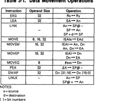
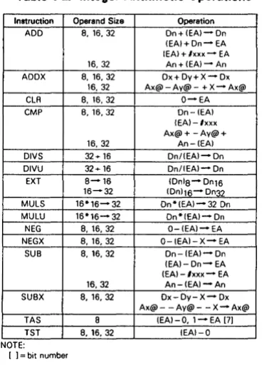
R/W* READ/WRITE * (t