ABSTRACT—A backside layout design for multiple cell RCIGBT is proposed to suppress the snapback effect which happens in the turn-on process of RCIGBT in this paper. The internal operation mechanism of RCIGBT has been analyzed by device simulation, proving that our backside layout design works well. Reduction in the ratio of backside N+/P+ area as well as the N buffer doping density and increase in the number of cells in chip are all proved as useful methods in reducing snapback voltage. Although some novel RCIGBT structures have been proposed to eliminate the snapback effect, most of them have been based on a single cell structure, which is not sufficient for the analysis of RCIGBT. It’s more practical and feasible in production to simply optimize the backside layout design of N+, P+ short area with the multiple cell RCIGBT structure. Here we will report on the analysis of the snapback effect and the backside optimum layout design for the multiple cell RCIGBT.
Index Terms—backside layout, multiple cell, RCIGBT, snapback
I. INTRODUCTION
The RCIGBT(reverse-conducting insulated gate bipolar transistor) is a promising kind of power devices, which can replace the pair of an IGBT chip and a free wheeling diode chip in some conversion circuits by one. Also it can flow larger current than the VDMOS. However, the snapback effect is a common problem in the turn on process of RCIGBT, which has a bad influence on the performance of circuits.
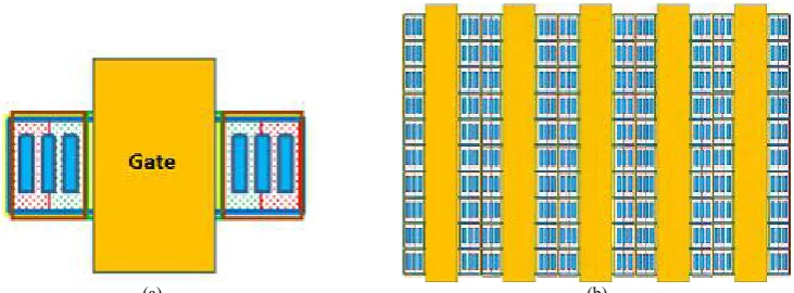
In this paper, we propose a novel and practical backside layout design, taking the multiple cell structure of RCIGBT into consideration, as shown in Fig. 1(b). The results of simulation clarify that our design can achieve snapback-free with simpler fabrication process comparing with other structure designs based on a single cell, which will be helpful in production.
[image:1.595.117.483.396.531.2](a) (b)
Fig. 1. Top view of RCIGBT chip (a)Single cell structure (b)Multiple cell structure
Manuscript received January 08, 2019; revised January 23, 2019. The experiments of this work were supported by Kitakyushu Science and Research Park Semiconductor Center.
Zhongke. Chang is with Graduation School of Information, Production, and Systems, Waseda University, Japan (phone: 080-2671-5877; fax: 093-692-5021; e-mail: colin_007@ toki.waseda.jp).
Xiaofei. Zhu was with Graduation School of Information, Production,and Systems, Waseda University, Japan. (e-mail: [email protected]).
Masahide. Inuishi is with Graduation School of Information, Production,and Systems, Waseda University, Japan. (e-mail: [email protected]).
II. STRUCTURE ANDMECHANISM
The operating mechanism of RCIGBT in the forward mode can be divided into two modes generally. In Fig. 2, the P body, the N-drift region and the P+ collector form a PNP bipolar transistor. Rchis the channel resistance. Rjis the the junction FET resistance. Rn-driftis the the drift region resistance. And RCSis the equivalent collector short resistance which impedes electrons to flow from the drift region to the N+ collector short. Ieand Ihare the electron current and the hole current. In Fig. 2(a), the voltage between the base and the emitter is low. PNP bipolar transistor is in the OFF state. There is only electron current flowing through the device. RCIGBT works in the MOS mode. With the increase of collector voltage, RCIGBT turns into the IGBT mode like Fig. 2(b). Holes in the P+ collector are injected into the N-drift region and the PNP bipolar transistor turns on. The conductivity modulation of the drift region causes the significant reduction of the Rn-drift, which leads to a snapback in voltage[1]. VSBis the collector voltage when snapback
Backside Layout Design of Snapback-free
RCIGBT with Multiple-Cell
effect happens. Vpnis the build-in potential between backside P+ short and N-drift or backside P+ short and N-buffer[2].
[image:2.595.125.452.83.243.2](a) (b)
Fig. 2. Forward mode of RCIGBT (a)MOS Mode (b)IGBT Mode
Fig. 3 shows the snapback effect in the I-V characteristics of RCIGBT.
pn CS
CS drift -n j ch
SB R V
R R
R R
V (1)
Fig. 3. Snapback effect of RCIGBT
III. SIMULATION ANDANALYSIS
Refer to (1), there are four factors Rch, Rj, Rn-driftand RCS, which can be adjusted to suppress the snapback effect. Rch, Rj and Rn-driftare mainly determined by the MOSFET structure and the doping concentration of the wafer while RCSmainly depends on the backside layout.
A. Reducing Rchand Rj
By extending the distance between two P bodies in each cell or reducing the lateral channel length under the gate, we can obtain smaller Rjand Rch, leading to smaller VSB.
Since the carrier density is also influenced by the P-body distance and the channel length after the device turns into the IGBT mode, even though we can reduce VSB, ΔVSBkeeps almost the same.
B. Reducing Rn-drift
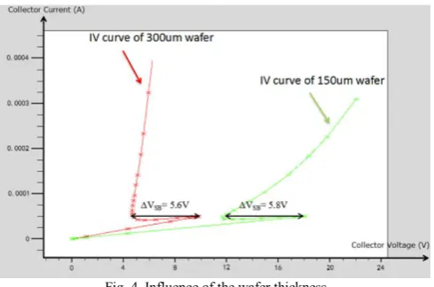
By reducing the wafer thickness or using the carrier stored layer(CS layer)[3] under the P body, the conductivity modulation[4] by the injection of carriers into the N-drift region can be enhanced. As a result, we can obtain smaller
[image:2.595.305.550.460.622.2]ΔVSB(5.6V) of RCIGBT on 150um wafer is almost the same as that(5.8V) of RCIGBT on 300um wafer.
Fig. 4. Influence of the wafer thickness
C. Increasing RCS
simulation.
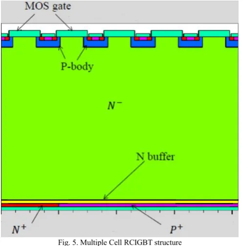
Fig. 5. Multiple Cell RCIGBT structure
Table. I gives the parameters used for the multiple cell RCIGBT in device simulation.
As shown in Fig. 6, when the number of the top cells increases while the ratio of backside N+/P+ area is kept constant as 1:1, VSBis reduced from 100V(2 cells), 50V(3 cells) to 18V(5 cells). Also ΔVSB is reduced from 77V(2 cells), 32V(3 cells) to 7V(5 cells).
Once the gate is turned on and high voltage is applied to the collector, the initial electron current flows from the
N-emitter to the backside N+ short, passing through the N-drift region above the collector. We can regard the travelling path of electrons inside the N-drift region as two dimensions: vertical and lateral. Actually, the lateral distance along which the initial electron current flows increases with increase in the number of the top cells, as shown in Fig. 7. In this way, RCS increases, resulting in the reduction of the snapback effect.
In the same principle, reducing the ratio of backside N+/P+ short area can also suppress the snapback effect[5].
Fig. 6. Influence of the number of cells on snapback voltage(N buffer doping=5×1016cm-3)
Fig. 7 shows the backside N+ short placed at the one side of the chip instead of in the middle position. With this layout design, the total lateral travelling distance of electron currents from each channel will be the maximum. Consequently the snapback effect can be completely eliminated as shown in Fig. 8.
[image:3.595.307.549.182.333.2]Surrounding the IGBT area with reverse diode area on the backside of the chip will be an economical and practical snapback-free method.
[image:3.595.55.285.451.655.2]Fig. 7. Electron Current distribution TABLE I
DEVICE SPECIFICATIONS
Parameter Value
Wafer thickness 300 um
N-drift doping density 11014cm-3(Phosphor) N-drift width for each cell 82 um
N-buffer thickness 1 um P-body width for each cell 21 um
P-body depth 10 um
P-body doping density 51016cm-3(Boron) Backside N+ short thickness 1 um
Backside N+ short doping density 11020cm-3(Phosphor) Backside P+ short thickness 1 um
Backside P+ short doping density 11020cm-3(Boron) N-emitter thickness 1 um
N-emitter doping density 11020cm-3(Phosphor) P-emitter thickness 1 um
P-emitter doping density 11020cm-3(Boron) Gate oxide thickness 50 nm
[image:3.595.304.547.484.663.2]Fig. 8. I-V characteristics when N+ short is at side(N buffer doping=1×1017cm-3, ratio of backside N+/P+ width=1:3)
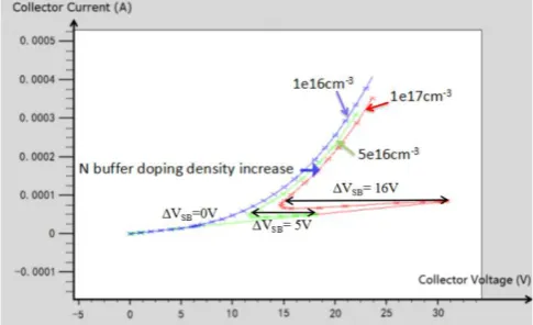
In Fig. 9, VSBis reduced from 32V(1×1017cm-3), 17.5V(5× 1016cm-3) to 0V(1 × 1016cm-3) with the decrease of the N-buffer doping density. Also ΔVSBis reduced from 16V(1× 1017cm-3), 5V(5×1016cm-3) to 0V(1×1016cm-3).
The N-buffer, commonly used to increase the breakdown voltage, also affects the snapback voltage. With increase in the N-buffer doping density, the breakdown voltage of the vertical device will increase. Taking the trade-off relationship of breakdown voltage and snapback voltage into consideration, it is required to optimize the N-buffer doping
density.
Fig. 9. Influence of the N-buffer doping density (ratio of N+/P+=1:1, N+ in the middle of backside, N-buffer doping=1×10¹⁶, 5×10¹⁶, 1×1017cm-3)
IV. EXPERIMENT ANDRESULTS
We have designed several kinds of backside layout for RCIGBT chip. Fig. 10 shows some of our backside masks which will be used in the fabrication process. In Fig. 10, the whole backside active area of the chip is covered by the N+ short and the P+ short. The ratio of N+/P+ area are 1:9, 1:3 and 1:1 respectively with N+ area at one side of the chip and in the middle of the chip.
[image:4.595.305.548.75.223.2](a) (b) (c) (d)
Fig.10. Backside masks for N+/P+ short area with Gate
[image:4.595.57.539.368.499.2](a)N+ area at side & N+/P+=1:9 (b)N+ area at side & N+/P+=1:3 (c)N+ area in the middle & N+/P+=1:3 (d)N+ area in the middle & N+/P+=1:1
Fig. 11 shows the fabricated wafer. device chip, reduction in the ratio of the backside N+/P+short area and decrease in the N-buffer doping density within limit. However, optimizing the relative positions of backside N+/P+ shorts is a more practical way for the production.
Novel RCIGBT structures like AB RCIGBT, TFP RCIGBT, and DFS RCIGBT[6-12] have been proposed to realize snapback-free RCIGBT. But the multiple cell structure should be taken into consideration when we analysis and evaluate the characteristic of the RCIGBT.
REFERENCES
[image:4.595.48.276.542.694.2][4] A. Barna, D. Horelick, “A Simple Diode Model Including Conductivity Modulation” in IEEE Transections on Circuit Theory, Vol 18, No. 2, March 1971.
[5] H. Jiang, B. Zhang, W. Chen, Z. Li, C. Liu, Z. Rao and B. Dong, “A Snapback Suppressed Reverse-Conducting IGBT With a Floating p-Region in Trench Collector” in IEEE Electron Device Letters, Vol, 33, No. 3, March 2012.
[6] J. Wei, X. Luo, L. Huang, B. Zhang, “Simulation Study of a Novel Snapback-Free and Low Turn-Off Loss Reverse-Conducting IGBT With Controllable Trench Gate” in IEEE Electron Device Letters, Vol, 39, No. 2, February 2018.
[7] L. Storasta, M. Rahimo, M. Bellini, A. Kopta, U. R. Vemulapati, N. Kaminski, “ The Radial Layout Design Concept for the Bi-mode Insulated Gate Transistor ” in Proceedings of the 23rd International Symposium on Power Semiconductor Devices & IC’s, May 2011. [8] L. Zhu, X. Chen, “A Novel Snapback-Free Reverse Conducting IGBT
with Anti-parallel Shockley Diode ” in Proceedings of the 25th International Symposium on Power Semiconductor Devices & IC’s. [9] M. Takahashi, D. Hofmann, S. Yoshida, A. Tamenori, Y. Kobayashi,
O. Ikawa, “Extended Power Rating of 1200V IGBT Module with 7G RC-IGBT Chip Technologies” in PCIM Europe 2016, May 2016. [10] Takuya Yoshida, “ The Second-generation 600V RC-IGBT with
Optimized FWD” in Proceedings of the 26th International Symposium on Power Semiconductor Devices & IC’s, June 2016.
[11] L. Zhu, X. Chen, “An Investigation of a Novel Snapback-Free Reverse-Conducting IGBT and With Dual Gates” in IEEE Transaction On Electron Devices, Vol. 59, NO. 11, November 2012.