warwick.ac.uk/lib-publications
Original citation:
Hamilton, Dean P., Jennings, Michael R., Pérez-Tomás, Amador, Russell, Stephen A. O.,
Hindmarsh, Steven A., Fisher, Craig A. and Mawby, P. A. (Philip A.). (2016) High temperature
electrical and thermal aging performance and application considerations for SiC power
DMOSFETs. IEEE Transactions on Power Electronics. doi: 10.1109/TPEL.2016.2636743
Permanent WRAP URL:
http://wrap.warwick.ac.uk/84556
Copyright and reuse:
The Warwick Research Archive Portal (WRAP) makes this work by researchers of the
University of Warwick available open access under the following conditions. Copyright ©
and all moral rights to the version of the paper presented here belong to the individual
author(s) and/or other copyright owners. To the extent reasonable and practicable the
material made available in WRAP has been checked for eligibility before being made
available.
Copies of full items can be used for personal research or study, educational, or not-for profit
purposes without prior permission or charge. Provided that the authors, title and full
bibliographic details are credited, a hyperlink and/or URL is given for the original metadata
page and the content is not changed in any way.
Publisher’s statement:
© 2016 IEEE. Personal use of this material is permitted. Permission from IEEE must be
obtained for all other uses, in any current or future media, including reprinting
/republishing this material for advertising or promotional purposes, creating new collective
works, for resale or redistribution to servers or lists, or reuse of any copyrighted component
of this work in other works.
A note on versions:
The version presented here may differ from the published version or, version of record, if
you wish to cite this item you are advised to consult the publisher’s version. Please see the
‘permanent WRAP url’ above for details on accessing the published version and note that
access may require a subscription.
Manuscript received June 6, 2016. D. P. Hamilton is with the University of Warwick, Coventry, CV4 7AL, United Kingdom (phone: +44 2476-151382; fax: +44 2476-418922; e-mail: [email protected]).
1.University of Warwick, Coventry, CV4 7AL, United Kingdom. *Corresponding author 2.Catalan Institute of Nanoscience and Nanotechnology, Bellaterra, Barcelona, Spain
Abstract— the temperature dependence and stability of three different commercially-available unpackaged SiC DMOSFETs have been measured. On-state resistances increased to 6 or 7 times their room temperature values at 350 °C. Threshold voltages almost doubled after tens of minutes of positive gate voltage stressing at 300 °C, but approached their original values again after only one or two minutes of negative gate bias stressing. Fortunately, the change in drain current due to these threshold instabilities was almost negligible. However, the threshold approaches zero volts at high temperatures after a high temperature negative gate bias stress. The zero gate bias leakage is low until the threshold voltage reduces to approximately 150 mV, where-after the leakage increases exponentially. Thermal aging tests demonstrated a sudden change from linear to non-linear output characteristics after 24 to 100 hours air storage at 300 °C and after 570 to 1000 hours in N2 atmosphere. We attribute this to nickel oxide growth on the drain contact metallization which forms a heterojunction p-n diode with the SiC substrate. It was determined that these state-of-the-art SiC MOSFET devices may be operated in real applications at temperatures far exceeding their rated operating temperatures.
Index Terms—Power MOSFETs, Temperature measurement, Aging, Oxygen, Insulated gate bipolar transistors
I. INTRODUCTION
ILICON Carbide power MOSFET devices have now been commercially-available for more than six years. Full SiC power modules incorporating SiC Schottky barrier diodes and SiC MOSFETs were also made available shortly after. Other types of SiC power devices like BJT and JFET have also been commercialized but, in general, have seen less commercial success and, in some cases, discontinued. One of the perceived main advantages of the SiC devices is their potential to operate at much higher temperatures than silicon power devices like IGBTs. In fact, SiC devices are intrinsically capable of operating at very high temperatures and are actually manufactured using very high melting temperature
materials. Their performance and reliability of commercially-available devices under such conditions is therefore of interest but there have been relatively few independent studies done on this to date. In this paper, the first two generations of SiC MOSFET devices have been evaluated to obtain their electrical and thermo-mechanical performances at temperatures up to 350 °C. The target application for this is a high performance hybrid electric vehicle inverter whose junction temperature is allowed to increase up to a peak of approximately 300 °C for occasional short distances, such that the space and weight consuming cooling system does not have to be scaled up to meet this occasional demand. Although 350 °C is approximately 200 °C above the rated operating temperatures of current SiC MOSFET devices, initial static measurements showed good performance up to 350 °C, beyond which device failures were noted.
The materials used in the manufacture of these devices are well known, and known to be capable of being operated well above the rated device temperatures – the only question is how long. To illustrate this point, a SiC PiN diode made from a similar material set has already demonstrated very good electrical performance up to 900 °C, at least for the duration of the measurements [1]. The purpose of this present work was to evaluate the readiness of the commercially-available devices for high temperature applications and, in particular, to determine how they degrade and how long they last.
Another author has reviewed the possible roles for SiC devices and concluded that they would be unlikely to find much use until they are able to operate at ambient temperatures exceeding 300 °C and that the limitation for long term high temperature reliability is the metal-semiconductor ohmic contact [2]. Thermal cycling above such temperatures would also make the long-term hermetic sealing of the packaging a challenge, therefore the real test for these devices is long-term operation in air. For these reasons, and because there are no
High temperature electrical and thermal aging
performance and application considerations for
SiC power DMOSFETs
Dean P. Hamilton
1*, Michael R. Jennings
1,
Member, IEEE
, Amador Pérez-Tomás
2, Stephen. A. O.
Russell
1, Steven A. Hindmarsh
1, Craig. A. Fisher
1and Philip A. Mawby
1,
Senior
Member, IEEE
long term reliable die on substrate encapsulation materials available for such high temperatures, high temperature aging tests have also been carried out on bare die in air in this work, as well as in an inert atmosphere. The impact of the oxygen penetration on the rate of degradation of the electrical characteristics of these SiC MOSFETs has been obtained so that the remaining lifetime of the devices can be incorporated into a whole system lifetime model.
The reliability of the ohmic contacts at high temperatures has received a great deal of attention, both in air atmosphere and inert atmospheres. For example, the degradation mechanisms of contacts of semiconductors in general, including at high temperatures, were summarized to be due to diffusion and subsequent formation of solid solutions or compounds [3]. The inter-diffusion can increase the contact resistance by orders of magnitude, and compound formation can induce coefficient of thermal expansion (CTE) mismatch, brittleness and open circuits. The degradation mechanisms of ohmic contacts for SiC at high temperatures was shown by [4], and can be summarized as voiding due to dissimilar diffusion rates of adjacent metal layers. In the case of operation in air or oxygen containing environments, various metal stack and ceramic oxygen diffusion barriers have been demonstrated on top of the ohmic contacts to have high performance at extremely high temperatures from 450 °C to 750 °C [5-10]. It is not known whether such features have been incorporated into commercially-available devices, as such detail is generally retained as commercial secrets by the device manufacturers.
A number of other authors have already demonstrated the performance of SiC devices at high temperatures. SiC JFETs capable of operating for thousands of hours at 500C have been demonstrated [11]. Commercially-available versions of so-called SiC Junction Transistors have also been shown to operate well up to 500 °C [12] and have demonstrated current gains higher than 60 at 350 °C, roughly half of their room temperature gain [13]. For SiC DMOSFETs, the temperature dependence of drain-source current, mobility, channel resistance and threshold voltage (VT) up to 300 °C was comprehensively demonstrated by [14]. The threshold voltage was shown to have a negative temperature dependence. The high temperature performance of SiC JFETs and DMOSFETs up to 300 °C has also been partially studied by [15], where it was shown that transconductance of SiC DMOSFETs increases with temperature while the threshold voltage decreases with temperature. This has the effect of reducing the channel resistance and counteracting the positive temperature dependence of the drift region resistance to keep the overall on-state resistance (RDS,ON) relatively temperature insensitive. Their results demonstrated a two-fold increase in RON,SP from room temperature to 300 °C. It was also suggested that the SiC JFET is more suitable for high temperature operation due to its lower drain-source leakage at high temperatures, and because there is no channel resistance.
One of the perceived main negative issues of SiC DMOSFET devices is the threshold voltage drift under positive and
negative gate bias temperature stress conditions (simultaneous high gate bias and high temperature for long time periods). This was anticipated to have been solved in second generation devices. However, this has already been shown not to be the case for temperatures above their rated maximum operating temperatures [16, 17]. It was shown that the VT shift is still significant for plastic packaged devices when operated at 225°C, especially for an extreme constant negative gate voltage of -20V, which is significantly below the normal -5V limit of today’s commercially-available devices. It was suggested that the negative bias causes a greater shift because holes are more susceptible to oxide trapping than electrons. This trapping is known to be extremely fast process, as has been demonstrated by [18]. The temperature dependence of interface trapping and temperature on VT has also been illustrated mathematically and used to demonstrate its sensitivity to the P-well doping concentration for practical values of VT around +2V [19]. Most importantly, the possibility of the device becoming normally on at high temperatures was also discerned. Another author has demonstrated the positive benefit of using a constant negative gate bias at up to 250 °C, by showing that it decreases the drain-source leakage current significantly [17], but only at the expense of increased negative threshold voltage drift. The impact of switched gate bias temperature stressing, as opposed to constant gate bias, was also demonstrated by the same author to emulate the real application conditions. An initial and significant VT drift of between -150 mV to -350 mV was demonstrated after the first 30 minutes of operation (with no intermediate measurements), followed by a slow drift of approximately 1 - 2 mV per hour. One of the only other authors to study the effects of physical degradation of SiC MOSFET devices demonstrated electrical failure of the devices due to gate dielectric erosion and disconnection of the ohmic contacts after 32 hours at 500 °C [20].
In almost all of the previous works highlighted, the authors demonstrated the performance of a single and mostly proprietary device under a limited set of conditions and, in some cases, had a direct affiliation with the device manufacturer. In this paper, two different widely available SiC DMOSFET devices from the current second generation and one device from the first generation, for comparison, are evaluated independently for their high temperature performance and thermo-mechanical reliability. These new results complement the existing results and are presented in a way that demonstrates the state of the art, rather than to identify which manufacturer has the best product. These results will also serve as a benchmark for a future evaluation of the third generation devices that are now just becoming available.
II. EXPERIMENTAL PROCEDURE
output characteristics, threshold voltage drift, drain current leakage and reverse breakdown voltages. Approximately fifteen of each type have undergone thermal aging in air or inert atmospheres and some have been subjected to
temperature cycling tests. The three MOSFET types were all rated at 1.2 kV, approximately 30 A continuous drain current at room temperature and with a surface area in the order of 10 to 15 mm2.
A. High temperature electrical measurements
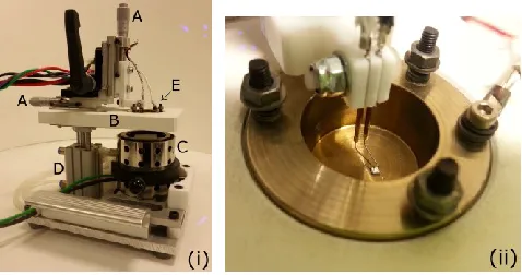
A heated probe station was designed and manufactured to evaluate the electrical performance of the devices, as shown in Fig. 1. The devices, in bare die form, were tested individually by placing the drain terminal side down in the polished stainless steel container. This container was lowered onto the hotplate for testing, with voltage isolation to the heater provided by a thin aluminum nitride (AlN) disk. The gate and source terminals were probed by specially designed high temperature capable tungsten rhenium S-bend probes that had good elasticity to facilitate the application of pressure to the die topside aluminum metallization. For high temperature reverse breakdown tests, a dielectric fluid capable of being heated to 300 °C for periods of a few minutes was poured into the container. The electrical measurements were conducted using a Tektronix 371B curve tracer and the measured characteristics were saved as images and spreadsheet files. Calibration exercises were first carried out to determine the safe electrical limits for single-shot and sweep measurements using the curve tracer, to avoid device damage and significant self-heating up to the maximum temperature. In general, this meant limiting the maximum drain current to around 5 A. A new die was used for every high temperature test, to eliminate the possibility of additional measurements being influenced by the stresses caused by previous high temperature measurements. More than fifty die were tested for their high temperature electrical performance in total. Differential on-state resistance measurements were taken from the slope of the output characteristics as measured by the curve tracer. Gate threshold voltage measurements were conducted on the curve tracer by connecting the gate and drain terminals (VDS = VGS), setting the gate-drain voltage limit and then performing a single-shot pulsed measurement. The threshold voltage was read from the resulting plot of VDS = VGS versus current at 20
µA. This current was chosen to be well above the threshold voltage knee, and low enough to prevent a positive threshold voltage shift during the measurement, and during additional measurements. The curve tracer was connected to the heated die probe station for all of these measurements. Gate bias temperature stressing was performed by connecting the heated probe station to a laboratory power supply with the drain and source terminals connected together. The zero volt and drain-source connections were exchanged to apply the negative gate bias stress.
B. High temperature storage tests
Approximately fifty new die have also been used for these aging tests. Aging in air was carried out by placing the die on a laboratory ceramic hotplate, drain side down, for a fixed period of time up to 100 hours storage time. For the aging in inert atmosphere, the die were placed on a thin aluminum oxide sheet in a tube furnace with an N2 gas flow rate of approximately 1.4 slm for 1000 hours storage in total. In all cases, the sets of devices were periodically removed, cooled quickly in air by placing them on a large block of polished aluminum, and then were electrically tested using the curve tracer. Typically, the output characteristics and threshold voltage were recorded in this case, before returning them to the high temperature environment to continue the aging tests.
III. RESULTS
A. On-state resistance measurements
In order to facilitate the calculation of conduction losses and scale the cooling system performance up to the high temperatures of interest in this work, the drain to source on-state resistance RDS,ON of the devices have been measured up to 350 °C. This temperature was chosen as the limit for testing because the failure rate appeared to increase quickly above this temperature. The results of the RDS,ON measurements are shown in Fig. 2, normalized to their room temperature starting values, which were all between approximately 80 mΩ and 100 mΩ. These values are close to the manufacturer data sheet values up to their 150 °C ratings, increasing to approximately two times their room temperature values, but increasing more rapidly with temperature thereafter. This is expected to be because the ratio of channel to drift resistance has been optimized to be close to the maximum rated operating temperature of the devices, which are all 150 °C, and above which the channel resistance is decreasing slightly slower than the drift resistance is increasing. It can be seen that, for the SiC MOSFETs under test, RDS,ON has increased to 6 or 7 ± 1 times their room temperature values at 350 °C. The error bars also show the large spread of values for different die of the same type.
B. High temperature instability of threshold voltage
During electrical testing at the high temperatures, instability of the gate threshold voltage (VT) was noted for some of the devices; VT was increasing while carrying out the higher temperature electrical measurements. Fig. 3 illustrates this variation for a small number of slow heating and cooling cycles of the probe station hot plate while carrying out pulsed
[image:4.612.47.286.53.179.2]
I-V measurements using the curve tracer. These results clearly illustrate significant instability for one device type, and good stability for the other from a different manufacturer for this single-shot pulsed measurement scenario. The resulting VT instability shown for the SM1 device type is due to the combination of temperature dependence and drift due to the curve tracer pulsed gate bias temperature stress. For the SM2 device, the temperature dependence is similar, but the VT instability is negligible. Gate bias switching tests have been carried out by a previous author who suggested that constant gate bias conditions, used by other researchers and in this work, are not realistic and under realistic switching conditions the VT drift will be negligible [21]. However, the results shown in Fig. 3 and those of other authors [16, 17] prove that the drift
can be affected by switched operation, especially above the device’s rated temperatures, but it will always be a strong function of the switching frequency and duty ratio. A previous study on older SiC MOSFET devices used a ramped gate bias
turn-on and demonstrated VT instability even at room temperature, and which increased when the gate voltage was ramped up more quickly [22]. However, the constant bias conditions give a good measure of device VT stability and have therefore been used for the remainder of the present work.
1) Instability due to bias temperature stressing
[image:5.612.64.287.50.238.2]Gate bias temperature stressing (BTS) was carried out to quantify the extent of the observed threshold voltage drifts at 300 °C by applying +20 V gate bias voltage for 30 minutes followed by -5 V gate bias for 30 minutes. These values are the maximum gate-source voltages for the devices under test. The measured results shown plotted in Fig. 4 show a near two-fold threshold voltage increase for the positive gate bias pBTS tests for two of the three SiC MOSFET types. These two SiC MOSFET devices, labelled SM1 and SM3, are first and second generation devices from the same manufacturer, which indicates that no significant improvement in the threshold voltage instability has been achieved by that manufacturer.
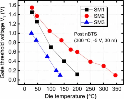
Fig. 5. Post nBTS temperature dependence of threshold voltage VT following
the 30 minute -5 V nBTS test period at 300 °C. These results illustrate the situation that could occur if VT drifts too far in a negative direction; the
[image:5.612.323.552.51.239.2]devices may enter a normally-on state.
Fig. 3. Measured threshold voltage VT versus die (top) surface temperature
for two different SiC MOSFET types and for a small number of hotplate heating and cooling cycles. The arrows indicate the order of single-shot pulsed measurements during temperature cycling.
Fig. 4. SiC MOSFET threshold voltage VT measured for the three different
device types before and after BTS testing for 30 minutes at 300 °C, and for +20 V and -5 V gate biases. All VT measurements were taken at room
temperature and for a drain current of 20 µA.
Fig. 2. Normalised temperature dependence of on-state resistance RdsON
[image:5.612.68.275.287.460.2] [image:5.612.334.545.292.461.2]The results also indicate that, within the same time period, this increase, or VT drift, can be completely corrected by the negative gate bias nBTS stress. Interestingly, the VT drift due to pBTS was almost negligible for the SM2 device type, which is a second generation device from a different manufacturer. This suggests that the SM2 devices have a much lower density of near interface traps (NITs) and-or oxide traps than the other two devices, most probably due to its specific SiO2 growth conditions. In general, a relatively low spread of measured values was found for all device types for the initial room temperature VT measurements and a larger spread was found for the devices following the high temperature BTS tests. This indicates a strong material variation in the thermally generated density of near interface traps or oxide traps from die to die.
2) Temperature dependence
The temperature dependence of threshold voltage for the three device types is also shown in Fig. 5, for the worst case situation where the threshold voltages have been permanently reduced by the high temperature negative gate bias nBTS tests. The shift will be permanent unless a positive bias or a further period of negative bias is applied later at an elevated
temperature. It can be seen from these results that the threshold voltages all have a negative temperature dependence, which approaches zero volts at relatively low temperatures for two device types but not until almost 350 °C for the SM2 type device. This is partly due to the fact that the SM2 device has a lower VT temperature dependence of approximately 4 mV / °C than the other two device types whose temperature dependence is approximately 8 mV / °C, and partly because the SM2 devices have less drift at constant negative bias and therefore had the highest room temperature VT values at the start of these tests. These VT temperature dependencies were found to be identical for any other VT starting values.
3) Time dependence
The time and temperature dependence of VT drift due to both maximum positive gate bias and minimum negative gate bias has also been obtained for one device type, as shown in Fig. 6. In this case, the temperature and maximum positive gate bias were applied and VT was measured for different periods up to a total of 2 hours, after which the maximum negative gate bias of -5 V was applied. All measurements were taken after cooling down to room temperature, and every
Fig. 9. Measured drain-source leakage currents versus die temperature for three different SiC MOSFET types, measured at Vds = 10 V, Vgs = 0 V. The associated room temperature threshold voltage values (VT,RT) are also shown.
The leakage levels are heavily dependent on VT,RT and increase exponentially
[image:6.612.331.548.49.201.2]when VT ≤ 150 mV approximately.
Fig. 7. Temperature dependence of maximum threshold voltage VT drift and
time to reach 90 % of this maximum under constant bias BTS test conditions for the SM3 type devices.
Fig. 8. Representative measured output characteristics for the three different SiC MOSFET types before and after the +20 V pBTS and -5 V nBTS constant gate bias stress tests at 300 °C for 30 minutes. Measurements were taken at room temperature and Vgs = +20 V.
[image:6.612.68.268.54.206.2]
Fig. 6. Time dependence of threshold voltage VT drift under constant bias
BTS test conditions for SM3 type devices. A positive gate bias was applied for up to 2 hours followed by negative bias for up to 45 minutes. Measurements were taken after cooling to room temperature.
[image:6.612.332.545.246.406.2] [image:6.612.74.273.256.421.2]measurement point is taken from a separate new device that has not been previously stressed (this removes the possibility of new measurements being influenced by previous measurements). The results clearly demonstrate the time dependence of the VT drift which increases relatively slowly before rolling off to a maximum for the constant positive gate bias temperature stress. However, the VT drift decreases extremely rapidly for the negative gate bias temperature stress, with VT returning to its starting value or lower in one or two minutes. This negative bias VT drift is also referred to by some authors as negative bias temperature instability (NBTI). At low temperatures, the VT drift is low, almost negligible. However, as the temperature is increased the threshold shifts higher, but the time dependence of the VT drift appears to be relatively independent of temperature for both the positive and negative gate bias. This situation is illustrated better in Fig. 7 where the maximum VT drift and time to reach 90 % of the maximum are plotted against temperature. It can be seen from this that the maximum drift increases significantly as the device is heated, but slows down sharply and rolls off at 250 °C. These results also demonstrate that it takes longer to reach 90 % of the maximum VT drift value as the temperature of the device is increased, and has a near linear temperature dependence. This temperature dependence is approximately 280 ms.K-1, or, can be stated as a heating rate (β) of approximately 15 K.s-1. It is worth noting that these test conditions are the worst case situations for these devices; using the maximum rated positive and negative gate voltages. Although it would be desirable to use the maximum possible positive gate voltage to extract maximum current from each device, it might be possible for some lower-noise applications to use a value for the negative gate bias closer to zero volts. The benefits in terms of negative bias temperature instability, which of course would result in a lower VT drift have recently been demonstrated by another author for a proprietary SiC DMOSFET where the drift was demonstrated to be approximately four times less for a -1 V gate bias than for a – 5 V bias over a 1000 second period [23].
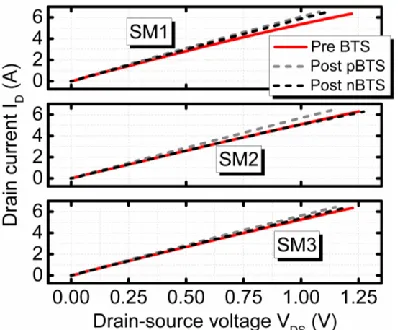
4) Impact on drain current
It is important to know how much the stresses that cause these threshold voltage drifts effect the drain current (Id) up to high temperatures so that the devices can be de-rated sufficiently in the real application. The output characteristics have been measured for the three device types before and after the 30 minute BTS stress tests at 300 °C, and up to approximately 6 Amperes. As can be seen from the representative results shown in Fig. 8, the change in current is almost negligible for this current range, despite the quite high threshold voltage shifts reported in Fig. 4. The measured VT values for the results shown pre-BTS, after pBTS and after nBTS tests respectively for these specific die were SM1: 1.75, 4.1, 1.1; SM2: 1.5, 1.85, 1.4; SM3: 1.6, 2.25, 0.95 V. However, this negligible change in drain current after BTS tests was found for all die tested.
5) Drain-source leakage current
The drain–to-source leakage current and its temperature dependence are shown in Fig. 9 for all three device types along with the associated threshold voltage measurements for each measurement temperature. It can be seen from these
measurements that the leakage current is very low, in the order of 4 μA to 8 μA, for the entire measured temperature range of almost 350 °C in some cases. It is clear from these results that there is a very strong dependence of leakage current on the room temperature value of the threshold voltage VT. For example, an SM1 type device with high VT value of 3.65 V displays low leakage up to almost 350 °C. However, an SM1 device type with an extremely low VT of 1.05 V shows an exponential increase at temperatures higher than
approximately 125 °C. This is happening because VT is already low and approaches zero volts at a relatively modest temperature due to its strong negative temperature
dependence. The same situation exists for the SM3 device type results. It appears from these results that the leakage begins to increase exponentially if VT is reduced to below approximately 150 mV within the operating temperature range. In general, these results demonstrate that this occurs for devices with high drift like the SM1 and SM3 devices, even when their room temperature VT values are relatively high, or devices with low VT drift like the SM2 devices even with their low room temperature VT values.
C. Output characteristics before and after aging
Aging experiments were carried out by placing a number of die in high temperature storage at 300 °C in both air and inert N2 atmospheres. The air storage experiments were carried out by heating the die, placed drain side down, on a ceramic hotplate. The temperature of the hotplate cycled slowly up and down by no more than ±5 °C, presumably as a result of its thermostatic control. The inert atmosphere storage tests were carried out using a laboratory tube furnace. The precise temperature and temperature variation inside the tube furnace is unknown, but is expected to be small enough to neglect.
1) Air atmosphere aging
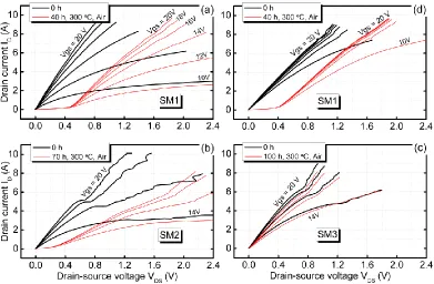
linear even after 100 hours of storage in air, and with a comparably smaller RDS,ON increase of 21 % (from 96 mΩ to 115 mΩ). The measurements shown in Fig. 10 (a-b) were all conducted at room temperature. The same SM1 device was also measured at 150 °C, before and after air storage, as shown in Fig. 10(d); in this case, the on-state resistance has increased by 70 % (from 121 mΩ to 207 mΩ). The transconductance (gm) has also increased at this elevated measurement temperature, particularly at the lower gate voltages. We attribute this gm increase to the approximately 1 V reduction in threshold voltage at 150 °C which, according to the standard transconductance equation for a power DMOSFET, would give a 10 % increase in gm for Vgs = 10 V but only a 5 % increase at Vgs = 20 V. These results also indicate that the
knee voltage for the non-linear response of device type SM1 has decreased from approximately 400 mV at room temperature to 250 mV when measured at 150 °C, comparing (a) to (c) and projecting along the resistance slopes to the X-axis intersects. The room temperature knee value for the SM2 device is even lower at approximately 220 mV. Fig. 10(e) plots the temperature dependency of the air storage aging process for the SM1 device type for 6 h measurement intervals. These results confirm that the transformation from a linear to non-linear output characteristic does occur quite suddenly; in this case after between 12 h and 18 h approximately, and the transformation appears to be complete after approximately 40 h. There is also a gradual increase in the on-state resistance from 0 h to 200 h, which seems to be
Fig. 10. (a-d) Measured linear region output characteristics for the three different SiC MOSFET types before after aging in air for storage periods up to 100 hours at 300 °C. Vgs was increased in 2 V steps up to +20 V and all measurements were taken at room temperature except (d) which was measured at 150 °C in order to illustrate the temperature dependence before and after aging. These measurements were taken after 0 h, 40 h, 70 h for SM2 and SM3 die only and 100 h for the SM3 die only.
Fig. 10 (e) Aging time period dependence of the output characteristics for up to 196 hours to illustrate the change versus aging time a long time after the rectifying output becomes evident. (f) Threshold voltage shifts due to aging in air at 300 °C for up to 100 hours. In this case, single-shot measurements were taken carefully to limit the possibility of further measurement pulses influencing the results.
[image:8.612.113.504.51.307.2] [image:8.612.61.552.363.518.2]independent of the occurrence of the non-linear characteristic. Fig. 10(f) shows the measured threshold voltage versus air storage aging period for all three device types. The only significant shift was found for the SM1 device type. Further work is required to determine whether this shift is due to the aging process, or is simply an accumulation of trapped charges due to the multiple periodic measurements.
2) Temperature cycling in air
A number of SM1 type die were also temperature cycled in a thermal cycling chamber with air atmosphere. It was found that these die had the same electrical characteristics before and after 1000 temperature cycles from 0 °C to 350 °C, with no non-linearity. In this case, the thermal cycling profile spends approximately 5 minutes per cycle above 300 °C, for a total of 83 hours, and 15 minutes per cycle below 300 °C. This situation is curious because all of the devices aged in air at a constant temperature of exactly 300 °C showed the non-linear output characteristics after less than 40 continuous hours. The reasons for these differences are under investigation. However, it appears from these results that the cumulative time period above 300 °C is not equivalent to a continuous period.
3) N2 atmosphere aging
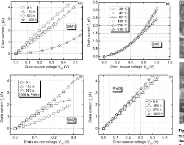
The results for our inert atmosphere aging at 300 °C are shown in Fig. 11 for the three device types. In these cases, the SM1 type device aged in N2 showed a slightly non-linear characteristic at the 1000 hour measurement point, but not after 570 hours (no measurements were taken in-between). In
contrast to the air storage results where the SM1 devices degraded before the SM2 devices (after 40 h and 70 h respectively), the inert storage results showed the opposite order; the SM2 device type had the non-linear output characteristic at the 570 hour measurement point. Unfortunately, this SM2 device was not functional after 1000 hours for reasons unknown. In common with the air-aged die, the SM3 device type produced the normal MOSFET linear output characteristic after 1000 hours in N2 storage. The appearance of the non-linear responses, even in this inert N2 atmosphere, but only after approximately ten times the durations for devices stored in air, strongly suggests that the N2 atmosphere did contain some small amount of oxygen. The actual levels of oxygen in this laboratory tube furnace are currently under investigation.
4) Validation of non-linear output characteristic theory
Our assumption about the possible presence of a (p-type) nickel oxide adjacent to the n-type SiC substrate has been validated by milling trenches in the drain contact at various positions on the die surface using a focused ion beam (FIB) system, an example of which is shown in Fig. 12(a). The associated SEM image of the drain contact metallization stack on the sidewall and energy dispersive X-ray (EDX) elemental analysis revealed the formation of a continuous layer of nickel oxide on top of the nickel diffusion barrier, under the surface of the silver back metallization as shown in Fig. 12(b).
Fig. 12. (a) Tilted surface SEM image of one of a number of FIB trenches milled in the drain side of the SM2 die after heating for 1000 hours in N2. (b)
Cross section SEM image of drain contact metallization stack taken from the FIB trench sidewall, indicating the formation of a nickel oxide layer under the silver.
Fig. 11. (a-c) Measured linear region output characteristics versus inert N2 atmosphere storage period at
[image:9.612.398.563.49.297.2] [image:9.612.47.411.50.336.2]IV. DISCUSSION
The operation of these SiC MOSFETs up to at least 300 °C has been shown to be feasible in this work, even for extended periods in air. However, we have demonstrated that the high temperature environment produces high levels of on-state resistance and VT instability that will have to be considered carefully in the system design of a real high temperature power converter. We have also introduced a new issue in this work; the time-dependent thermal aging of these SiC MOSFET devices when oxygen is present at high temperatures, such as might be the case if the packaging hermetic seal eventually fails.
A. The consequences and management of VT instability
It is likely that the next generations of devices will still have the problem of gate threshold voltage instability (or drift) to some degree, at least when operated at very high temperatures, and for both positive and negative gate bias. It would be difficult and expensive to monitor and correct the threshold voltage drift in a real system, mostly because the device turn-on and off times are so fast (in the order of tens of nanoseconds). Both a positive and negative high temperature bias stress would be needed to correct the drift if VT were to be monitored. The question then arises about how and if it can be managed for real high temperature applications, or not.
1) Positive BTS instability solution
We have demonstrated the VT instability for positive gate bias, including for a switched bias, and shown that the VT increase can be significant at high operating temperatures. However, we have also demonstrated that, despite this large shift, the impact on the drain current appears to be almost negligible, and the amount of VT drift is limited and dependent on the highest operating temperature. In our opinion then, this positive shift, although undesirable, can be easily tolerated and compensated for if thought necessary as part of the current de-rating strategy for the whole system.
2) Negative BTS instability solution
The constant negative gate bias presents a particular problem; we have demonstrated that a large negative gate bias produces large and extremely rapid negative drifts of the threshold voltage when operated at high temperatures. These drifts are cumulative but have been shown in this work to be limited in magnitude and can be counteracted by a high temperature positive gate bias stress. However, such large negative shifts, when coupled with the negative temperature dependence of the threshold voltage, make the possibility of the threshold voltage approaching zero volts, or potentially much lower, a realistic possibility even at modest temperatures as was demonstrated in Fig. 5. The most likely scenario where large negative threshold voltage drifts could occur in a real application is if a converter operation is stopped temporarily while operating at very high temperatures, and halting the switching operation by holding all the SiC MOSFET devices off with a high e.g. maximum negative gate bias. When switching operation resumes and the device junction temperatures rise again, the device threshold voltages will
decrease even further due their negative temperature coefficients. It is feasible that, for some SiC MOSFET device products, the drift might be so high under high temperature conditions that the threshold voltage may reduce down as far as the gate turn-off voltage itself. In this case, the devices would enter a normally-on state, which would have disastrous consequences for the converter and its application. Alternatively, as was demonstrated in Fig. 9, it might reduce low enough to cause high drain leakage currents to flow. Although the current leakage was shown to be very low over the full temperature range in the off state, and for high starting values of threshold voltage, as the threshold reduces below approximately 150 mV the leakage increases exponentially and the power dissipation would increase accordingly. As was mentioned earlier, using a lower negative gate voltage, closer to zero volts, significantly reduces negative threshold voltage drift. Using a zero gate voltage would eliminate drift from occurring in a real application completely, and so eliminate the risks of high leakage currents or devices becoming normally-on. Implementing a zero or small negative gate voltage to eliminate or substantially reduce drift appears to be a sensible strategy then. However, some devices have inherently low threshold voltages at room temperature e.g. 1.5 V to 2.0 V and their temperature dependence can reduce these values close to zero or less, even if the stress-induced drift can be eliminated completely. Such devices may suffer from false turn-on in circuits and systems where cross-talk or other noise is present and a negative gate bias may have to be mandated to compensate for temperature dependence and stress-induced drifts in such noise scenarios.
Ultimately, this threshold instability or drift feature might become a limiting factor for the very high temperature operation of some SiC MOSFET devices and must be reduced as far as possible in future devices. It appears that the best way to manage this drift in very high temperature applications for the time being is to either entirely eliminate negative drift by using a zero-volt gate bias or at least minimizing it by using the lowest negative gate voltage that provides sufficient noise margin. Selecting devices that have an inherently higher threshold voltages e.g. 3.0 V to 4.0 V, lower temperature dependence of threshold voltage and low drift will also reduce the risks highlighted in this section.
3) Consequences for paralleling of devices
The paralleling of devices to share current and account for the current reductions at high temperatures may also present an issue. It will almost always be the power module designer’s goal to distribute heat losses as evenly as possible between die in order to more effectively share current. However, in practice, there will always be a complex interaction of contributions from slight steady-state and large transient temperature variations as well as from characteristic differences from die to die such as RDS,ON, VT and
low VT may take the full transient current, with possibly disastrous consequences. However, it seems feasible that such a transient heating situation might help balance the threshold voltages between paralleled devices. Further work is needed to determine how VT drift might affect current sharing in these situations.
B. The consequences and management of high RDS,ON
Low on-state resistance is one of the main selling points for all kinds of power devices and there is always a continuous effort by manufacturers to reduce it. For example, recent significant reductions of around 50 % of the drift resistance have been made by wafer thinning for both SiC and Si power devices.
Although the room temperature values of the on-state losses of the SiC MOSFETs are low, we have demonstrated in Fig. 2 that they are extremely high at high temperatures. In order to manage the high RDS,ON, the devices must be de-rated or paralleled in the usual manner to meet the overall current demand at the highest desired device junction temperature. The designer must take into account the switching losses, ambient temperature, packaging thermal resistance and cooling system performance, and verify that the system will not overheat and devices will not suffer from thermal runaway under any real thermal or electrical load conditions. When de-rating, any small current reductions from potential positive VT drift may also be taken into account. These high temperatures will ultimately the driving force for their VT instabilities, therefore any future reductions in RDS,ON will be beneficial in this respect too. Depending on the packaging and cooling performance, the steep positive temperature coefficient of RDS,ON may make it necessary to limit the durations of high temperature operation in some applications, and where practical. Future devices must reduce this temperature dependence of of RDS,ON as far as possible to limit the need for current de-rating in high temperature applications. Fortunately, the positive temperature coefficient of RDS,ON demonstrated all the way up to 350 °C in Fig. 2 ensures good current sharing when paralleling these devices in high current converters.
When operating at high temperatures, large heat transients may be a particular issue, because of the temperature dependency of the on-state resistances. We have demonstrated in our previous simulation and validation work that, with these same high on-state resistances and temperature dependencies, the thermal transients in a high power automotive inverter drive application are both extremely high and fast, with thermal transients as high as 200 °C in 15 seconds occurring [24, 25]. Accumulation of heat due to successive high magnitude heat transients must be avoided. Therefore, it is of extreme importance that the thermal path to the heat-sinking be as low as achievable, without any bottlenecks in the packaging that could lead to overheating. In particular, the highest thermal conductivity die attach solution possible should be implemented. For example, this might necessitate implementing a high silver solids content sinter paste or solid core die attach on a thick copper heat-spreader. Thermal grease, or any other high thermal resistance alternatives must be kept far away from the die. For example, it might not be appropriate to use a baseplate-free design where a DCB type
substrate is mounted directly on top of a cold plate or other heatsink with a grease layer, because the grease layer would present a high thermal resistance bottleneck close to the die.
C. Thermal aging and associated on-state losses
We have demonstrated a thermo-mechanical aging feature of the devices which eventually leads to the sudden appearance of a rectifying type response in the output characteristic after tens of hours of high temperature exposure to air, or many hundreds of hours in a lower oxygen atmosphere. Such an exposure to air might occur in a real application if there was a breach of hermetic sealing, which would be a real possibility for power module packaging operating in high temperature thermal cycled applications.
1) Non-linear response theory
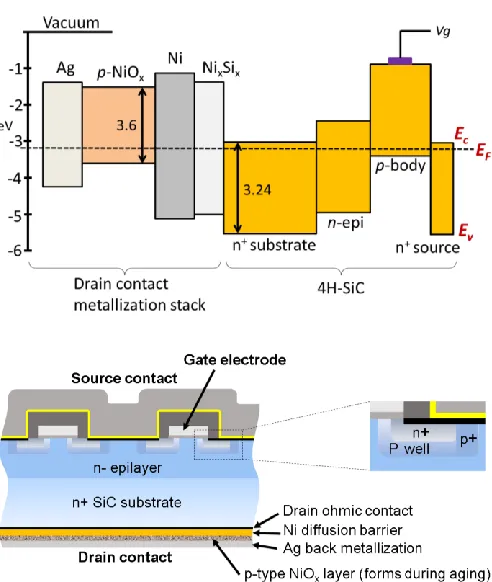
This non-linear or rectifying type output characteristic has been demonstrated before for nickel silicide based 4H-SiC ohmic contacts aged in air for 150 h at 400 °C [6]. In that case, the author attributed this to degradation of the ohmic contact itself. However, we present an alternative theory here, based around the formation of the NiOx layer presented earlier: this rectifying behavior seems to be equivalent to that of a diode in series with the drain-source current. It also emulates the output characteristics of a Si IGBT, which has the same basic structure as a DMOSFET but uses a p+ substrate. Our diode theory then appears to be plausible, since the nickel oxide is a well-known p-type semiconductor. The device cross section and associated band diagram is shown in Fig. 13. It can be seen from this that the material layers in between the p-type NiOx and n-type SiC substrate layers are metals, or metal-like, and therefore act like highly doped n-type semiconductors. We therefore propose that the SiC MOSFET devices effectively have a heterojunction diode in series with their drain contacts and this causes the non-linear output characteristic after a period of aging in an oxygen containing atmosphere.
2) Additional time delayed VDS0 on-state losses
This IGBT like rectifying response will impose an additional conduction loss in the same way as for an IGBT’s VCE0 built-in potential parameter, in addition to the normal temperature dependent MOSFET on-state losses. Eqn. 1 shows the total conduction losses for this new situation, where VDS0 is the built-in potential value of VDS at the knee in the non-linear curves shown for these SiC MOSFETs in Figs. 10 and 11, and is equivalent to the IGBT’s VCE0 parameter. As can be seen from this equation, the I2.R
DS,ON losses occur for the entire operation from time T0 to T2. However, the new losses due to the built-in potential only occur from time T1, after the output characteristics become non-linear.
(1)
3) Feasibility of operating in air or low oxygen environments
results in increased on-state losses, and not outright failure, the good performance of these SiC MOSFET devices at very high temperatures opens up the possibility of operating the devices in air. Low vacuum or inert gas sealed atmospheres with inherently low but non-zero oxygen levels might also be considered as alternatives to hermetic sealing or high temperature capable silicone gels or other alternative encapsulates. However, when operating in such atmospheres, care must be taken to ensure that high leakage or breakdown at the edges of the device occurs at the working temperature of choice, and under real switching transients with real loads. When tested in air for reverse breakdown, we have seen arcing at the edges of some SiC MOSFET types at less than their rated breakdown voltages, while this was not found for other types even slightly above their breakdown voltages. This presumably is because some manufacturers have designed their device terminations to reduce the electric field close to the edge of the die more than others, and-or have used different passivation materials with different insulation strengths.
4) Influence of die attach on aging
We have attributed the sudden appearance of the non-linear response to correlate with the occurrence of a continuous layer of nickel oxide (previously shorted out) after long periods of oxygen exposure at high temperature. In these tests, the die were simply placed drain-side down on a hotplate, and were not bonded to the surface. In real applications, the die will be bonded to a substrate with a die attach material. We therefore expect the diffusion of oxygen to be delayed by the die attach
material and to occur first at the outer edges of the die. In a porous die attach microstructure, such as silver sintered bonds, there may be fast paths for oxygen diffusion, particularly if the microstructure has coarsened due to either high temperature cycling stresses [25] or high temperature storage stresses [26]. As mentioned in the introduction to this paper, much work has been done by other authors to evaluate oxygen barriers between the ohmic contact(s) and the final metallization layer, whether it be aluminum on the source contact side for wire bonding or silver on the drain side for soldering. However, it is not known currently whether the devices being evaluated in the present work have been fabricated with such features. In either case, our results suggest that these devices would benefit from the implementation of a higher performance oxygen barrier to enable them to survive for longer in an oxygen containing environment than we have demonstrated in this work.
5) Lifetime of die compared to packaging
It is possible that the device packaging may fail in other ways before this degraded output characteristic occurs for the devices, particularly in thermal cycled applications where the thermo-mechanical stresses can be extremely high. For example, earlier in this work, we reported that the SiC MOSFET die survived 1000 temperature cycles from 0 °C to 350 °C. However, in our previous works, we have demonstrated much shorter lifetimes under the same temperature cycling conditions for various candidate high temperature capable die attach materials and DCB-type substrates [27, 28]. In the future, as the requirement for a high temperature operating capability becomes more widespread, and the SiC power devices are made available at higher temperature ratings, it is highly likely that the packaging materials will be improved accordingly.
V. SUMMARY AND OUTLOOK
We have demonstrated the feasibility of operating these commercially-available second generation SiC DMOSFET devices at temperatures well above their rated temperatures, even as high as 350 °C. The devices showed excellent forward and reverse characteristics up to this temperature. However, the RDS on-state losses are extremely high at high temperatures and, when added to switching losses, will have to be managed by current de-rating, dimensioning the cooling system, and-or limiting the periods of high temperature operation. The threshold voltages are also unstable at high temperatures and drift significantly from their nominal values. Some amount of drift is likely to feature in the next generations of devices, at least at very high temperatures and gate potentials. For the devices under test in this work, the positive drift appears to cause only minor current reductions and can be compensated for in the system design. There appears to be a risk that the significant negative drift demonstrated in this work could potentially allow the threshold voltage to reduce as far as the gate turn-off bias, and cause some devices to enter a normally-on state at very high operating temperatures. Recommendations were made to mitigate this risk. Exposure to oxygen at high temperatures has been shown to eventually cause a sudden increase in on-state losses due to the
Fig. 13. Band energy alignment diagram and associated simplified SiC D-MOSFET device structure, indicating the position of the NiOx layer that
[image:12.612.49.295.43.334.2]degradation of the drain contact metallization. The additional heat generated will then place an addition burden on the cooling system and power module packaging. When practical, these additional losses can be accounted for in the system design.
REFERENCES
[1] J. Richmond, L. Cheng, A. Agarwal, and J. Palmour, "Characterization of a Large Area Silicon Carbide PiN Diode at Temperatures up to 900°C," Additional Conferences (Device
Packaging, HiTEC, HiTEN, & CICMT), vol. 2012, pp.
000384-000387, 2012.
[2] P. G. Neudeck, R. S. Okojie, and L.-Y. Chen, "High-temperature electronics - a role for wide bandgap semiconductors?,"
Proceedings of the IEEE, vol. 90, pp. 1065-1076, 2002.
[3] R. S. Keen, L. R. Loewenstern, and G. L. Schnable, "Mechanisms of Contact Failure in Semiconductor Devices," presented at Reliability Physics Symposium, 1967. Sixth Annual, 1967. [4] H. J. Fecht, J. W. Mrosk, and M. Werner, "Electrical contacts and
degradation mechanisms," presented at High Temperature Electronics, 1999. HITEN 99. The Third European Conference on, 1999.
[5] K. Gottfried, J. Kriz, J. Leibelt, C. Kaufmann, and T. Gessner, "High temperature stable metallization schemes for SiC-technology operating in air," presented at High-Temperature Electronic Materials, Devices and Sensors Conference, 1998, 1998.
[6] A. V. Kuchuk, M. Guziewicz, R. Ratajczak, M. Wzorek, V. P. Kladko, and A. Piotrowska, "Thermal degradation of Au/Ni2Si/n-SiC ohmic contacts under different conditions," Materials Science
and Engineering B-Advanced Functional Solid-State Materials,
vol. 165, pp. 38-41, 2009.
[7] R. S. Okojie, D. Lukco, Y. L. Chen, and D. J. Spry, "Reliability assessment of Ti/TaSi2/Pt ohmic contacts on SiC after 1000 h at 600 °C," Journal of Applied Physics, vol. 91, pp. 6553-6559, 2002.
[8] D. J. Spry and D. Lukco, "A Bondable Metallization Stack That Prevents Diffusion of Oxygen and Gold into Monolithically Integrated Circuits Operating Above 500°C," Journal of
Electronic Materials, vol. 41, pp. 915-920, 2011.
[9] M. Vincent, Z. Junqin, C. Carraro, and R. Maboudian, "A SiC metallization scheme using an ALD protective layer for harsh environment devices," presented at Micro Electro Mechanical Systems (MEMS), 2012 IEEE 25th International Conference on, 2012.
[10] A. Virshup, F. Liu, D. Lukco, K. Buchholt, A. Spetz, and L. Porter, "Improved Thermal Stability Observed in Ni-Based Ohmic Contacts to n-Type SiC for High-Temperature Applications,"
Journal of Electronic Materials, vol. 40, pp. 400-405, 2011.
[11] P. G. Neudeck, D. J. Spry, L. Y. Chen, G. M. Beheim, R. S. Okojie, C. W. Chang, R. D. Meredith, T. L. Ferrier, L. J. Evans, M. J. Krasowski, and N. F. Prokop, "Stable Electrical Operation of 6H SiC JFETs and ICs for Thousands of Hours at 500°C," IEEE
Electron Device Letters, vol. 29, pp. 456-459, 2008.
[12] S. Sundaresan, R. Singh, and R. W. Johnson, "SILICON CARBIDE “SUPER” JUNCTION TRANSISTORS OPERATING AT 500 °C," Additional Conferences (Device Packaging, HiTEC,
HiTEN, & CICMT), vol. 2012, pp. 000162-000166, 2012.
[13] B. G. S. Sundaresan, D. Hamilton, R. Singh, "Improvement of the Current Gain Stability of SiC Junction Transistors," Materials
Science Forum, Trans Tech Publications, Switzerland, vol.
Volumes 821-823, pp. 822-825, 2014.
[14] L. Cheng, A. K. Agarwal, S. Dhar, S.-H. Ryu, and J. W. Palmour, "Static Performance of 20 A, 1200 V 4H-SiC Power MOSFETs at Temperatures of −187°C to 300°C," Journal of Electronic
Materials, vol. 41, pp. 910-914, 2012.
[15] S. H. Ryu, S. Krishnaswami, B. A. Hull, B. Heath, F. Husna, J. Richmond, A. Agarwal, J. Palmour, and J. Scofield, "A comparison of high temperature performance of SiC DMOSFETs and JFETs," in Silicon Carbide and Related Materials 2006, vol.
556-557, Materials Science Forum, N. Wright, C. M. Johnson, K. Vassilevski, I. Nikitina, and A. Horsfall, Eds. Stafa-Zurich: Trans Tech Publications Ltd, 2007, pp. 775-778.
[16] R. Kaplar, S. DasGupta, M. Marinella, B. Sheffield, R. Brock, M. Smith, and S. Atcitty, "Degradation mechanisms and characterization techniques in silicon carbide MOSFETs at high temperature operation," Proc. Electrical Energy Storage
Applications and Technologies, pp. 121-124, 2012.
[17] R. J. Kaplar, D. R. Hughart, S. Atcitty, J. D. Flicker, S. DasGupta, and M. J. Marinella, "Performance and Reliability Characterization of 1200 V Silicon Carbide Power MOSFETs at High Temperatures," Additional Conferences (Device Packaging,
HiTEC, HiTEN, & CICMT), vol. 2013, pp. 000275-000280, 2013.
[18] M. Gurfinkel, J. Suehle, J. B. Bernstein, Y. Shapira, A. J. Lelis, D. Habersat, N. Goldsman, and Ieee, Ultra-fast characterization of
transient gate oxide trapping in SiC MOSFETs. New York: Ieee,
2007.
[19] K. Matocha, "Challenges in SiC power MOSFET design,"
Solid-State Electronics, vol. 52, pp. 1631-1635, 2008.
[20] S. Tanimoto and H. Ohashi, "Reliability issues of SiC power MOSFETs toward high junction temperature operation," physica status solidi (a), vol. 206, pp. 2417-2430, 2009.
[21] D. A. Gajewski, S. H. Ryu, M. Das, B. Hull, J. Young, and J. W. Palmour, "Reliability Performance of 1200 V and 1700 V 4H-SiC DMOSFETs for Next Generation Power Conversion Applications," Materials Science Forum, Silicon Carbide and
Related Materials 2013, vol. 778-780, pp. 967-970, 2014.
[22] A. J. Lelis, D. Habersat, R. Green, A. Ogunniyi, M. Gurfinkel, J. Suehle, and N. Goldsman, "Time dependence of bias-stress-induced SiC MOSFET threshold-voltage instability measurements," Ieee Transactions on Electron Devices, vol. 55, pp. 1835-1840, 2008.
[23] C.-T. Yen, C.-C. Hung, H.-T. Hung, C.-Y. Lee, L.-S. Lee, Y.-F. Huang, and F.-J. Hsu, "Negative bias temperature instability of SiC MOSFET induced by interface trap assisted hole trapping,"
Applied Physics Letters, vol. 108, pp. 012106, 2016.
[24] A. T. Bryant, N. A. Parker-Allotey, I. R. Swan, D. P. Hamilton, P. A. Mawby, T. Ueta, T. Nisijima, and K. Hamada, "Validation of a fast loss and temperature simulation method for power converters," presented at Integrated Power Electronics Systems (CIPS), 2010 6th International Conference on, 2010.
[25] D. P. Hamilton, M. R. Jennings, Y. K. Sharma, C. A. Fisher, O. Alatise, and P. A. Mawby, "Evaluation of commercially available SiC devices and packaging materials for operation up to 350°C," in ECCE. Pittsburgh, USA: IEEE, 2014.
[26] H. Zhang, S. Nagao, K. Suganuma, H. J. Albrecht, and K. Wilke, "Reliability Improvement of high Temperature sintered Ag Die-Attachment by adding Sub-micron SiC Particles," presented at PCIM Europe 2015; International Exhibition and Conference for Power Electronics, Intelligent Motion, Renewable Energy and Energy Management; Proceedings of, 2015.
[27] D. P. Hamilton, A. Syed-Khaja, J. Franke, and P. A. Mawby, "High temperature thermal cycling reliability of silver sintered and electroplated tin based transient liquid phase joints," presented at Integrated Power Systems (CIPS), 2016 9th International Conference on, Nuremberg, Germany, 2016.
[28] D. P. Hamilton, S. Riches, M. Meisser, L. Mills, and P. A. Mawby, "High temperature thermal cycling performance of DBA, AMB and thick film power module substrates," presented at Integrated Power Systems (CIPS), 2016 9th International Conference on, Nuremberg, Germany, 2016.
Dean P. Hamilton received his first degree and
worked as a Research Fellow in the School of Engineering Power Electronics Research Group. He has worked as part of a team to develop and validate a fast inverter simulator for Toyota, Japan, to model the continuous power cycling of IGBTs, and then on a low carbon vehicle project to evaluate SiC MOSFETs and packaging. His current project and research interests are on the high temperature reliability and performance of SiC power devices and packaging materials for future high temperature capable power modules and converters. He is a member of the Materials Research Society and a frequent reviewer of IEEE journal publications.
Michael R. Jennings was born in Neath, Wales, in
1980. He received the B.Eng. degree in Electronics with Communications from the University of Wales, Swansea, U.K., in 2003. The B.Eng. degree incorporated a second year (exchange program) of study in the USA, where he studied at Union College, Schenectady, NY, USA. He then undertook the Ph.D. degree in power semiconductors from the University of Warwick, Coventry, U.K. During the Ph.D. degree, he has won travel scholarships from the IEE (Hudswell Bequest Fellowship) and Welsh Livery Guild for electrical engineering research purposes. The scholarships obtained allowed him to visit Rensselaer Polytechnic Institute, Troy, NY, USA, in 2005. In 2009, he was awarded a Science City Research Alliance Fellowship, sponsored by the European Regional Development Fund and Advantage West Midlands. The focus of his research within this remit was the development of Silicon carbide devices. His current research topics include high voltage bipolar devices (PiN diodes and Thyristors) in SiC, novel gate oxidation processes for FETs and 3C-SiC (cubic) growth above direct wafer bonded Si/SiC structures. He is also a Lecturer on the first year general engineering electronics course.
Amador Pérez-Tomás. From 1999 to 2001 he
worked in the private sector for Hewlett-Packard. PhD in Physics in 2005 (UAB). Research fellow at the University of Warwick, England (2006-2008). CSIC RyC 2008-2014. In 2014 he joined the ICN2. Current research activities are engineering wide bandgap semiconductors and perovskite materials for novel electronic and optoelectronic devices. He has authored or coauthored more than 150 journal papers and conferences on the topic. He is founder of SME Wismok SL (Orbital 40, SME Seal of Excellence).
Stephen A. O. Russell was born in Kent, England in
1984. He received an MSci (Hons) degree in Physics from the University of Birmingham in 2007, an MSc in Nanotechnology from University College London in 2009 and a PhD in Electronic Engineering from the University of Glasgow in 2013. Between 2013 and 2014 he was a Postdoctoral Research Assistant at the University of Glasgow continuing with research in to diamond electronics particularly FETs for high performance applications and has authored several papers on this topic. In 2014 he was appointed a Research Fellow at the University of Warwick to work on high voltage blocking (10 kV) silicon carbide MOSFETs.
Steven A. Hindmarsh joined the University of
Warwick in 2011 as a Trainee Technician. He has since progressed to the position of Senior Research Technician working within the newly created Warwick Microscopy Research Technology Platform. Within this central facility he is involved in a diverse range of projects with researchers from both academia and industry. His main interest is in FIB-SEM, preparing samples from challenging materials and conducting SEM and TEM based investigations.
Craig A. Fisher was born in Warwickshire, U.K., in
1984. He received the M.Sc. degree in Advanced Electronics Engineering, and the Ph.D degree in the field of silicon carbide power electronics from the University of Warwick, Coventry, U.K., in 2010 and 2014, respectively. This Ph.D degree focused on three principle areas: novel edge termination solutions for high voltage power devices, carrier lifetime enhancement using high temperature processes, and the formation of robust ohmic contacts to p-type 4H-SiC. He then spent 12 months as a Research Fellow with the School of Engineering, University of Warwick, where his research interests included the design, fabrication and characterization of 4H-SiC MOSFETs and diodes for high voltage (>3.3 kV) applications. Since January 2015, he was worked in the semiconductor industry, developing silicon carbide power devices. He has authored (or co-authored) over 30 journal / international conference papers, and has acted as a reviewer for the IEEE Transactions on Semiconductor Manufacturing and for the IET."
Philip A. Mawby (S'85-M'86-SM'01) received the