University of Warwick institutional repository: http://go.warwick.ac.uk/wrap
A Thesis Submitted for the Degree of PhD at the University of Warwick
http://go.warwick.ac.uk/wrap/62963
This thesis is made available online and is protected by original copyright. Please scroll down to view the document itself.
The Development of Model Organic Decoupling
Films for use on Strongly-Interacting Metal
Surfaces
Thomas William White
A thesis submitted in partial fulfilment
of the requirements for the degree of
Doctor of Philosophy in Chemistry
Department of Chemistry
University of Warwick
1
Contents
Contents ... 1
List of tables and figures ... 5
Declaration ... 19
Acknowledgements ... 20
Abstract ... 21
Abbreviations ... 23
Chapter 1 ... 24
1.1 Surface engineering ... 24
1.2 The role of the substrate ... 28
1.2.1 Adsorbate and substrate structural modifications ... 29
1.2.2 Electronic interactions between molecule and substrate ... 30
1.3 Characterising sample surfaces ... 32
1.4 Controlling the molecule-substrate interaction ... 34
1.4.1 The ‘Lander’ approach to decoupling ... 37
1.4.2 Ultra-thin decoupling layers... 38
1.4.2.1 Alkali halide decoupling films ... 39
2
1.4.3 Organic decoupling layers ... 43
1.4.3.1 Alkanethiol decoupling films ... 45
1.5 Carboxylic acids on copper surfaces ... 46
1.5.1 Benzyl acids on copper surfaces ... 47
1.5.2 Non-benzyl acids on copper ... 50
1.6 Structure of thesis ... 54
1.7 Chapter 1 references ... 55
Chapter 2 ... 63
2.1 Scanning tunnelling microscopy ... 65
2.1.1 Background ... 65
2.1.2 Measurement methodology ... 69
2.2 Low-energy electron diffraction ... 71
2.3 X-ray photoemission spectroscopy ... 74
2.4 Near-edge X-ray adsorption fine structure spectroscopy ... 77
2.5 Theoretical methods ... 80
2.5.1 Methods - molecular mechanics ... 82
2.5.2 Methods - density functional theory ... 83
2.6 Fabrication of molecule-on-metal films ... 85
2.6.1 UHV system ... 85
2.6.2 Sample cleaning ... 87
2.6.3 Adsorbate deposition ... 88
2.7 Chapter 2 references ... 90
Chapter 3 ... 92
3.1 TPA on Cu(110) ... 97
3
3.1.2 The (14×2) structure ... 103
3.1.3 (The 6×2) structure ... 104
3.1.4 Intact TPA on Cu(110) ... 106
3.1.5 Phase transitions of TPA on Cu(110) ... 108
3.1.6 TPA on Cu(110) - summary... 110
3.2 TPA on Cu(111) ... 110
3.2.1 TPA H-bonded phase... 110
3.2.1.1 Theoretical investigation of TPA on Cu(111) ... 115
3.2.2 Effect of annealing on the TPA brickwork film ... 125
3.2.2.1 TP on Cu(111) – terrace-bound structures ... 126
3.2.2.1 TP on Cu(111) – step-bound structures ... 128
3.2.3 Fe-TP structures ... 130
3.2.3.1 Deposition of Fe onto the TPA brickwork-like film ... 132
3.3 Summary of TPA on Cu surfaces ... 136
3.4 Chapter 3 references ... 138
Chapter 4 ... 142
4.1 OA on Cu(110) ... 143
4.1.1 Local-scale structural features of OA on Cu(110) ... 147
4.1.2 DFT of OA on Cu(110) ... 151
4.1.3 Photoelectron spectroscopy of OA on Cu(110) ... 155
4.1.4 Summary of OA on Cu(110) ... 159
4.2 OA on Cu(111) ... 161
4.2.1 Flat-lying OA phase on Cu(111) ... 161
4.2.2 Vertically-standing OA phase on Cu(111) ... 165
4.2.2.1 Local-scale structural features in the OA film... 168
4
4.4 Chapter 4 references ... 172
Chapter 5 ... 174
5.1 TPA on the OA (3×2) monolayer ... 175
5.1.1 TPA adsorption geometry: on top of the OA? ... 177
5.1.2 Deposition of TPA onto a OA film held at LT ... 182
5.2 TPA on the OA film ... 183
5.2.1 TPA adsorption geometry ... 186
5.2.2. Assembly of the ‘on-top’ TPA structures ... 189
5.3 Summary of TPA on OA decoupling films ... 192
5.4 Chapter 5 references ... 194
Chapter 6 ... 196
6.1 TPA on Cu(110) and Cu(111) ... 197
6.2 OA on Cu(110) and Cu(111) ... 199
6.3 TPA overlayers on the OA monolayer films ... 200
5
List of tables and
figures
Chapter 1: Introduction
Figure 1.1 Schematic representation of the top-down and bottom-up approaches to the fabrication of nanostructures on surfaces. In the top-down approach, structure is imposed on a material ‘from above’ using classical techniques that add or remove material. In the bottom-up approach, the inherent interactions between smaller components are harnessed such that they assemble into the required structure
Figure 1.2 Schematic representation of the electronic structure of a molecule (red dumbbell shape) in the gas-phase (left) and adsorbed on a metal surface (right). In the gas phase, the electronic structure is energetically well-defined. In contrast, when adsorbed on the metal, the hybridisation of the molecular and metallic electronic states results in their energetic and spatial distributions being broadened.
Figure 1.3 a) Schematic representation of the adsorbate charge screening on metal surfaces. b) The HOMO-LUMO gap, labelled Eg, as a function of the
molecule-substrate separation.
6
Figure 1.5 a Concept model for the ‘molecular Lander’. Adapted from reference [62]. b) and c) Side on views of an example Lander molecule in the gas-phase and adsorbed on a metal surface, respectively. Adapted from reference [30].
Figure 1.6 a) Schematic representation of the decoupling layer strategy. A thin layer of an insulating material is deposited onto the surface prior to adsorption of the molecular tecton. b The ‘multilayer approach’ to decoupling, where a thick film of the organic species is deposited. The lower layers act as a decoupling layer.
Figure 1.7 a) Side-view schematic of a NaCl bilayer decoupling film. The substrate is shown in grey, the Na ions are blue, the Cl in green, and the decoupled molecules are shown as red dumbbells. b Depiction of the ‘carpet’ growth of NaCl over Ge(001), adapted from reference [69]. The substrate atoms are shown with partially shaded circles, the fully shaded circles show the Cl- ions within the NaCl structure.
Figure 1.8 a) and b) STM images of Pd atoms adsorbed on the NiAl(110) surface oxide film. The corresponding STS spectra of Pd atoms in each position are shown in c). Adapted from reference [68].
Figure 1.9 Three component model demonstrating the versatility of organic decoupling layers. The head and tail groups control the interaction between the decoupling layers and the substrate and overlayer adsorbates respectively. The backbone controls the thickness and the rigidity of the organic layer.
Figure 1.10 Schematics of the various ways in which alkanethiol films have been utilised as decoupling layers. In a), the functional species is deposited directly onto the alkanethiol film, whilst in b) the alkanethiol tail group is selected to specifically control the adsorption of the overlayer species. c) shows how a functional species can be functionalised with an alkanethiol chain prior to deposition on the metal surface.
7
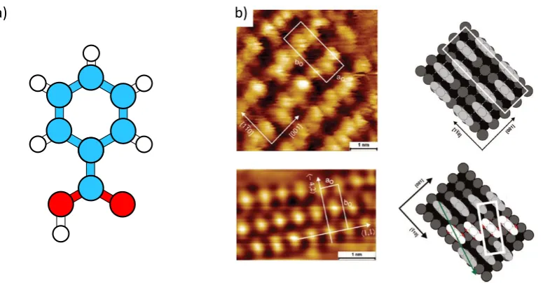
Figure 1.12 a) Schematic of benzoic acid. The blue, white and red represent carbon, hydrogen and oxygen respectively. b) STM images (left) and corresponding structures (right) of the benzoate structures on unreconstructed (top) and reconstructed (bottom) Cu(110) surfaces. Adapted from reference [108].
Figure 1.13 a) Schematic of formic acid (top) and acetic acid (bottom). b) STM image of the (2×2) formate structure on the Cu(110) surface. Adapted from reference [120]. c) STM image of the c(2×2) formate structure formed on the O-precovered Cu(110) surface. Adapted from reference [104]. d) STM image of the acetic acid chains obtained on the Cu(110) surface. Adapted from reference [130].
Figure 1.14 a) Schematic of oxalic acid. b) The tilting and bidentate adsorption geometries of oxalic acid identified on the Cu(110) surface. Adapted from reference [103]. c) STM image of the flat-lying oxalate structure reported on Cu(111). Adapted from reference [127].
Chapter 2: Experimental and theoretical methods
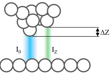
Figure 2.1 Schematic of the STM experiment. The tip is moved over the sample by the piezoactuators (orange box), whilst a voltage is applied between the tip and sample. The tunnel junction is depicted in the red circle.
Figure 2.2 Schematic of the tunnel junction, revealing the derivation of the different terms comprising Equation 2.5 and how the tunnel current decreases with increased tip-sample separation.
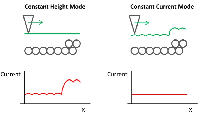
Figure 2.3 Depiction of the tip trajectory as it is scanned in constant height and constant current modes. The green line shows the position of the tip as it is scanned over the sample. In the bottom profiles, the measured current is displayed as a function of position, assuming a perfect feedback system.
8 array of spots, the colour of which depends on their energy and direction. The blue electrons show the primary electron beam being fired at the sample, the red and green are the inelastically and elastically back-scattered electrons, respectively. b) Example LEED pattern of a clean Cu(110) surface.
Figure 2.5 a) Model demonstrating how the real space structure of a surface is depicted in reciprocal space in the LEED pattern. b) Demonstration of how a superstructure is shown in the LEED as a consequence of the reciprocal depiction. The red squares indicate the adsorbate positions (top image) and the additional spots they generate in the LEED pattern (lower image).
Figure 2.6 Mean free path of electrons as they travel through an inorganic lattice. Adapted from reference [13]. The black dots correspond to data points obtained from a variety of different materials.
Figure 2.7 a) Schematic of the XPS process. b) The photoemission process in terms of the electron energy levels.
Figure 2.8 Schematic depiction of a XPS spectrum, whereby the obtained spectrum is shown in red, the fitted peak in green, and the background in blue.
Figure 2.9 a) Schematic of the Auger emission process. b) Energy level depiction of the transitions involved in NEXAFS.
Figure 2.10 a) Schematic of TPA molecule (upper) and side view (lower). In the side view, the σ- and π-orbitals are shown by the green and orange dumbbell shapes, respectively. b) NEXAFS spectra taken of TPA on rutile TiO2(110) at low molecular
coverage. c) NEXAFS spectra taken of TPA on rutile TiO2(110) at 1 monolayer
coverage. The angles in b) and c) are the photon incidence angle with respect to the surface, as depicted by the inset of b). The σ- and π-signals are colour-coded using green and orange bands, respectively. Both b) and c) are adapted from reference [18].
9
Figure 2.12 a) Photograph of the LT-UHV-STM used in many of the experimental
studies presented here. The three chambers have been highlighted with different colours; the loadlock in blue, the preparation chamber in green and the STM chamber in red.
Figure 2.13 a) Schematic of the evaporation of low vapour pressure molecules. b) Photo of the loaded OA doser, as mounted on chamber. c) Schematic of the OA doser. The blue boxes represent CF flanges. The two valves are labelled (1) and (2). LL represents the loadlock.
Chapter 3: Terephthalic acid on Cu(110) and Cu(111)
Table 3.1 Summary of the dimeric H-bond lengths reported for TPA on a number of different weakly-interacting surfaces and in bulk TPA crystals. The * indicates a H-bond length that has been corrected to use a TPA molecular length of ~7Å.
Figure 3.1. a) and b) plan views of the (110) and (111) surfaces. c) Molecular structure of TPA. d) STM image (adapted from reference [5]) and schematic of the TPA brickwork superstructure.
Figure 3.2 Examples of TP MO structures. a) STM images and structural models of the porous Fe-TP films obtained on Cu(001), adapted from reference [17]. b) STM image and structural model of the chiral Fe-TP ‘flowers’ fabricated on the Cu(11 surface, adapted from reference [16].
Figure 3.3 a) STM images and structural models of the TPA 1D chains and TP brickwork-like structure obtained on the Pd(111) surface. Adapted from reference [10]. b) STM images and corresponding models of the three temperature-dependent TPA phases observed on Cu(001). Adapted from reference [11].
10
Figure 3.5 a) LEED pattern of the (10×2) TPA network on Cu(110). Two of the crystallographic spots are labelled. E=60 eV. b) c(5×2) LEED pattern as simulated by the LEEDpat3.0 software [28].
Figure 3.6 a) and b) C 1s and O 1s XPS spectra of the (10×2) TPA layer. The C 1s shows peaks at 284 eV and 288 eV, representing the aromatic and carboxylate carbons, respectively. The O 1s shows only a single, narrow peak, centred at 531 eV, arising from the chemically-identical O atoms in the carboxylate moiety.
Figure 3.7 a) and b) Structural model and simulated STM image of the lowest energy (10x2) TPA structure, as calculated by DFT. The simulated image was obtained using the DOS between the Fermi energy and a bias potential of 0.5 eV.
Figure 3.8 a), b) and c) STM image (I=800 pA, U=-1.2 V), model and simulated STM image of the (14×2) structure on Cu(110), respectively. The blue arrow in (a) shows the position of the Cu adatoms, imaged as a darker line.
Figure 3.9 a) and b) STM image and LEED pattern of the (6×2) TP phase on Cu(110). a) I=800 pA, U=-1.2 V. b) E=61 eV. c) and d) DFT-calculated lowest energy structure and simulated STM image of the (6×2) film.
Figure 3.10 a) and b) C 1s and O 1s XPS spectra, respectively, of the TPA multilayer film, measured at 190K. In the O 1s spectrum, the carboxylic peaks have been coloured red, the carboxylate green and the contaminant peak green.
11
Figure 3.12 STM images of the TPA H-bonded network on the Cu(111) surface, after deposition onto a RT substrate. The blue arrow indicates the straight edge of the molecular island. a) I=50 pA, U=1.3 V. b) shows a zoomed-in image of the islands internal structure. The green oval highlights a single TPA molecule and the blue circle demonstrates a defect in the organic lattice. I=100 pA, U=-1.0 V.
Figure 3.13 Two STM images showing a) weakly-correlated or randomly-arranged,
and b) strongly-correlated distribution of defects in the TPA lattice. The two images have been obtained from different sample preparations. The purple box indicates a short chain of defects. a) I=210 pA, U=1.4 V. b) I=33pA, U=-0.9V.
Figure 3.14 MM study of the TPA-TPA interactions. a) shows a schematic of the unit cell used in the MM calculations, revealing how the unit cell of the calculation was constructed to test the in-chain and inter-chain interactions. Vectors a and b
define the size and shape of the unit cell which, for the case of a single TPA row, is shown by the red dashed lines. b) Potential energy profile calculated as a function of
a. c) Potential energy surface as a function of bx and by for a fixed value of a.
Figure 3.15 a) Model of the initial TPA arrangement on Cu(111) used in the DFT calculations. The green rectangle shows the space explored by the DFT calculations, corresponding to the DFT-calculated potential energy surface shown in (b).
Figure 3.16 a) Derivation of the and parameters and the definition of the
and terms used to simulate the different interactions. b) Flow diagram showing how the proposed analytical model can be used to predict the effects of the interaction interplay. c) Illustration of the two chains of points used to depict the substrate and molecules in the algorithm. The blue dots indicate the positions of molecules, the red of the substrate.
12
Figure 3.18 Calculated distribution of TPA molecules from the model described in the text. The red circles represent the positions of substrate lattice sites. The blue circles show the positions of the TPA molecules and define the lower boxes showing the intermolecular separations. These are reported in units of lattice parameters (top) and actual distances (bottom). The colour coding shows where the bonds are shorter (green) or longer (blue) than the separation predicted from the intermolecular interaction alone.
Figure 3.19 STM images of the TP structures fabricated by annealing the H-bonded TPA phase to 353K. a) shows an overview of the features found, including the terrace-bound structures and the 2D stripes observed at steps. I=70pA, U=1.6 V. b) Zoomed in view of the terrace-bound structures, demonstrating the variety of motifs observed. I=40pA, U=-1.4 V.
Figure 3.20 a) STM image of two TP monomers. The blue line illustrates the position of the line profile shown in c). A TP model has been overlaid on the upper feature. I=40pA, U=-1.4 V. b) 3D representation of the image in a) to highlight the depressions at the ends of the TP molecules.
Figure 3.21 a) STM image of two TP trimers. The trimer on the right is overlaid with a structural model including a single Cu adatom. I=50 pA, U=-1.9 V. b) STM image of a TP tetramer and, inset, the same image with an overlay of a tentative model with two Cu adatoms. I=30 pA, U=-1.9 V.
Figure 3.22 a) Large-range STM image, showing 1D stripes (highlighted by blue boxes) and 2D islands (highlighted by green boxes). I=100 pA, U=-1.0 V. b) Zoomed in image of a 2D island; the profile along the blue line is shown in c). d) Zoomed in STM image, overlaid with TP models. c) and d) I=110 pA, U=-1.0 V.
13 within the island, suggesting a (111)-like arrangement of the protrusions. The green arrows in b) shows the locations of steps within the island. I=1.3 nA, U=45 mV.
Figure 3.23 a) Large-range STM image of Fe islands grown on the Cu(111) surface held at 248 K during deposition. I=100 pA, U=1.0 V. The green circles highlight multilayer-high Fe islands. b) and c) Zoomed in topography and current images of a single Fe island, respectively. The current image is shown to highlight the resolution within the island, suggesting a (111)-like arrangement of the protrusions. The green arrows in b) shows the locations of steps within the island. I=1.3 nA, U=45 mV.
Figure 3.24 a) Large-range STM image of Fe deposited onto H-bonded TPA/ Cu(111) held at 248 K. I=40 pA, U=1.4 V. b) Zoomed in STM image of a TPA island after Fe deposition. Some protrusions consist of Fe adsorbed either on top or penetrating into the TPA lattice (blue circle), others correspond to single TPA molecules with enhanced contrast (green circle). I=40 pA, U=1.4 V.
Figure 3.25 a) Large-range and b) zoomed in STM images of the films in Figure 3.24 after annealing to 317 K. a) I=58 pA, U=-0.3 V. b). I=33 pA, U=0.4 V. The blue and green circles highlight trimer and tetramer motifs, respectively. The green line shows the line profile in c).
Figure 3.26 a) Large-range STM image of the films in Figure 3.24 after annealing to 383 K. I=33 pA, U=1.7 V. b) Zoomed-in STM image of the same sample, highlighting the apparent similarity to the MOCN-II structure shown in c) (figure taken from reference [15]). I=40 pA, U=-0.7 V. d) STM image of the same Fe-TPA structure after annealing to 403 K. I=58 pA, U=-0.5 V.
Chapter 4: Oxalic acid on Cu(110) and Cu(111)
14
Table 4.2 Total adsorption energies, as predicted by DFT, of mono-deprotonated OA adsorbed in an upright geometry on the Cu(110) surface, using different molecular packings.
Figure 4.1. a) STM image of the OA film on the Cu(110) surface prior to annealing. Small ordered regions can be found amidst non-resolvable areas. I=120 pA, U=-1.1 V. b) STM image of the OA film after annealing to 398 K, showing the long-range (3×2) ordering. The blue circle highlights an interstitial OA molecule and the green lines highlights a domain boundary between two (3×2) domains. I=180 pA, U=-1.1 V. c) STM image of the OA film after annealing to 423 K, demonstrating clean areas (blue circle), potential decomposition products (purple circle) and isolated OA features (green circle). I=100 pA, U=1.1 V. d) LEED image of the (3×2) OA film. E=148eV, T≈ T.
Figure 4.2 a LEED image of the ‘disordered ( 2 ’ OA phase. E=6 eV, T≈ T. b
Corresponding STM image. I=300 pA, U=-1.0 V.
Figure 4.3 Initially-assumed OA structure, viewed from above and along the [001] direction, based on the (3×2) structure found using STM and LEED and the upright orientation suggested in reference [1] from RAIRS studies.
Figure 4.4 a) Possible positions of the interstitial OA if it maintains the same adsorption site as the surrounding OA molecules. In either of the two positions, the molecule is no longer centred within the (3×2) cell. b) Alternative adsorption site compatible with the a symmetric c(3×2) configuration. c) and d) STM images of the OA (3×2) structure, imaged at positive and negative bias voltages, respectively. I=180 pA. e) Profiles of the two lines in a) and b), highlighting the apparent height differences in empty and filled state imaging.
15
Figure 4.6 a) and b) Sequential STM images of a domain boundary with a 3× periodicity along the [110] direction. The OA molecule highlighted with the blue arrow is seen to move one Cu lattice spacing to the left between the two scans. I=110 pA, U=1.2 V. c) Schematic representation of the diffusion barriers along the two principal crystallographic directions of the Cu(110) substrate.
Figure 4.7 a) and b) O 1s spectra of the OA monolayer and multilayer films, respectively. c) and d) C 1s spectra of the OA monolayer and multilayer films, respectively. The peak assignment is discussed in the text.
Figure 4.8 a) Top and side views of OA, showing the relative orientations of the σ- and π-states (orange and green, respectively). The NEXAFS spectra of the OA (3×2) monolayer, acquired with the photon incidence angle oriented along b) along the [001] direction and c) along the [110] direction. The photon polarisation vector of each scan are given with respect to the surface plane. In the two spectra, the σ- and π-transitions are highlighted by the green and orange bands, respectively.
Figure 4.9 Proposed adsorption geometry of the OA molecules, based on the results of the STM, LEED, DFT, XPS and NEXAFS measurements.
Figure 4.10 STM images showing the adsorption of OA on Cu(111) as a function of coverage. a-c) are adapted from reference [2], performed at 100 K. d-f) were obtained in this work. a) and d) show formation of formate. b) and e) The coexistence of the OA rhomboidal phase and formate. c) and f) Zoomed in STM images of the rhomboidal structure of the OA phase. d) I=100 pA, U=1.0 V. e) I=140 pA, U=-1.7 V. f) I=140 pA, U=-1.7 V. The crystallographic directions inset into d) only apply to d-f).
Figure 4.11 Model of the Cu-OA structure on Cu(111) as proposed by Faraggi et al. Image taken from reference [2].
16 in a) to 398 K. The green oval highlights a chain of second layer OA. I=57 pA, U=1.0 V.
Figure 4.13 a) Zoomed in STM image of the OA ( o monolayer phase on
the Cu(111) surface. I=190 pA, U=-1.4 V. b) and c) Two sequential STM images of the same area, highlighting removal of individual molecules by the tip in b) and deposition of OA molecules onto the OA monolayer in c). The contrast in b) and c) been selected so that the on-top OA molecules could be better resolved. b) and c) I=19 pA, U= -1.4 V.
Figure 4.14 LEED image of the OA ( o structure. E=105 eV, T=207 K.
Figure 4.15 Schematics of a potential a) flat-lying and b) vertically-standing OA monolayer on Cu(111 with a ( o
superstructure.
Figure 4.16 STM images of unidentified features obtained after OA monolayer preparation. a) Large area STM image I=140 pA, U=-1.4 V. b) and c) Sequential STM images of the porous OA structure, showing the dynamic nature of the structure. I=58 pA, U=-1.4 V.
Figure 4.17 Top-view models of a) the flat-lying OA film on the Cu(110) surface and b) the vertically-standing OA on the Cu(111) surface.
Chapter 5: Terephthalic acid on oxalic acid monolayers
Figure 5.1 a) STM image and model of the OA (3×2) monolayer film obtained on the Cu(110) surface. I=180 pA, U=-1.1 V. b) and c) STM images taken after TPA deposition onto the OA (3×2) film held at RT, showing the formation of [001]-oriented TPA stripes. The blue circle in c) indicates an unordered TPA structure. b) I=210 pA, U=-1.0 V. c) I=110 pA, U=-1.0 V.
17
Figure 5.3 STM image of TPA on the OA (3×2) film after annealing to 423 K. Gaps are now found in the OA lattice, whilst the TPA have maintained the same apparent brightness with respect to the OA molecules. I=65 pA, U=-0.9 V.
Figure 5.4 Schematic of the TPA molecules penetrating through the OA film to adsorb on the bare surface. The TPA initially adsorbs on top of the OA film (top). The OA is then displaced, so that the TPA can adsorb directly on the metal surface (bottom). The increased local OA density is a consequence of the TPA ‘squeezing’ the OA out of the way. The OA molecules and Cu(110) substrate supports have been faded in the top left panel, to clarify the TPA molecule.
Figure 5.5 a) Schematic of proposed TPA manipulation on-top of the OA film by the STM tip. b) Model demonstrating how the lack of TPA mobility fits a model where OA is displaced and TPA is directly adsorbed onto the copper substrate.
Figure 5.6 STM images of TPA on the OA (3×2) film, held at approximately 140 K during TPA deposition to limit OA mobility. a) Large range STM image. I=83 pA, U=1.4 V. b) Zoomed-in STM image of what is thought to be a single TPA molecule, circled, highlighting that there is no disruption to the OA lattice. I=58 pA, U=-1.8 V.
Figure 5.7 STM images and model of the ( O OA structure obtained on the Cu(111) surface. I=90 pA, U=-1.4 V. b-d) STM images acquired after TPA deposition onto the OA film held at RT. c) and d) show zoomed in images of the overlayer 2D islands and the 1D chains, respectively. b-c) I=14 pA, U=1.8V. d) I=100 pAm U=-0.9 V.
Figure 5.8 a-d) A series of sequentially-acquired STM images, showing overlayer 1D TPA chains on the OA/Cu(111) film. The chain highlighted in blue is disassembled by its interaction with the scanning tip, whilst that in green remains intact and can be used as a reference marker. The green arrows in b) and c) indicate the positions of the displaced TPA. All STM images taken at I=100 pA, U=-1.8 V.
18 line-by-line flattening is applied to this image due to tip-switching events. I=100 pA, U=1.8 V. b) Zoomed-in image of the TPA island after manipulation of the TPA molecules. I=40 pA, U=-1.8 V. c) Zoomed-in image showing the OA exposed after TPA manipulation. I=40 pA, U=-1.8 V.
Figure 5.10 a) STM image of TPA on the vertically-standing OA film on the Cu(111), demonstrating the perpendicular orientations of TPA 2D-islands and 1D-chains. Inset are the substrate crystallographic directions. I=14 pA, U=1.8 V. The directions of the 2D-islands (upper) and 1D-chains (lower) are also shown. b-c) Proposed models for the TPA chains and islands on the OA lattice, based on the observed orientation and periodicity of the TPA. OA is shown as blue circles, the TPA as the orange ovals.
Declaration
I hereby declare that this thesis, submitted in partial fulfilment for the degree of Doctor of Philosophy, represents my own work and has not been previously submitted to this or any other institution for another qualification. Work was carried out between October 2009 and July 2013 under the supervision of Dr Giovanni Costantini.
Both Chapters 3 and 4 contain contributions from collaborators, which are outlined in each section. Part of the work in Chapter 3 can be found in a published article, as outlined in the list of publications on Page 202. The room temperature scanning tunnelling microscope measurements of terephthalic acid on Cu(110) were performed by Dr Yeliang Wang and the corresponding density functional theory simulations by Dr Stefano Fabris. All of the theoretical simulations of terephthalic acid on Cu(111), including the molecular mechanics, density functional theory and the development of the analytical algorithm, have been performed by Dr Natalia Martsinovich and Professor Alessandro Troisi. The density functional theory calculations of oxalic acid on Cu(110) were performed by Dr Sara Fortuna and Dr Stefano Fabris.
20
Acknowledgements
There are many people I have to thank for their help and contributions to this work. Firstly, my eternal thanks go to my supervisor, Dr Giovanni Costantini. Thank you for the opportunity to work with you on this project. It has been a real pleasure and I know I have learned a lot.
I would also like to thank the many collaborators who I am honoured to have worked with; Dr Natalia Martsinovich, Professor Ale Troisi, Dr Yeliang Wang, Professor Klaus Kern, Dr Sara Fortuna, Dr Stefano Fabris, Dr Sam Haq, Dr David Duncan and Professor Phil Woodruff, to name just a few. I hope I am lucky enough to work with you again at some point in the future.
To my group and office mates, thank you for all your help and friendship. It was a blast, and I will miss you guys!
My heartfelt thanks also go to my family; I might stop boring you now with ‘molecules’. Probably not. Thank you for all the support and the love you have given me, particularly over the last few years. I am not sure I could have managed without you.
21
Abstract
Many of the highlights in the surface science field in the last years have arisen from the study of organic molecules adsorbed upon, but physically decoupled from, metallic substrates. When adsorbed on bare surfaces like Cu, the strong
interaction between the two can have a number of different effects on the chemistry, functionality and assembly of the adsorbates. These effects can be reduced or even
prevented by incorporating an ultra-thin insulating film between the molecule and the metal, enabling the retention of the desired molecular properties. Previous studies
have almost exclusively used films of inorganic material, such as alkali halides and metal oxides. In this work, an all-organic alternative approach has been developed, which should allow a greater degree of control over the nature of the decoupling film
and its corresponding interactions.
To demonstrate the potential impact of the molecule-substrate interaction on the formation of molecular nanostructures, the adsorption and assembly of a prototypical molecular tecton, terephthalic acid (TPA), has been explored on
Cu(110) and Cu(111). On Cu(110), the TPA is deprotonated and goes on to form a range of metal-organic or all-organic monolayer films. The exact structure obtained
22 characterised by both uncharacteristically short and elongated hydrogen bonds. This unusual assembly is the result of the oft-cited, but in general poorly understood, ‘interplay of intermolecular and molecule-substrate interactions’. In a bid to
understand the observed supramolecular assembly of TPA on Cu(111), a simple
algorithm has been developed that is capable of predicting both its quantitative and qualitative aspects. Moreover, this analytical model can be readily expanded to more complex assemblies, such as those using more complex molecules and surfaces. In
addition, the formation of Cu- and Fe-terephthalate complexes has been explored.
Oxalic acid (OA) monolayers have been investigated as prototype organic decoupling layers for the Cu(110) and Cu(111) surfaces. This molecule was chosen as, in previous work, it had been reported to adsorb in an upright orientation and
assemble into a densely packed monolayer on Cu(110). In this work, a flat-lying, low density film has been obtained on Cu(110), which later proved to be incapable
of supporting molecular ‘overlayers’ unless it was cooled to low temperature prior to the deposition of molecular overlayers. In contrast, a densely-packed, upright
monolayer was obtained on Cu(111). This decoupling layers was effective even at room temperature, and moreover appears to plays a significant role in determining the assembly of the overlayer species. These studies indicate the potential of
23
Abbreviations
1D, 2D, 3D 1-, 2-, 3-dimensional
bcc body-centred cubic
DOS Density of electronic states DFT Density functional theory
fcc face-centred cubic
H-bond Hydrogen bond
HOMO Highest occupied molecular orbital LEED Low-energy electron diffraction
LT Low temperature
LUMO Lowest unoccupied molecular orbital
MM Molecular mechanics
MO Metal-organic
NEXAFS Near-edge X-ray adsorption fine structure
OA Oxalic acid
PES Potential energy surface
RAIRS Reflection-adsorption infra-red spectroscopy
RT Room temperature
SAM Self-assembled monolayer STM Scanning tunnelling microscope STS Scanning tunnelling spectroscopy
TP Terephthalate
TPA Terephthalic acid
UHV Ultra-high vacuum
vdW van der Waals
24
Chapter 1
Introduction
1.1 Surface engineering
The engineering of surfaces with specific, predetermined properties is an important research goal. For many applications, the focus is necessarily on the
nanoscale attributes of the material, including both its ‘functional’ aspects – those properties that can, at least in principle, be utilised in various potential applications – and their nanoscopic structure. Ultimately, this will necessitate the consideration of
25 characterisation techniques have been developed. Thanks to these techniques, it now
possible to truly understand and even manipulate matter at the most fundamental levels.
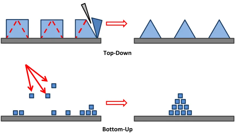
A wide range of different techniques has been developed for the fabrication of functional nanostructures. These processes are normally categorised as either ‘top-down’ or ‘bottom-up’ [1]; the underlying concepts behind the two are depicted in
Figure 1.1. Top-down procedures construct features using micro- and nanoscopic equivalents of traditional fabrication techniques like lithography, milling and
stamping [2]. This approach has proven incredibly successful: In fact, much of the modern computer era owes its success to the use of top-down manufacturing in the semiconductor industry. However, they tend to become increasingly challenging at
Top-Down
[image:27.595.113.524.67.300.2]Bottom-Up
26 smaller size scales and ultimately are unlikely to be feasible at sub-nanometre dimensions.
In contrast, the bottom-up approach aims to manufacture features through the piecing-together of smaller components, called ‘tectons’ [3]. This is directed by their
fundamental interactions with one another, which, through careful consideration of the tecton’s composition and the fabrication conditions, can occur in an autonomous manner without the need for external stimuli. Such ‘self-assembly’ results in highly
ordered structures with comparatively little manufacturing effort and thus is potentially an extremely powerful tool in surface engineering.
For self-assembly to be an effective route to nanostructure fabrication, it is essential that it is sufficiently versatile to construct functional materials into highly specific structures. In this respect, self-assembly of molecular tectons is perhaps the most attractive option. First, given the wealth of expertise developed over the last century, organic synthesis is now capable of manufacturing chemicals with a
multitude of different functional properties. Second, supramolecular chemistry [3] has demonstrated how careful selection of the manner in which tectons interact and
their molecular structure can grant an exquisite level of control over their assembly in a way unachievable with other materials. This is largely due to the variety of different intermolecular interactions available to organic molecules, which can be
used with excellent effect to direct the assembly of 1-, 2- and 3-dimensional (1D, 2D, 3D) structures. Moreover, this also allows specific tailoring of the interactions to
the tectons exact purpose within their given application. For example, where a high degree of uniformity is required, assembly through hydrogen bonds (H-bonds) and van der Waals (vdWs) forces are ideal, as their innate reversibility enables the
27 tectons that form intermolecular covalent bonds can be used [5]. In some scenarios, incorporation of metallic species may be essential, which can be readily achieved
with coordination bonding [6]. All of these have been demonstrated for various molecules on different surfaces. Moreover, in some cases, multiple types of
interaction are available, with the exact type being dependent on the precise experimental conditions used. For example, temperature [7,8] and deposition rate [9] are just two of the many important parameters that must be considered.
To successfully use molecular tectons in surface engineering, it is important that rational and reproducible design and fabrication protocols can be developed.
Perhaps the simplest and most intuitive approach for this is one that simplifies the process into two key steps. First, the desired functional properties are considered and an appropriate molecular ‘core’ is designed and synthesised. Second, this core is
functionalised with peripheral moieties that direct the molecules to self-assemble in the desired way. In this manner, all of the information required for the system to
assemble into a functional nanostructure is programmed exclusively into the molecular species. However, for construction on solid substrates, this approach is
normally unrealistic as it is usually impossible to neglect the influence of the surface and its corresponding interaction with the adsorbates. In the particular case of metal supports, whose conducting nature is an essential component of many applications,
the interaction can be sufficient to completely transform the functional properties, the assembly and even the intrinsic structure of the tecton and the metal.
28 detailed understanding of the molecule-substrate interaction, so that its effects can eventually be incorporated into the design process described above.
1.2 The role of the substrate
The molecule-substrate interaction can be highly complex as, depending on
the particular system in question, it can encompass vdW, coulombic and covalent contributions. With respect to surface engineering, it is particularly critical to consider the strength of the interaction and its impact on the functional properties
and assembly of the adsorbed tectons. Where it is very weak, the molecule is only slightly perturbed by the underlying metal. It therefore retains much of its gas-phase
physical and electronic structure [10,11] and is likely to be still capable of its originally desired functional properties [12]. This is typically labelled physisorption. Conversely, where it is strong, the organic species is considered to be chemisorbed,
which often results in substantial conformational, chemical and electronic modifications to both the molecule and the surface. Furthermore, molecular diffusion
can also be compromised and the assembly of chemisorbed molecules can therefore be severely hindered. The distinction between these two labels is not well defined
and is based rather arbitrarily on the magnitude of the interaction strength. Consequently, it is perhaps of greater use to consider the possible implications to the tecton and the substrate when the two interact strongly. In the following section, the
different repercussions are outlined, where they are loosely defined as either ‘structural’ – those that concern the conformation and composition of the molecule
29 1.2.1 Adsorbate and substrate structural modifications
Unless a molecule is extremely weakly adsorbed or is significantly rigid, it
will undergo distortions upon adsorption that optimise its interaction with the substrate. In the mildest cases, only very small conformational changes are likely to
occur [13,14], which ultimately have little to no effect on the molecular assembly or its functional properties. In other instances, the effects can be profound. For example, as a candidate for conducting wires or interconnections in molecular
computing systems, poly-aromatic molecules are promising. For their successful implementation, the species has to be adsorbed upon, but lifted from, a metal
substrate, which can be achieved by incorporating bulky chemical moieties at their peripheries (see Section 1.4.1 for more details). However, the strong interaction between π-electron systems and metals can be sufficient to bend the aromatic moiety
away from the desired height to one much closer to the surface [15]. In doing so, the adsorbate’s electronic structure is significantly perturbed and is consequently no
longer suitable for the role of a molecular wire.
The metal support is also not immune to adsorption-induced conformational
changes, and these effects can often be quite radical. For example, where the molecule-surface interaction is sufficiently strong, metal atoms can be lifted out of the surface plane. Whilst this sounds relatively innocuous, the resulting stress can
severely modify the assembly of the adsorbates [14,16]. In more extreme circumstances, the surface can even undergo radical reconstructions, resulting in a
fundamentally different structure to that before molecular adsorption [17-19].
When sufficiently strong, the molecule-substrate interaction can also lead to chemical transformations in the adsorbate. In such cases, chemical bonds can be
30 modification of tectons are often not well defined, resulting in unpredictable products that can be difficult to identify even with exhaustive multidisciplinary
studies [21-23]. While such reactions are the basis of the extensive success of reactive metal surfaces in heterogeneous catalysis [24,25], it should clearly be
avoided when the goal is to transfer molecular functionality to a substrate.
On the other hand, controlled chemical reactions on surfaces can, in some situations, be a useful tool with which to fabricate the desired molecular species. For
example, it has recently been demonstrated that the reactivity of metals and annealing treatments can be used to form covalent bonds between appropriate
tectons, resulting in the formation of very large single-molecule species [5,20]. As adsorbates of such size cannot be easily prepared by other means, this is likely to become an important tool in surface engineering.
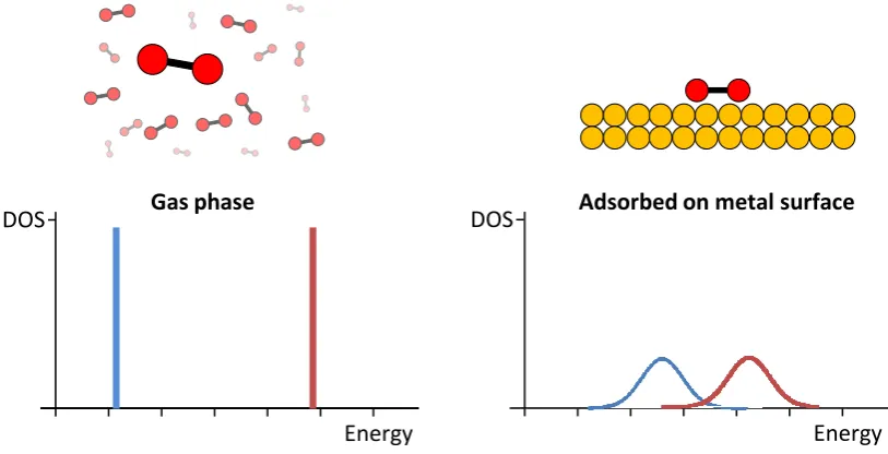
1.2.2 Electronic interactions between molecule and substrate An adsorbed molecule will experience a number of electronic perturbations
because of its proximity to a metallic surface. Perhaps the most difficult to predict a priori is the hybridisation of molecular and surface electronic states. When an organic tecton is adsorbed on a metal, the molecular and metallic electronic states are in close spatial proximity. If they are also sufficiently proximal in energy, the electronic structures of the two can mix, or ‘hybridise’. Metal surfaces exhibit a large
density of electronic states (DOS) over a wide energy range, and thus an adsorbate is always able to find electronic states with which to hybridise. The consequences for
31 1.2. In some cases this effect is relatively minor [11], but often the electronic
structure can be transformed beyond recognition [33].
In addition to this hybridisation are two effects that can shift the energy of an adsorbate’s electronic states. The first occurs upon electron transfer to or from the
molecule. When a charge is localised above the substrate (i.e. within the tecton), the electron density within the metal surface is redistributed. This results in an ‘image charge’ in the metal that, in terms of electron distribution and polarisation response,
is equivalent to an equal but opposite charge with respect to that in the adsorbed
species [34], as illustrated in Figure 1.3a. The coulombic attraction between the two charges stabilises that in the adsorbate, resulting in a reduced ionisation potential and an increased electron affinity. The net result is that the highest-occupied and lowest
unoccupied molecular orbitals (HOMO and LUMO, respectively), are typically shifted in energy towards the Fermi level, resulting in a reduction of the ‘molecular
Energy DOS
Energy DOS
[image:33.595.115.522.74.282.2]Gas phase Adsorbed on metal surface
32 band gap’ in comparison to that observed in the gas phase, as illustrated in Figure
1.3b.
In addition to the image charge effect, the formation of interfacial dipoles can also affect a tecton’s electronic structure. A number of different mechanisms can
occur that generate a dipole across the metal interface upon adsorption of an adsorbate, including charge transfer, chemical interactions and the image charge effect [35]. The net result is a constant electric field in the area immediately above
the metal in which the molecule resides. The electronic states of the adsorbate are rigidly shifted either upwards or downwards in energy by this potential, depending
on its sign, which is in turn determined by the direction of the interfacial dipole.
1.3 Characterising sample surfaces
Defining the role of the substrate in the self-assembly of organic tectons can be highly challenging. Moreover, ‘real-world’ metal substrates are already extremely complex, making the task of understanding the fundamental aspects of surface
engineering, in general, very difficult. With this in mind, surface science studies are
a) b)
Figure 1.3 a) Schematic representation of the adsorbate charge screening on metal surfaces. b) The HOMO-LUMO gap, labelled Eg, as a function of the molecule-substrate separation.
Eg Eg (red)
Energy
Height Height
33 typically performed using model systems, whereby the complexity of the molecule-on-metal sample is reduced by using simple, well-defined interfaces and molecules,
and precisely controlled experimental conditions. For example, many studies use highly crystalline substrates with low Miller index terminations, and make use of
ultra-high vacuum (UHV) systems. The latter grants exquisite control over the constituents of the surface throughout the investigation. Furthermore, many studies use relatively simple prototype tectons so that their adsorption behaviour, functional
properties and assembly can be readily understood within a limited number of experimental parameters.
Whilst model systems can greatly simplify the characterisation of functional surfaces, it is still often necessary to use a range of different experimental analysis techniques to construct a complete picture of a given sample. One of the most
important techniques, particularly when studying molecular tectons, is the scanning tunnelling microscope (STM). Since its invention in 1982 [36], it has revolutionised
the surface science field due to it being, until recently, the only technique capable of routinely imaging interfaces with sub-nm precision. This impact was recognised by
its near-immediate award of the physics Nobel prize in 1986 [37]. A detailed description of the technique is presented in Chapter 2. However, while it is an incredibly powerful technique, it cannot necessarily provide all of the required
information about a given sample. For example, STM does not directly provide details about the chemical state of an adsorbate, and thus many studies also make use
34 1.4 Controlling the molecule-substrate interaction
A very efficient way to control the effects of the molecule-substrate
interaction is the introduction of a gap between the two. In doing so, the adsorbate is protected from structural and chemical transformations and is also electronically ‘decoupled’ from the substrate due to the reduced overlap of their relative
wavefunctions. The magnitude of the separation is an important consideration; if the tecton is too close to the surface, some electronic interaction is still possible, whilst
if the separation is too great, charge transfer to and from the adsorbate via electron tunnelling is prevented. It is therefore necessary to aim for separations between these
two extremes, on the order of ~5 Å [31,38].
Perhaps the most succinct method for proving an adsorbate is fully decoupled is to quantitatively characterise its electronic structure. This can be achieved in a
number of ways, but scanning tunnelling spectroscopy (STS), a technique directly integrated into the STM experiment [39], is a particularly powerful tool for this as it
allows the simultaneous determination of a molecule’s local environment and its electronic structure.
The effectiveness of the combined STM/STS approach in this respect has been demonstrated numerous times [32,40-46]. In one particular example, a thin layer of NaCl was used to decouple individual pentacene molecules from a Cu(111)
surface [41]. When adsorbed on the bare metal, the STS spectrum of pentacene is featureless, due to the strong hybridisation of molecular and metallic electronic states
[33]. However, when located on top of the NaCl film, the pentacene STS spectrum shows strong peaks in both the occupied and empty states region (Figure 1.4a). Imaging the pentacene by STM at a bias voltage corresponding to these two peaks
35 resemble the HOMO and LUMO of the density functional theory (DFT)-calculated
gas-phase pentacene molecules (Figure 1.4b).
Strictly, the peaks observed in the STS spectrum do not actually correspond to the HOMO and LUMO of pentacene, but in fact to its positive and negative ion
resonances. The enhanced lifetime of the tunnelling electrons [41,47,48] in the pentacene results in polarization of the NaCl electronic structure underneath the
molecule, which in turn stabilises a partial charge in the pentacene. The resonances of the pentacene are thus slightly shifted in energy towards the Fermi level in comparison to the gas-phase molecular orbitals, as the electrons do not tunnel into a
neutrally charged species [49].
This effect can be used, in some circumstances, to control adsorbate charge
states; for example, adsorbed adatoms [50-52] and molecules [38,46] have been reversibly switched between different charge states. This increased charge stability
makes decoupled tectons promising candidates as bits for data storage applications, as switches in molecular electronics, and as activated precursors for tip-induced chemical reactions. STM-induced reactions are not exclusive to decoupled systems,
but controlled current pulses are normally required to initiate reactions. On
Figure 1.4 a) STS spectrum of pentacene adsorbed on top of a NaCl decoupling layer on Cu(111). b) STM images taken at the HOMO, Gap and LUMO voltages found in a). The DFT-calculated HOMO and LUMO of isolated pentacene are shown beneath, highlighting that the experimentally obtained images of the HOMO and LUMO exhibit similar spatial characteristics to the gas-phase species. Both images are adapted from reference [31].
36 decoupling films, charged adatoms have been bought into close proximity to molecules, which spontaneously react due to the charge on the adatom, forming a
metal-organic (MO) complex [43,44,48].
One particularly important application for decoupled tectons is in controlled
molecular luminescence. Luminescent molecules on conducting surfaces may prove to be highly efficient light sources; electrons can be pumped directly into the high-energy electron levels of adsorbates, resulting in an excited molecular state that can
in turn decay, emitting a photon. Furthermore, as the emitted photon is dependent on the fluorescing transition, stimulated photon emission has been suggested as a useful
tool in chemical characterisation [53,54]. However, emission from molecules on metal surfaces is often strongly quenched. The electronic coupling between the adsorbate and substrate electronic structures results in severe shifting and broadening
of the molecular energy levels and, consequently, the electronic states of the molecule are often no longer capable of luminescence [55]. In addition, the close
spatial proximity of a metal can strongly enhance the probability of non-radiative relaxation pathways that occur on a faster timescale than the photon emission
mechanism [53]. In particular, charge transfer of the excited electron into the empty metallic states can annihilate the molecular excited state, while strong coupling of the emitter’s dipole to surface plasmons may result in dissipation of the excitation
into the substrate [56]. These quenching mechanisms can all be inhibited by decoupling the adsorbate from the metal [54,57-59].
In the following, two main types of decoupling strategy are discussed in detail, so that the ‘ideal’ characteristics of an effective decoupling strategy can be ascertained. Other methods do exist, such as the use of lateral intermolecular
37 Consequently, the main schemes that are in principle applicable to a range of systems are presented below.
1.4.1 The ‘Lander’ approach to decoupling
Figure 1.5a shows the original concept behind the ‘Lander’ molecule [62], one of the earlier attempts at electronic decoupling that utilises a ‘self-decoupling’
approach. The Lander consists of a rigid core, from which the desired functional properties originate. The peripheries of the core are then functionalised with bulky moieties that act as ‘legs’, lifting the core from the surface, as illustrated in Figure 1.5b. The ‘Lander’ moniker comes from the specie’s notional resemblance to the
landing crafts used in interplanetary exploration [30].
Whilst the underlying principle of this approach is attractive, there remain a number of issues. One particularly difficult challenge to address is the way in which both adsorbate and the metal ‘react’ to the Lander core-surface separation. In a
manner of speaking, both adsorbate and metal are working to negate the hard-won electronic decoupling. First, although the Landers are designed to be rigid enough to
support the core, there is still often significant rotation and bending about the C-C bonds in the leg moieties [15]. The consequence of this, illustrated in Figure 1.5c, is that the molecular core is significantly closer to the surface than is desired and is
a) b) c)
Figure 1.5 a) Concept model for the ‘molecular Lander’. Adapted from reference [62]. b)
38 therefore not adequately electronically decoupled. Second, in some cases substrate adatoms can become trapped underneath the Lander [63,64], resulting in an effective
local reconstruction directly underneath the core that acts to increase the molecule-substrate interaction. The final and perhaps greatest limitation of the Lander
approach is that it imparts extremely strict limitations on the nature of the molecule. It must have significant rigidity if it is to maintain the electronic decoupling, as described above. This may preclude the inclusion of heteroatoms into the Lander,
which are usually strongly attracted to the metal surface. Additionally, inclusion of the leg moieties can potentially cause significant modifications to the desired
functional properties of the Lander core. Finally, the areas of the core where the legs are attached are effectively blocked, preventing the inclusion of other required peripheral functionalities, in particular those used to direct molecular assembly. In
other words, the functional moieties that direct assembly can only be included at the molecule termini, where there are no bulky chemical groups, and consequently the
Lander architecture limits directed molecular assembly to 1D [65,66].
1.4.2 Ultra-thin decoupling layers
An alternative approach is to use an ultra-thin film of insulating material – a ‘decoupling layer’ or ‘decoupling film’ – between the tecton film and the metal
surface, as depicted in Figure 1.6a. The use of inorganic materials has proven highly
successful in this respect. Such films can often be fabricated with the appropriate thicknesses and with sufficient band gaps [67], such that there is no electronic
39 unperturbed and as directed by their intermolecular interactions alone. The most commonly used materials are alkali halides and metal oxides, both of which are discussed in more detail below.
It is also possible, at least in principle, to achieve a similar decoupling effect using a multiple-layer thick film of the molecular tecton, as depicted in Figure 1.6b.
The first layer(s) act as a ‘sacrificial’ decoupling film, whilst later layers are sufficiently separated from the surface to be electronically decoupled [33,57,59]. However, this approach offers less control over the final product; the properties of
the sacrificial layer and the interaction between the different layers are not necessarily well defined.
1.4.2.1 Alkali halide decoupling films
Of the possible alkali halide options, NaCl has been by far the most popular
material choice for a decoupling layer. This is perhaps due to its simple internal structure and the relative ease with which suitably thick films can be fabricated on a range of different materials [31,69-74]. Furthermore, the growth of NaCl has been
optimised such that exclusively bilayer films can be formed on some surfaces [31,75], which is an ideal thickness for a complete electronic decoupling.
Figure 1.6 a) Schematic representation of the decoupling layer strategy. A thin layer of an insulating material is deposited onto the surface prior to adsorption of the molecular tecton. b) The ‘multilayer approach’ to decoupling, where a thick film of the organic species is deposited. The lower layers act as a decoupling layer.
40 The strong attraction between the ions within alkali halide films plays a critical role in their growth behaviour on surfaces. First, regardless of the substrate symmetry, alkali halides almost always form (100)-terminated films (shown in
Figure 1.7a). Only one example of a non-(100) film has been reported, which was only obtained after a considerably complex synthesis [76]. Second, alkali halide films exhibit a ‘carpet-growth’ regime: As the film grows laterally on substrate
terraces, it will encounter steps, which it spreads over smoothly to continue growth on the following terrace [69]. This is illustrated in Figure 1.7b. In doing so, the
alkali-halide maintains its (100)-termination. Finally, one study reported that when NaCl is deposited onto a particularly highly stepped surface, the underlying metal is
forced to reconstruct in a way that provides a better epitaxy for the NaCl (100) facets [71,77].
Figure 1.7 a) Side-view schematic of a NaCl bilayer decoupling film. The substrate is shown in grey, the Na ions are blue, the Cl in green, and the decoupled molecules are shown as red dumbbells. b) Depiction of the ‘carpet’ growth of NaCl over Ge(001), adapted from reference [69]. The substrate atoms are shown with partially shaded circles, the fully shaded circles show the Cl-ions within the NaCl structure.
a)
41 It is perhaps unfortunate that other alkali halides have received very little attention in comparison to NaCl, as the electronic states of adsorbates on NaCl have
been reported to be slightly broader than that expected [41]. This is not due to a residual molecule-substrate electronic coupling, but in fact arises from that between
the molecular electronic states and phonons in the NaCl film [78]. In contrast, when RbI films are used, this broadening is not observed, allowing normally obscured electronic features to be revealed [42]. It is not clear if this effect extends to other
alkali halide films due to their limited study.
1.4.2.2. Metal oxide decoupling films
Thin films of metal oxide on metals were originally studied as models for the substrates used to support catalytic metal dispersions [79]. As such films are both chemically inert and develop appropriately large band gaps within a few layers
thickness [67], they are also suitable candidates for adsorbate decoupling. In fact, a number of studies have already demonstrated their effectiveness in this regard
[54,58,80,81].
The most commonly used metal oxide decoupling film used is the surface
oxide of NiAl(110). By annealing the (110) termination of a NiAl crystal in an O2
atmosphere, approximately half of the substrate becomes covered with a 0.5 nm thick oxide layer [82]. The oxide has a highly complex structure and composition,
which has remained controversial until recently [82-84]. Other oxides have been explored, but their preparation is typically more complex; metal atoms need to be
deposited onto the sample using thermal deposition procedures whilst a background pressure of O2 is maintained [74]. For films grown in this way, a lack of good
42 growth [79]. In comparison, the NiAl(110) surface oxide has a reportedly low defect density and exhibits epitaxial growth along one direction [82].
The imperfections in oxide films are possibly their greatest limitation towards their widespread use. This is because defects usually interact relatively
strongly with overlayer adsorbates, in turn modifying their functional properties. Even on the NiAl(110) surface oxide, the effect can be quite pronounced. For
example, STS investigations of adatoms [68,80], metal clusters [85,86] and molecules [54] deposited onto this film reveal that the electronic states of the adsorbates can vary significantly, as shown by the STS spectra in Figure 1.8,
depending on their position with respect to the film. This is taken as evidence for adsorbates coupling to different defects in the film, although this is challenging to
prove given the difficulty encountered when trying to atomically resolve the surface of the oxide film with STM.
It is important to note that the use of inorganic layers in ‘real world’ applications will ultimately require that their growth conditions are well optimised.
a) b) c)
43 The low diffusion barriers of overlayer species, coupled with a preference for adsorbing on, or as near as possible to the metal surface [87-89] could result in
differently decoupled adsorbates if non-uniform decoupling layers are used. This can be avoided by ensuring that the decoupling film covers the entire surface and is of uniform thickness.
1.4.3 Organic decoupling layers
As an alternative to inorganic decoupling layers, films of vertically-standing
organic molecules are promising candidates [90]. In general, their properties are much more flexible, being easily tuned to their particular application through modifications to the molecular structure. To demonstrate this, the organic film can be
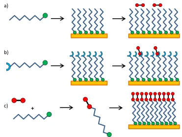
considered in the context of a simple three-part model [91], which is illustrated in Figure 1.9.
At one terminus of the molecule is the ‘head group’ that binds to the metal.
The strength of its interaction with the surface governs the films stability and the lateral mobility of each molecule within the film. Given the basic requirements of a
decoupling film, it is desirable that the moiety binds sufficiently weakly such that the film can self-assemble with a low defect density, whilst still being adequately Figure 1.9 Three component model demonstrating the versatility of organic decoupling layers. The head and tail groups control the interaction between the decoupling layers and the substrate and overlayer adsorbates respectively. The backbone controls the thickness and the rigidity of the organic layer.
Tail – tailors interaction with overlayer
Backbone– tailors film thickness
44 anchored to prevent lateral displacement by overlayer adsorbates. Consequently, the head group has to be specifically tailored to the substrate being used.
At the other terminus is the ‘tail group’, which points away from the metal. The ‘organic surface’ created by a densely packed decoupling layer will consist of
entirely this moiety, and therefore it determines the ultimate interaction with any overlayer adsorbates. With this approach, it should be possible to directly control the adsorption and assembly of overlayer species. For example, by using weakly
interacting moieties, any perturbations to the overlayer assembly can be limited, if not prevented, allowing tecton-defined assembly to occur. In contrast, moieties that
interact strongly with other organic molecules could be utilised in order to systematically modify overlayer assembly.
The final part of the model is the ‘molecular backbone’, which binds the two
termini together. The backbone defines the thickness of the decoupling film and, consequently, the separation and resulting electronic interaction between the
overlayer and the metal surface. It is also partially responsible for determining the packing of the molecular film. For example, long linear backbones in a
vertically-standing monolayer can result in a highly crystalline film structure due to strong vdW attractions [91]. It may also be possible to modify the monolayer’s structure by including assembly-directing moieties into the backbone. However, it is important to
note that the film packing is dependent on a number of factors, including the identity of the head and tail groups, and steric influences.
By far the most well-known example of vertically standing organic films are alkanethiol monolayers on Au(111 . Their prominence is such that the term

![Figure 2.6 Mean free path of electrons as they travel through an inorganic lattice.Adapted from reference [12]](https://thumb-us.123doks.com/thumbv2/123dok_us/9570124.461154/76.595.143.463.70.349/figure-mean-electrons-travel-inorganic-lattice-adapted-reference.webp)

