Surface Integrity in Micro-Hole Drilling Using Micro-Electro Discharge Machining
Hwa-Teng Lee
1, Werner P. Rehbach
2, Tzu-Yao Tai
1and Fu-Chuan Hsu
11Department of Mechanical Engineering, National Cheng Kung University, 701, Tainan, Taiwan, R.O. China 2Central Facility for Electron Microscopy, RWTH -Aachen, D-52056, Germany
This paper presents an investigation into the drilling of micro-holes of diameter 0.3 mm in tool steel H13 by means of the Micro-EDM process. Scanning Electron Microscopy (SEM) and Scanning White Light Interferometry (SWLI) techniques are used to determine the influence of the drilling process parameters upon the surface roughness. The results reveal a series of randomly overlapped craters upon the machined surface, which represent the position and chronological sequence of individual sparks during the machining process. As the voltage and current increases, the crater appearance changes from a conical to a cylindrical shape, and its depth and diameter both increase. It is shown that surface roughness deteriorates as the pulse voltage increases. Finally a regression equation is established between the diameter of the crater and the pulse voltage, pulse current and pulse-on duration parameters. This equation enables the diameters of the craters, and hence the surface integrity of the machined surface, to be predicted for a given set of process parameters, and is therefore a valuable tool in achieving the goal of precision machining.
(Received August 25, 2003; Accepted October 31, 2003)
Keywords: micro-electro discharge machining, surface integrity, surface roughness, crater, regression
1. Introduction
The continuing technological advances in micro-electro-mechanical systems (MEMS), electronic, medical and aero-space industries require a corresponding development of high-precision machining processes. The micro-scale com-ponents commonly associated with these industries demand increasingly fine fabrication tolerances and improved surface integrity. Accordingly, high-precision machining technology is becoming an increasingly important area of research.1–4)
Micro-Electro Discharge Machining Micro-EDM is one example of a high-precision machining process. It is a particularly important process since its application is uncon-strained by the hardness or material strength of the material being machined. Furthermore, since no direct contact occurs between the electrode and the machined component, no contact forces are induced during the machining process. Although the theory underlying the Micro-EDM process is the same as that which governs the conventional EDM process, an important difference between the two processes is that Micro-EDM adopts a switching circuit and an RC
circuit5–7) in order to lower the pulse energy, thereby
improving the machining precision.
Achieving a lower surface roughness is a prerequisite to improving machining precision, and this can only be obtained by improving the surface integrity of the machined product. Therefore, the role of the electric spark within the Micro-EDM process is fundamental since it affects not only the material removal rate, but also the depth of the heat-affected layer and the surface integrity. Accordingly, it is necessary to develop a complete understanding of the characteristics of the spark and the resulting surface integrity in terms of their dependence upon the machining parameters.
However, observation and measurement of the electric sparks during the actual machining process are virtually impossible since they are very small, exist only for a very short period of time, and are surrounded by a dielectric fluid. Therefore, it has been assumed that the characteristics of a crater formed by a single discharge can be used to determine
the properties of the forming spark. Many researchers have opted to conduct their studies on the basis of a single spark. Of these researchers, Ikai and Hashiguch8)adopted Heat Transfer theory to simulate the formation of the crater, and investigated the relationship between the heat source radius
and the crater radius. Meanwhile, Klocke and Noethe.9)
measured the spark temperature, and established its boundary condition in order to simulate the thickness of the heat-affected layer, the value of the residual stress, and the microstructure characteristics associated with the single spark. Finally, Karden10)used an AFM technique to observe the shape of the crater, and established the relationship between the process parameters and the shape, volume and diameter of the crater.
In the EDM process, material is removed as a result of a series of electrical discharges during a pulse-on duration. In practice, the spark originates at the point of the electrode which is closest to the workpiece at that moment. Accord-ingly, the precise position of each spark is random and cannot be predicted. Consequently, investigating the effects of a single spark is useful in developing an understanding of the basic mechanisms at work in the EDM process, but does not truly reflect the actual physical process.
As stated previously, the pulse energy associated with the Micro-EDM process is substantially less than that applied in the traditional EDM process. Accordingly, an observation of the machined surface reveals less molten material and reduced spraying from neighboring discharges. Although it is noted that the craters still tend to overlap each other, individual craters may be clearly distinguished. A single crater is formed by a single spark, and therefore, many sparks will form many craters. In other words, an observation of a series of sparks will provide some indications of the mechanisms operating within the actual physical process. Therefore, the current study investigates the relationship between the Micro-EDM process parameters and the result-ing surface morphology, surface roughness and crater shape and dimensions.
2. Experimental Procedure
This study uses H13 tool steel, which has previously been quenched and then tempered twice. In order to promote the efficient removal of debris from the machined surface, and to avoid the occurrence of secondary discharges, a hollow electrode is employed with an external diameter of 300mm
and an internal diameter of 130mm. During the machining process, the electrode is established as the cathode, while the tool steel sample serves as the anode. Micro-holes of depth 3 mm are drilled using an EMT 1.10 Micro-EDM machine (AGIE) with Held Oel IME 82 as the dielectric fluid. The effects of drilling parameters are investigated by applying pulse voltages of 100 V, 150 V and 200 V, pulse currents of 14 mA, 26 mA, 48 mA, 65 mA and 130 mA, and pulse-on durations (i.e. ON-times) of 5ms, 15ms, 30ms, 50ms and 100ms. The duty factor is set to be 0.15 throughout.
Since the aspect ratio of the drilled micro-hole, which is defined as the ratio of depth to diameter, is very large, it is impossible to observe its sides or bottom using any instru-ment. Therefore, each micro-hole is ground until the sectioned hole becomes clearly visible, and Scanning Electron Microscopy (SEM) is then used to examine the surface integrity. Subsequently, the surface roughness is measured using Scanning White Light Interferometry
(SWLI) at a1000magnification and with a depth of field
of 20mm. Surface roughness measurements are conducted at five different locations within a 72mm54mmarea of each specimen. Finally, the surface craters are observed using Scanning White Light Interferometry with the settings described above. The depth and diameter of four of the overlapping craters are measured. Note that the measurement activity is carried out on the four craters whose shapes are most complete, and which are located on the top surface of the overlapping craters. SAS statistical software is then used in an attempt to establish regression equations between the drilling parameters and the crater dimensions.
3. Results
3.1 Surface topography
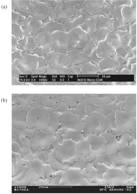
Figure 1 presents the typical surface topographies of micro-holes drilled using the Micro-EDM process. It can be seen that both topographies exhibit similar features to those commonly identified with the conventional EDM process, namely fused structures, debris globules, shallow craters, pockmarks and voids. However, as shown in Fig. 2, the morphologies of the Micro-EDM and conventional EDM processes are not precisely the same. The conventional process employs a very high discharge energy, which results in significant melting and vaporization of the workpiece surface. The molten material is swept away by the dielectric and may be re-deposited elsewhere on the surface, where it subsequently re-solidifies. Furthermore, each position on the surface may be machined by a series of several sparks rather than by one individual spark. This causes the shape of the surface craters to be less distinct, and the morphology to become more uniform. In contrast, the Micro-EDM process uses a substantially lower discharge energy. Therefore, less molten material is generated, and the width and depth of the
craters on the machined surface are reduced. The molten metal that is not flushed away by the dielectric undergoes rapid solidification and, as shown in Fig. 3, forms an evenly distributed series of overlapping craters on the EDMed surface. Although the craters formed by individual sparks are overlapped, it is still possible to identify the position and sequence of each successive discharge.
3.2 Surface roughness
As shown in Fig. 4, for constant pulse voltages of 150 V there is no obvious relationship between the surface
rough-(a)
(b)
Fig. 1 Surface Topography of Micro EDM. (a) voltage 100 V, current 14 mA, ON-time 5ms. (b) voltage 150 V, current 14 mA, ON-time 30ms.
[image:2.595.311.541.73.398.2] [image:2.595.313.541.442.608.2]ness of the machined surface and the pulse current or pulse-on duratipulse-on parameters. In other words, a reduced pulse current or pulse-on duration does not absolutely guarantee an improved surface roughness. One reason for this is that the entire machined surface is covered with craters, whose shape and dimensions under the same set of parameters are very similar due to the reduced pulse energy associated with the Micro-EDM process. In fact, it is the sequence of the randomly overlapping craters and not the crater shape or dimensions which plays a more significant role in determin-ing the surface roughness characteristics. Another possible reason for the apparent lack of influence of the pulse current and pulse-on duration could well be that the roughness is only measured within a very small physical area of the machined surface, and is performed at a high level of magnification, which further restricts the area of measurement. Furthermore, only four craters are examined within each measurement area. As a consequence, it is possible that the crater measurements taken are not truly representative of the entire machined surface.
It has been reported previously that the influence of the pulse voltage parameter is more significant than that of the on duration. Figure 5 confirms that for a constant pulse-on duratipulse-on of 30ms, the surface roughness decreases as the pulse voltage is reduced.
[image:3.595.53.284.72.227.2]3.3 Craters
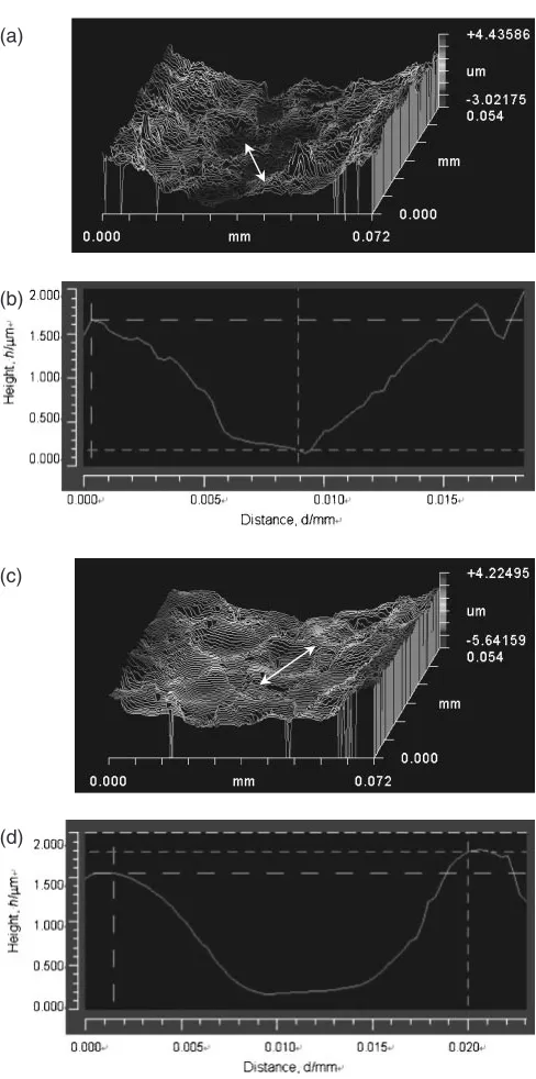
Figure 6 presents typical Scanning White Light Interfer-ometry profile and three-dimensional images of craters Fig. 3 Position and chronological sequence of individual sparks. (from 1 to
6) (Voltage 100 V, current 14 mA, ON-time 5ms).
0 0.1 0.2 0.3 0.4 0.5 0.6
5 15 30 50
Pulse-on Time, t /µs
Surface Roughness,
Ra
/
µ
m
14mA 26mA 48mA 65mA
Fig. 4 Surface Roughness for the voltage of 150 V.
0 0.1 0.2 0.3 0.4 0.5 0.6
14 26 48 65
Pulse Current, I /mA
Surface Roughness,
Ra
/
µ
m
100V 150V 200V
Fig. 5 Surface Roughness for the pulse-on duration of 30ms.
(a)
(b)
(c)
(d)
[image:3.595.318.536.74.203.2] [image:3.595.305.549.256.747.2] [image:3.595.61.279.276.407.2]formed on the machined surface. The images indicate that even in the same sample when the drilling parameters remain constant, the shape of the various craters will not identical. This observation can be attributed to the various interactions which occur between the dielectric circulation, debris, successive sparks, etc. It also indicates that the general shape of the craters changes from a conical to a cylindrical shape when the pulse voltage and current are increased.
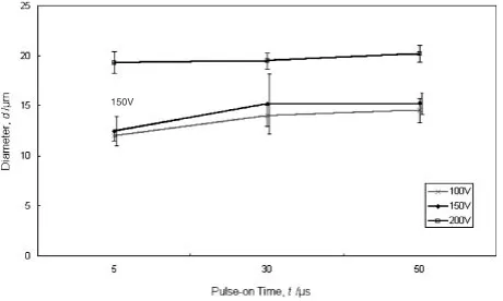
The shape of the crater depends on its diameter and depth, and determines the material removal rate. Figures 7 to 10 present the relationship between the crater dimensions and the pulse-on duration for various values of pulse current and pulse voltage. It can be seen that an increased pulse voltage results in a significantly higher crater diameter as shown in Fig. 7, and that the diameter will also increase slightly for a higher pulse current as indicated in Fig. 8, and an extended pulse-on duration as revealed in Fig. 7 and Fig. 8. Further-more, it is noted that an increased pulse voltage results in a greater depth of the crater when a pulse-on duration of less than 30ms is employed, but that the depth of the crater will subsequently decrease as the pulse-on duration is extended an shown in Fig. 9. For a constant pulse voltage of 150 V, when the pulse-on duration is less than 30ms the crater depth associated with a pulse current of 130 mA is smaller than that of pulse current 14 mA, but becomes larger when the pulse-on duratipulse-on is increased to lpulse-onger than 50ms as indicated in Fig. 10. Previously, it has been reported that an elevated pulse current will increase plasma channeling, hence low-ering the material removal rate.11) The current results are consistent with this finding.
4. Discussion
The results presented above have revealed that the most significant characteristic of a surface machined using the Micro-EDM process is the presence of a series of overlapping craters. Each crater is the result of a single discharge, and can be separately identified. Therefore, the observation of many randomly overlapped craters on the machined surface can be taken to represent the sequence of sparks associated with the actual Micro-EDM manufacturing process.
The results show that an increased pulse voltage will roughen the surface, but that the pulse current and pulse-on duration parameters have little obvious effect upon surface roughness. Further observation of the machined surface shows that the craters are randomly overlapped, and that they are very similar in shape and dimension for a constant set of machining parameters. Consequently, it can be concluded that surface roughness is influenced primarily by the extent to which the craters accumulate one of top of each other, rather than by their shape or size. However, this stacking effect appears to have no direct relationship with the machining parameters, and therefore the surface roughness cannot be predicted by considering each parameter alone.
When statistical regression techniques are applied to establish the relationship between the crater dimensions and the machining parameters in the range of voltage from 100 to 200 V, current from 14 to 130 mA, pulse-on duration from 5 to 100ms, it is found that an expression for the crater depth cannot be determined because of its low R-Square value. However, the R-Square value of the crater diameter is
150V
Fig. 7 Diameter of Crater for the pulse current of 14 mA.
[image:4.595.55.285.73.211.2]130mA
Fig. 10 Depth of Crater for the voltage of 150 V.
130mA
Fig. 8 Diameter of Crater for the voltage of 150 V.
150V
[image:4.595.314.542.74.210.2] [image:4.595.313.541.247.388.2] [image:4.595.55.285.255.389.2]0.72, and the corresponding regression equation is calculated to be of the form:
Diameter of Crater = 4.85 + 0.066 Voltage - 0.054 Current + 0.022 Duration.
5. Conclusion
The present study has investigated the use of the Micro-EDM process in the drilling of micro-holes in H13 tool steel. The main conclusions of the present investigation may be summarized as follows:
(1) The Micro-EDMed surface shows the presence of an evenly distributed series of randomly overlapping craters. Each crater may be individually identified, and indicates the exact position and chronological sequence of a series of discrete discharges.
(2) Of the various process parameters, the pulse voltage parameter exerts the greatest influence upon the surface roughness. However, surface roughness is determined primarily by the stacking effect of craters one upon each other rather than by the dimensions of the individual craters.
(3) The shape of the crater changes from conical to cylindrical as the pulse voltage and current increases. Furthermore, at elevated pulse voltages, both the diameter and the depth of the crater increase. Mean-while, an increased pulse current only results in a slight increase in crater diameter.
(4) A regression equation is established to relate the crater
diameter and drilling parameters in the form of: Diameter = 4.85 + 0.066 Voltage - 0.054 Current + 0.022 Duration. This equation enables the diameter to be predicted for specific drilling parameter values, and therefore enables the goal of precision machining to be achieved.
REFERENCES
1) D. M Allen:Demonstrated Micromachining Technologies for Industry, (IEEE Seminar, 2000) pp. 6/1-6/4.
2) T. Masaki, K. Kawata and T Masuzawa:Micro Electro Mechanical Systems 1990, (IEEE, 1990) pp. 21-26.
3) H. Li and S. D. Senturia: Electronics Manufacturing Technology Symposium, (Thirteenth IEEE/CHMT International, 1992) pp. 145-149.
4) D. Reynaerts, P. Heeren and H. Van Brussel: Sens. actuators. A Phys.
60(1997) 212-218.
5) T. Masuzawa, M. Fujino, K. Kobayashi and T. Suzuki: Bull. Jpn. Soc. Precis. Eng.20(2) (1986) 117-120.
6) O. Koch, W. Ehrfeld, F. Michel and H. P. Gruber: Proc. 13th International Symposium for Electromaching, (2001) pp. 737-745. 7) T. Masuzawa: Proc. 13th International Symposium for Electromaching,
(2001) pp. 3-19.
8) T. Ikai and K. Hashiguchi: Proc. 11th International Symposium for Electromaching, (1995) pp. 163-170.
9) F. Klocke and T. Noethe: Prod. eng. (1996) 29-32.
10) A. Karden:Funkenerosive Senkbearbeitung mit leistungssteigernden Elektrodenwerkstoffen und Arbeitsmedien, Dissertation RWTH Aa-chen, (Shaker Verlage, AaAa-chen, 2001) p. 49-60.