Increasing the bit density of a quantum
confinement physically unclonable
function.
By
Hamzah Shokeir
Department of Physics
Lancaster University
September 2017
Declaration
This thesis is the result of work carried out at Lancaster University between October 2016 and September 2017 and in collaboration with IMDEA Nanosciencia. I declare that the work presented was carried out solely and contains nothing which is the result of work done in association with others, except as specified in the text and references. The thesis is not substantially the same as any I have already submitted, or that I am in the process of submitting, for any degree at any university. This thesis does not exceed 30,000 words.
H.Shokeir,
Lancaster,
“Beautiful is what we see, more beautiful is what we know. Most beautiful is by far, what we don’t”
-Nicolos Steno
Acknowledgements
I would like to start by thanking my supervisor Prof. Robert Young who has given me the rare opportunity to embark on scientific research. His generosity, expertise and work ethic is an example for me to follow throughout my scientific career. This has been by far the most valuable year in my scientific and academic life and I am forever grateful for such.
I extend my thanks to our collaborators at IMDEA Nanociencia; Daniel Granados Ruíz and Manuel Rodríguez Osorio who made this project possible, I am forever indebted for their time and effort and for facilitating a huge part of this research.
Much of the achievements and attainments would not have bene possible without the help and support of Ramon Benardo-Gavito who has been a great mentor this year and a source of inspiration at times. And Thomas McGrath who put up with my dim moments and was one of the kindest individuals to work with. You are both great scientists thank you to both of you, not all heroes wear capes!
Thank you Chris Woodhead for assisting me in the helium flow cryostat setup, thank you Yassir Noori for assisting me in the SEM imaging and saving my hide in the last minute. Thank you Yameng Cao for useful discussions in understanding conceptual elements of the project. Thank you Ben for helping me out with the code. Thank you Johnny Roberts for getting me started into the project.
Summary
This dissertation presents work carried out in collaboration with the IMDEA nanoscience institute. We study the recently proposed quantum confinement physically unclonable function by Roberts, et al. that utilises resonant tunnelling diodes (physical representation of a quantum well) and atomic scale imperfections for applications in cryptography and identification. Presently such entities rely on their resonance peak position as the basis for a new approach to electronic identification systems.
By solely relying on the resonance peak of these devices deconvolution outputs an average of 8 bits per device, concatenation of up to 16 devices outputs a satisfactory number of bits for applications in uniqueness. However we explore the possibility of increasing the bit density of such physically unclonable functions that range from tangibly modifying the heterostructure with the use of a focused ion beam to induce quantum effects of 1 dimension (quantum wire) and 0 dimension (quantum dot) that would manifest its self as multiple resonance peaks observed on the current/voltage characteristic.
Our findings show multiple devices with consistent new features as a result of modification with the focused ion beam ultimately increasing the bit density. We carry out cryogenic measurements and comment on the fact that such features are not supported by previous work studying resonant tunnelling in the 1 & 0 states of double barrier heterostructures.
Table of Contents
Declaration ... 2
Acknowledgements ... 4
Summary ... 5
Chapter 1- The need for unique identities and increased bit density. ... 8
1.1 Introduction ... 8
1.2 utilising physical disorder ... 8
1.3 Digitisation of RTD. ... 11
1.4 Advancements and prospect. ... 12
1.4 Current work and contributions ... 13
Bibliography ... 15
Chapter 2- The Physics of Semiconductors and the QCPUF. ... 16
2.1 Introduction ... 16
2.2 Band structure, doping and III-V semiconductors. ... 16
2.3 Doping and Fermi level pinning ... 17
2.4 Density of states: quantum wells, wires and dots. ... 18
2.5 The Resonant Tunneling Diode ... 20
2.6 Fabrication of RTD. ... 22
2.7 The PUF, QCPUF and RTD. ... 22
2.8 The case of the strong PUF vs the weak PUF. ... 23
2.9 Resonant tunneling through higher order sates. ... 24
2.10 Temperature dependence of bandgap ... 26
Bibliography ... 28
Chapter 3- Experimental methods. ... 29
3.1 Introduction ... 29
3.2 Scanning electron microscopy ... 29
3.3 Focused Ion Beam ... 30
3.4 Electronic characterisation ... 31
3.4.1 Source measure unit ... 32
3.4.2 Room temperature probe station ... 32
3.5 Micro Wire bonder... 33
3.6 Low temperature measurements ... 35
3.6.1 Low temperature probe station ... 36
3.6.2 Helium flow cryostat ... 36
Bibliography ... 38
4.1 Introduction ... 39
4.2 Increased Bit Density ... 39
4.2.1-Introduction... 39
4.2.2-Etch designs and parameters. ... 40
4.2.3-Lateral etch. ... 41
4.2.4-Dimond etch. ... 43
4.2.4-Arrow etch. ... 45
4.2.5-Ring+Rectangle etch. ... 45
4.2.6-Ring+Triangle Etch. ... 47
4.2.7-Hole Etch. ... 49
4.2.8-Square etch... 51
4.2.9-Dot etch. ... 52
4.3-Analysis ... 54
4.3.1 Defective devices ... 54
4.3.2 Increased Bit rate ... 55
4.3.4 Minute features superimposed in NDR. ... 56
G1-Square etch. ... 56
F10-Square Etch ... 57
B4-Lateral Etch ... 58
4.3.5 Low Temperature Measurements of Bumps ... 60
4.3.6 Discussion and Conclusion... 63
Bibliography ... 65
Chapter 6 - Conclusions and Further Work ... 66
6.1 Conclusions ... 66
6.2 Further Work ... 67
Chapter 1- The Need for Unique
Identities and Increased Bit Density.
1.1 Introduction
When Francis Galton first developed his theory of fingerprints and physiognomy, few would have anticipated the impact in the modern world. It has been noted that Galton’s work contributed to the paradigm of absolute identification and that the biometric system is the absolute political weapon of the current era [1]. Today the use of fingerprints and biometrics is a corner stone of secure identification and security, the shift of our technologies advancing as well. Amidst the advancement of communication, financial transactions and the Internet of Things (IoT) the critical question of security lies behind every action. As we see the growth of such technologies in the coming years the cause for concern on the issue of trust is ever more great. Although we are now entering an era where advanced methods of cryptography are gaining much attention and spotlight in research (such as quantum cryptography). Counterfeit drugs contribute to a multi-billion dollar global business; according to a World Health Organisation study 450,000 people alone die annually in Africa as a result of fake malaria treatment [2]. It is not only a matter of technological importance but also of social, political and economic that our identification systems and methods guarantees a future without fakes.
Conventional systems of identification typically require the use of a key as the central entity for identification, such a key is usually stored digitally. The mere storage of a digital key in electronic hardware renders its self to attacks in cloning and learning [3]. What is required is a system that renders its self near impossible in cloning and attacking, it has been previously proposed that an entity that comprises of an inspirable link between its identity and physical structure would be an ideal candidate for assured identification [4].
1.2 Utilising physical disorder
The notion that we can utilise the physical atomic disorder in quantum nanostructures and other such structures such as 2D materials was first introduced by Roberts et al. [4] and Cao et al. [8] respectively. Optical tags analogous to that of a barcode found on a banknote can be comprised from 2D materials and their minute defects, such imperfections and defects can be introduced during the fabrication stage of crystal growth which can simply be spatial variations in the bandgap or the comparison of different monolayer and thicker layer regions of the tag [8]. In Cao’s work they were able to successfully characterise such imperfections from a transition metal dichalcogenide (TMDC), tungsten disulphide (WS2)via photoluminescence (PL) measurements and with the use of simple optics. Further tests with atomic force microscopy verified their measurements that the uniqueness was indeed a result of the nanoscale variations. The advantage of manufacturing atom thick optical tags that can be used as UOs is that they can be readily imbedded on the surface of products such as bank note or a pharmaceutical. Cao’s method provides a simple way to extract information based on the band pass filter orientation q, bandwidth Dw and the spatial variations from the PL measurements PL(x,y).
Figure 1.1b: A flake of WS2 showing a PL map of peak wavelength [8].
On the other hand, we are able to rely not only on the variations measured by optical characteristics such as those stated above, but also on electrical characteristics based on the same notion that imperfections on the atomic scale induce changes that we are able to visualise and measure to a high precision. In has also been shown that in Roberts’ work [4] that there exists an alternative to small scale optical practical PUF that can be implemented in everyday consumer life. However rather than relying on TMDC monolayer structures, Roberts’ work showed that it is possible to utilise certain types of quantum heterostructures that follow the same formula for a secure PUF; namely relatively easy to fabricate yet infeasible to clone.
A quantum heterostructure is defined as a structure typically comprised of multiple layers of semiconducting materials that are arranged in such a way that charge carriers are confined in a select number of dimensions. Confining electrons otherwise known as quantum confinement induces quantum effects within the system, namely that discrete energy levels are formed. However, the exact positions of these energy levels are subject to a number of uncontrollable parameters that are in effect during the fabrication stage of these heterostructures. It has been proposed that resonant tunneling diodes (RTDs) as a proof of concept of such a PUF [4]. What makes the RTD a favourable candidate in realising a secure PUF is that just as before where atomic disorder induced minute yet detectable variations in bandgap the same also applies when fabricating such quantum heterostructures. The barriers associated with the RTD are a few atoms thick, this intern causes minute atomic changes to contribute greatly to quantum confinement and tunneling.
The mechanisms in which we extract the uniqueness from the RTD is arguably simpler than the afore mentioned optical PUF, additionally the method of fabrication allows up to hundreds [9] of different PUFs to be fabricated at once.
Figure 1.2: (Left) SEM image of RTD 4x4 μm sized mesa. (Right) four RTD of varying mesa size displaying their IV characteristic.
To measure such, we simply require a voltage source and a way of measuring output current. Such a setup can take the form of a standard source measure unit (SMU).
However despite its many advantages over the optical PUF, a major disadvantage is that we currently only rely on one aspect of each device to extract its uniqueness, namely that each PUF only has one component of uniqueness. Regardless, each device acts as an entirely unique object and hence can be implemented as a quantum confinement PUF (QCPUF).
1.3 Digitisation of RTD.
Figure 1.3: a) Gaussian distribution showing the peak location in terms of bits(101, 011) given the axis are divided into 8 bins. b) Table showing the evolution of bins (k) with bits (b). c) Hamming distance of strings of bits from concatenated devices of current and voltage (22 devices, 256 bins), from [10].
The result of concatenation would increase the total number of bits to B, the number of devices required to output a total number of bits B, where each device contributes b bits is give by 𝜑 = 𝐵/𝑏. A sufficient number of bits ideally would be in the range of B=128. To achieve such one would require connecting multiple devices to extract multiple peaks, depending on the number of bins we assign per axis this would range from 16 to 22 devices. The tunneling region could also be used as a source of uniqueness as in principle is based on the same assumption that justifies our usage for the peak position. One could apply a linear regression that approximates a scalar term from the positive differential resistance then convert the scalar term to a binary sequence. However further investigation is required.
Given the advent of modern technology growing smaller and smaller the issue of scalability is not necessarily an immediate issue given the typical dimension of such devices however to realise a fingerprint like architecture of multiple minutia per sample we raise the problem: how are we able to extract more bits from a single device. Hence reducing the required number of RTDs to extract the ideal number of bits,
1.4 Advancements and prospect
Current fingerprint identification systems have advanced immensely since they were first implemented in forensics and other such fields. However, since their discovery and realisation in identification in the 1800s, the central concept on how we are able to extract uniqueness has remained the same throughout. During the verification phase a system scans the fingerprint for specific topographies known as minutiae. Such minutiae range from bifurcation to short ridges that randomly assorted on one’s finger. Our methods of detecting such minutia have become increasingly more and more advanced as magnifying lenses have been replaced with CMOS image sensors. Although there exist multiple standards for minutiae recognition and identification [11], a standard approach requires a system that measure the distances and the angles between the minutiae and uses an algorithm that converts such data into a numeric code or a string of bits (Fig 1.4).
a) b)
Figure 1.4: Schematic of how information is extracted from minutiae of fingerprint, mapped and digitised producing a string of binary data.
Generally the more fingers used, the greater the accuracy in identifying an individual and the greater number of minutiae used the greater the bit density of the extracted numeric code. Referring back to our analogy of using the IV peak position as a unique object similar to that of a fingerprint the question arises on how we can create further minutiae to maximise the complexity and hence increase the bit density of our QCPUF.
The central mechanism of the QCPUF is one dimensional quantum tunneling which relies on the presence of a quantum well heterostructure. We propose altering the structure in such a way that we create a greater dimensionality of confinement and hence have multiple resonance states that can be seen on the IV characteristic as multiple peaks. In order to create multiple confined regions, we must reduce the active area of the device significantly such that there is the presence of a quantum wire (2D) or quantum dot (3D).
1.5 Current work and contributions
Such raises the question of how one would embark on creating a structure with multiple confined states. Reengineering such structures from the fabrication stage is viable however we explore the possibility of modifying the structure post fabrication. We resort to the use of an etching process that allows us maximum control of not only the parameters but how we manipulate our etchant. We employed a focused ion beam (FIB) that allows us to alter the physical structure of our devices and aimed at introducing increased dimensions of confinement.
We explored up to 8 different etch designs with the FIB across over 69 devices. Our initial conclusions were such that designs that employed simple geometries that at the same time maximised the possibility of a confined active region produced the most interesting results. In essence, etching a square cavity (or similar) centred on the RTD mesa left constricted corners and lateral regions on the device. With said designs we observed consistent results that bare close resemblance to the results published by Tarucha Et al. [12].
we present only the IV characteristic under the negative bias, as generally broader peaks and larger PVR are observed under such bias. We also produced a set of devices whose final surface area was less than 4 μm2 (the current minimum of such RTDs) with a clear NDR region resulting in an increase in bit density per unit volume.
We begin the study by presenting the different designs for each etch type, in many cases the designs yielded non-functioning devices. Only a select few of the etch designs produced devices that were functioning post FIB and even fewer devices gave interesting results on the IV characteristic that were worth investigating.
We have stated the need for a new approach in how we identify our everyday objects, given the losses counterfeit products yield, methods that utilise intrinsic subatomic unpredictability have been proposed as an advanced means of security. Our proposition is to further utilise such features in a QCPUF and to create a fingerprint like architecture by introducing further minutiae.
Bibliography
[1] N. Lebovic, "Biometrics or the Power of the Radical Center", Critical Inquiry, 2015.
[2] K.Kaliyaperumal, “The Counterfeit Anti-Malarial Is a Crime against Humanity: A
Systematic Review of the Scientific Evidence,”
Malaria Journal,
vol. 13, 2014.
[3] A. B. L. K. I. &. N. D. Barenghi, “Fault injection attacks on cryptographic devices: theory,
practise and countermeasures,”
in Proc. IEEE,
vol. 100, p. 3056–3076, 2012.
[4] J. Roberts, “Using Quantum Con nement to Uniquely Identify Devices,”
Scientific
Reports,
2015.
[5] R. B. T. J. a. G. N. Pappu R, “Physical one-way functions,”
Science,
vol. 297, no. 5589,
pp. 2026-2030, 2002.
[6] S. F. S. ̈. J. D. G. D. S. a. S. J. Ru ̈hrmair U, “Modeling attacks on physical unclonable
functions,”
"Proceedings of the 17th ACM Conference on Computer and
Communications Security CCS” ,
p. 237–249, 2010.
[7] H. L. K. C. D. a. W. M. D. F. Konigsmark S T C, “Cnpuf: “A carbon nanotube-based
physically unclonable function for secure low-energy hardware design,”
9th Asia and
South Pacific Design Automation Conference (ASP-DAC),
pp. 73-78, 2014.
[8] Y. R. Cao.Y, “Optical identification using imperfections in 2D materials,” 2017.
[9] Missous et al., “Fabrication of Submicrometer InGaAs/AlAs Resonant Tunneling Diode
Using a Trilayer Soft Reflow Technique With Excellent Scalability,”
IEEE electron device
Letters,
vol. 61, no. 7, 2014.
[10] U. I. Bagci, “Generating Secrets From Quantum Confinement Physically Unclonable
Functions,”
In Press.,
2016 .
Chapter 2- The Physics of
Semiconductors and the QCPUF.
2.1 Introduction
We begin by drawing our attention to a brief summary on the physics of semiconductors and in particular how we utilise the phenomena of solid state structures to create entities such as tunnel diodes. In this chapter we will elucidate how quantum effects in semiconductor nanostructures can be exploited in cryptography in the form of a quantum confinement physically unclonable functions (QCPUFs) and provide the argument of how we are able to increase its bit density.
Central to our investigation is the resonant tunneling diode (RTD), a heterostructure that functions based on quantum tunneling. In particular it is the minute imperfections within the bandgap, interfacial roughness and doping profile of these semiconductors that yield the significant elements of our research. To reiterate as previously expressed; we are making use of atomic imperfections as a means of identification analogous to that of our fingerprint.
Although we do not contribute to any new theoretical discussions, we present the prerequisite literature to support our experimental findings later. We begin by reviewing the topic of the quantum theory of heterostructures, the effect of quantum confinement, band structure, the density of states and quantum tunneling. We will describe the roles of the semiconductor in our investigation and study the structure of quantum wells (QWs) and their application to double barrier resonant tunneling diodes (DBRTD) and their epitaxial growth. Furthermore we present the theoretical argument behind how physically altering such a structure will give rise to additional minutia and reference the initial studies of Reed et al.
2.2 Band structure, doping and III-V semiconductors
Our devices are primarily comprised of materials known as semiconductors, such materials exhibit useful properties in that at room temperature they are electrically conducting however they differ to regular conductors such as copper or zinc in that at absolute zero they in theory are completely insulating.
We recall that the outermost orbital structure of an atom consists of a lowest unoccupied molecular orbital (LUMO) and the highest occupied molecular orbital (HOMO), otherwise known as the conduction band and the valance band respectively. In conductors, these such bands overlap allowing for electronic and thermal transport. In particular our devices are comprised of elements that exist in groups III and V of the periodic table, such semiconductors are hence often referred to as III-V semiconductors, others such include III-Nitride and II-VII.
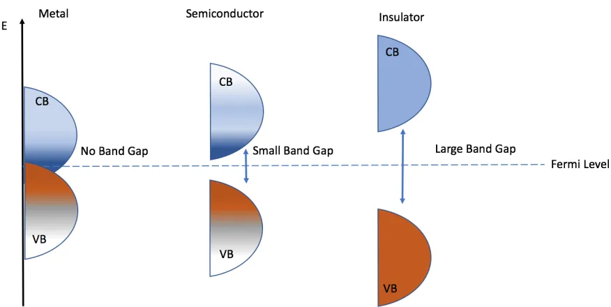
dispersion relation of electrons. Namely when the wavelength of the electrons propagating through the lattice is comparable to the lattice spacingk=p/a where k is the wave vector and a is the lattice spacing. In particular the electrons are reflected due to the varying potential of the lattice and form standing waves of different displacements by a/2. As a result, these standing waves have different energies known as bands, the spacing between these bands are termed bandgaps and are prominent in insulators and semiconductors. The highest energy band with the most occupied states is referred to as the valence band whereas the lowest energy band with least occupied states is the conduction band. Semiconductors host a bandgap minimal compared to that of insulators, electrons can be thermally excited from the valance band to the conduction band and are governed by Fermi-Dirac statistics. However at absolute zero the semiconductor behaves as an insulator as there exists no free electrons, the Fermi level is the highest energy occupied by electrons in a material at 0K.
Figure 2.1: Variation of bandgap in metal, semiconductor and insulator highlighting the conduction and valence bands. Insulators having the largest bandgap followed by semiconductors than metals.
2.3 Doping and Fermi level pinning
The intrinsic properties of semiconductors can be altered by introducing impurities, this process is known as doping and exist in two types of dopants: donors and acceptors. The elements used depend on the host material; acceptors are dopants that contain fewer electrons than the hosting material (p-type) and whereas donors are atoms that contain a greater number of electrons than the hosting material (n-type). With these subsequent doping types, acceptors typically have an unoccupied energy level (acceptor level) that is positioned above the valence band and donors have an unoccupied electron level that is positioned below the conduction band.
conductivity and can be due to surface effects, i.e. caused by the exposure to a gallium ion beam on the heterostructure surface.
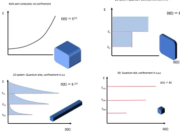
2.4 Density of states: quantum wells, wires and dots
We have thus far briefly touched upon the effects of quantisation and how such influences the formation of bands, however quantum confinement influences the bulk properties of the material in particular that the bandgap increases as the dimension of our sample decreases. We observe such effects when the physical dimensions of our system is of the order of the de Broglie wavelength.
𝜆 = ℎ
(𝑚∗𝑘 2𝑇)45&
Where KBis the Boltzmann constant, m* is the effective mass of the electron, h is Planck’s constant
and T is the temperature. The application of such in different structures is also of central importance in our understanding of how RTDs work. We classify structures based on their degree of confinement;
Three dimensional structure (bulk):- The dimensions of the structure are large such that there exhibits no confinement in any directions
Two dimensional structure (quantum well):- Confinement exists in one dimension (z) and the electrons are free to move in the x & y planes .
One dimensional structure (quantum wire):- Confinement exist in two dimensions (z, x) and the electrons are free to move in the y plane.
Zero dimensional structure (quantum dot):- Confinement exists in all three dimensions (x, y, z).
The order of confinement occurs (Fig 2.2) when the dimension of our structure is comparable to the de Broglie wavelength of the electron, also known as quantum box quantisation.
The Schrödinger equation which describes our system is extremely difficult to solve analytically, in particular when dealing with our system of heterostructures; approximate methods such as perturbation theory, quantum Monte Carlo, WKB approximation, etc. are the only means of solving such. The density of states (DOS) is defined as the number of allowed states within energy range. A general derivation for DOS in multiple dimensions is found in [1], however for convenience we present the subsequent dispersion relation for all four cases (Bulk, 2D, 1D, 0D).
Figure 2.2: Energy vs density of states (DOS) of 3D system (bulk), 2D (quantum well), 1D (quantum wire) and 0D (quantum dot) systems. The inset highlights the planes of confinement.
Given we are able to contrast and compare the different levels of confinement by comparing their density of states vs their confined states. If we now confine electrons in an additional dimension such that the electrons are restricted in two dimensions and are free to move in one we have effectively created a quantum wire structure. Further confinement to a third degree, now reducing the dimensionality of the free electron to zero creates a structure known as a quantum dot. A material that does not exhibit confinement in any dimension is simply referred to as the bulk and exhibits no quantum effects.
Structure Degree of Freedom Nanoscale dimension Density of States
Bulk 3 1μm
®
¥
𝐷𝑂𝑆9:(𝐸) = 8p√2 ℎ9 𝑚:?@
9 & 5
A𝐸 − 𝐸C
Quantum Well 2 1-1000 nm (thickness) 𝐷𝑂𝑆
&:(𝐸) = 4p ℎ&𝑚:?@
Quantum Wire 1 1-100 nm (radius)
𝐷𝑂𝑆4:(𝐸) = 2A𝑚:?@ √2 ℎ√𝐸
[image:19.595.112.479.87.361.2]Quantum Dot 0 1-10 nm 𝐷𝑂𝑆E:(𝐸) = 2𝛿(𝐸 − 𝐸C)
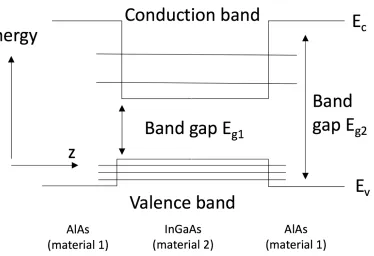
A quantum well structure can be replicated when combining a material of a wider band gap (i.e. GaAs) followed by a material of a narrower band gap (i.e. InGaAs) followed by the wider band gap material again; in our case a sandwiched layer of indium gallium arsenide (InGaAs) between two layers of aluminium arsenide (AlAs) was studied. The details of the fabrication method are discussed later in Sec 2.5, the growth of this heterostructure in the Z direction then forms a quantum well where electrons experience quantum confinement. The laws of quantum mechanics renders the electron subjected to confined subbands that are of discrete energy. The electron is still free to move in two other dimensions and behaves as it would in a two dimensional electron gas.
Figure 2.3: 2D confinement AlAs/InGaAs/AlAs quantum well showing the confined levels in the valence and conduction band. The rectangular shape is due to the perfect epitaxial growth.
Much of our attention will be centred on the quantum well, advancements in heterostructure engineering have enabled devices that utilise the effects of quantum confinement in the production of resonant tunneling diodes [3].
2.5 The resonant tunneling diode
We have demonstrated that quantum wells are the simplest of structures to exhibit quantum confinement. We now draw our attention to a particular diode that makes use of the property quantum tunneling in which the wave function of an electron has some finite probability that enables it to enter into a forbidden region due to its wave-particle characteristics. Tunnel diodes exhibit a characteristic negative differential region (NDR), the RTD follows a structure similar to that of Fig 2.3, in which material 1 forms the barriers and material 2 forms the well of confinement.
and resonates allowing the maximum rate of tunneling. Further increasing the voltage results in the first confined state becoming lower in energy and enters the region of the bandgap, transmitted current degreases. However further increasing the voltage will allow thermionic means of electrons to transmit.
Figure 2.4: Representation of the resonant tunneling process where a bias is applied and causes a shifting in the bands. 1) shows the structure at zero bias, 2) with some applied bias, 3) the Fermi sea coming in line with the first confined state 4) thermionic means of conduction occur.
Figure 2.5: IV characteristic of a RTD undergoing a bias highlighting the different stages of resonant
tunneling, where voltage is sourced and current is measured.
[image:21.595.69.348.444.652.2]2.6 Fabrication of the RTD
RTDs have been studied for decades, they were first discovered by [3], since then many groups have fabricated them using a wide variety of methods such as via reactive ion etching and electron beam lithography. The different methods vary in complexity and resources. The devices were fabricated by Missous et al. using a trilayer soft reflow method [5] which uses photolithography to laterally define the structure. The structure was grown in a RIBER V1000 molecular beam epitaxy (MBE) on an indium phosphate substrate.
It has been shown that monolayer variations in AlAs barriers yield a variation of 270% in the IV characteristics of RTDs [5]. Such variations are extremely difficult to govern and are often induced in the fabrication stage, additionally the position of the confined states are sensitive to the quantum well width, barrier height and well depth. When considering our heterostructure and their atomic make up, it is considered extremely infeasible to identically replicate two RTDs to near perfection [6].
2.7 The PUF, QCPUF and RTD
In this section we expand on the previously introduced concept of a physically unclonable function (PUF), we will also reveal how many of the fundamental concepts explored above can be exploited and used as a PUF. The notion of a PUF was initially introduced by Pappu et al. [8]. In the original publication it described that a PUF must be a physical unit that can be evaluated at great ease but impossible/infeasible to replicate despite infinitely advanced computational capabilities. Analogously one can view the PUF as a physical analogue of a mathematical one way function.
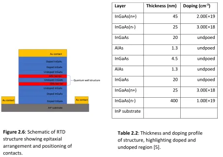
Layer Thickness (nm) Doping (cm-3)
InGaAs(n+) 45 2.00E+19
InGaAs(n-) 25 3.00E+18
InGaAs 20 undpoed
AlAs 1.3 undpoed
InGaAs 4.5 undpoed
AlAs 1.3 undpoed
InGaAs 20 undpoed
InGaAs(n+) 25 3.00E+18
InGaAs(n-) 400 1.00E+19
[image:22.595.75.534.187.510.2]InP substrate
Figure 2.6: Schematic of RTD structure showing epitaxial arrangement and positioning of contacts.
At the heart of every PUF is randomness, such can come in different forms and is paramount that under different conditions each PUF stays unique to itself. There exist PUFs who’s randomness can be explicitly induced by controlling and optimising specific parameters, such PUFs include optical PUFs and coating PUFs. There also exist PUFs that rely on intrinsic randomness. It has been previously suggested that other quantum systems can be used as PUFs, such as quantum dots [9]. Defects and disorder induced in the fabrication process can be observed when studying the variations in the optical spectra. Further detail of the mechanics of extracting the optical spectra from quantum dots for their use as a PUF can been studied in [6]. Recently is has been shown by Roberts et al. [9] that the resonance peak position of the IV characteristic of RTD can be utilised as such PUF. As mentioned above the fabrication process induces uncontrollable minute variations within the heterostructure. In Roberts’ work they investigated the uniqueness of such QCPUF and found little to no similarity of two RTDs.
Figure 2.7: (a) Different peak position of 26 identically manufactured devices showing a clustered region encircled in red. (b) Confidence regions of peak position from clustered region in (a). Inner most radius refers to 95%, middle region refers to 99.99% and outer most region refers to 99.997%. Taken from [9] with permission.
Further studies have shown that the QCPUF is extremely robust and can be a source of reliable uniqueness. The following section will review the suggested implementation of such.
2.8 The case of the strong PUF vs the weak PUF
UOs have been implemented on currency notes and documents of ID, however such can be more versatile and can be implemented in a wide range of applications such as key/random number generation. One method used in verifying a PUF is known as the challenge response pair (CRP); such requires the use of a secure database to host the exact CRP and to provide unique yet repeatable responses to the challenges.
Every CRP must be removed from the database after each use, the question of the security of such database is reserved for another study. Nonetheless another scheme suggests the use of a single CRP that rather than requires the use of a database, uses a certificate verified and hosted by the manufacturer [11]. PUFs also known as physically obfuscated keys (POKs) are a good example of a weak PUF. Both types of PUFs can be used in such a way that the responses are used in key generation and must abide by the CRP protocol such that in response to every challenge an output is generated that is unique and randomly dependant on the internal structure. Both PUFs are ideally stable under different moderate environmental conditions. Ideally a weak PUF is kept secure through implanted
PUF however allows an attacker to gain access to the PUF and to apply as many challenges and record as many reposes as they wish. However the attacker will have a near impossible chance at predicting the response for every given challenge even providing the attacker has sufficient amount of time due to the exponential nature of the complexity of the PUF.
Currently the QCPUF relies on the resonance peak position which has strong evidence backing its uniqueness which relies on confinement in one dimension, however to increase the complexity (and to increase the bit density) of our PUF we propose increasing the dimensionality of confinement to induce further resonance peaks that by deduction will be just as unique as they rely on similar mechanisms and conditions (i.e. atomic scale variations).
In [12], Bagci’s outlined a scheme of extracting binary information from such physical systems from their peak position. A Gaussian peak finding algorithm locates the peak position and divides the current and voltage axis into bins (Fig 1.3a). Each respective bin contains binary information and scales as the number of bins increase (Fig 1.3b). Per device the optimum number of bits extractable without influence of measurement fluctuation was k=256, such outputs 8 bits from the relationship
𝑏 = 𝑙𝑜𝑔&(𝑘)
where b is the number of bits and k is the number of bins. To obtain the more optimum 128 bits, Bagci followed a method of concentration where the total number of bits B (128) depends on the number of devices (j) and how many individual bits we are able to extract from each device, while keeping k constant (256); as 𝜑 = 𝐵 𝑏5 . From this it can been deduced that using an 8 bit sequence would require 16 concatenated devices, and a 6 bit sequence would require 22 devices.
2.9 Resonant tunneling through higher order sates
As we have pointed out previously, decreasing the physical dimensions of our bulk sample restricts the degrees of freedom of our electrons and induces confinement in other dimensions. A RTD visualises confinement in the 2D case, however in theory it is possible to visualise electron tunneling as a series of multiple resonant peaks in the 1D and 0D case by confining our system [12]. such gives rise to multiple resonance peaks visible within the IV spectrum. However to justify such an argument we reference the works of Reed Et al, S.Tarucha and M.Van Hove Et al. who conducted similar studies with different structures and for different applications. Their work nonetheless demonstrated the effect of resonant tunneling in 0D and 1D. Their results demonstrated clearly that their bumps were the result of lateral constriction of their heterostructures. Detailed theoretical descriptions concerning the underlying mechanisms were brought forward in subsequent publications. However Issues arise when modelling 0D tunnelling such as lateral mode mixing which varies on the uniformity of the confinement potential and the mixing of resonant tunnelling and Coulomb blockade single electron tunnelling effects.
The initial study by Reed et al. [12] fabricated narrow columns of AlGaAs/InGaAs and observed a series of resonant peaks attributed to RT in 0D. Observation of 0D states in AlGaAs-GaAs heterostructures laterally constricted by hydrogen plasma [11] present aligning results to Reed’s work.
Figure 2.8: (a) Representation of epitaxial structure containing a quantum well hosting multiple confined states due to 0D confinement, EcΓis the gamma point conduction band, R is the radius of the column. (b) confinement potential of a laterally constricted column, VLC(r) is the laterally confined potential. W is the depletion depth, the blue shaded region is the effective channel [14].
In Reed’s work electrons are laterally confined to a ‘gutter’ potential which is comprised of a flat and parabolic region. The fine peak structure found in Reed’s and in other cited work [12] were only visible at low temperatures.
A difficulty in modelling the behaviour of 0D tunneling stems from the non-uniform lateral confinement potential such results due to the lateral quantised energies varying steeply in the z dimension of the quantum dot. This is because the spacing of energy bands in the well is much greater than in the contact (emitter) region. In addition to this, the uneven confinement causes lateral-mode mixing of the wave functions. It was found by Reed et al. that the fine peak structure observed in the IV characteristic can be modelled as resonances of confined states within the well aligning with those in the emitter (conduction band). In Reed’s work the potential of the 0D structure was given by
Φ(𝑟) = ΦI[1 −LMN O ]&
Where r is the radial coordinate, R is the radius of the lateral column, ΦI is the potential height, W is the depletion depth. The authors also resolve the splitting of the quantised electron states as
∆𝐸 =ℏ 𝑅T
2ΦI 𝑚∗
Where m* is the effective mass in the well. Their measured value of state spitting is 25meV and matches closely with their expected value of 26meV.
(b) (a)
(3)
Figure 2.9: (a) Peaks in NDR region which correspond to tunneling through discrete states in the 1D & 0D structure measured at 4K. The arrows correspond to the calculated voltage positions of each state. Reprinted from [14] (b) Fine structure attributed to quantum box quantisation measured at 1.2K, where R is the varying diameter of the emitter contact. Reprinted from [13].
2.10 Temperature dependence of bandgap
Central to our clarification is studying the effect of temperature on semiconductor heterostructures. We conduct cryogenic measurements and observe changes of the peak and valley position. We also observe the prominence/broadening of such bumps within the NDR (Sec 4.3.5). Although a more rigorous theoretical evaluation of the effect of temperature on semiconductors is beyond the scope of this thesis. We briefly illustrate said effect by introducing Varshni's empirical formula which highlights the increase in bandgap energy with decreasing temperature. The formula is dependent on two constants (a and b), specific to the element that determine the relationship of bandgap energy and temperature.
𝐸U(𝑇) = 𝐸U(0) − a𝑇& 𝑇 + 𝛽
Where Eg(0), a and b are fitting parameters dependent on the material.
Si Ge GaAs
Eg(0) (eV) 0.7437 1.166 1.519
a (eV/k) 4.77E-4 4.73E-4 5.41E-4
b (k) 235 636 204
Table 2.3: Material constants for Varshni’s empirical formula, for Silicon, Germainum and Gallium Arsenide [13].
One can comment that at lower temperatures, the amplitude of atomic vibrations decrease which causes a smaller interatomic spacing and follows a trend seen in Fig 2.10.
(b) (a)
Figure 2.10: Variation of bandgap of GaAs with temperature showing an increase in bandgap as temperature decreases [16]
Bibliography
[1] C. S. H. &. V. A. Johnson, “Resistivity of Semiconductors Containing both Acceptors and
Donors,”
Phys. Rev,
vol. 79, no. 535, 1950.
[2] T. Heinzel, Mesoscopic Electronics in Solid State Nanostructures, 2 ed., Wiley-VCH,
2007.
[3] L. R.Tsu, “Tunneling in a Finite Superlattice,”
Appl. Phys. Lett,
vol. 22, no. 562, 1973.
[4] K. J. P. J. e. al., “A Dual-pass High Current Density Resonant Tunneling Diode for
Terahertz Wave Applications,”
IEEE Electron Device Letters,
vol. 36, no. 12, 2015.
[5] e. a. M. Missous, “Fabrication of Submicrometer InGaAs/AlAs Resonant Tunneling
Diode Using a Trilayer Soft Reflow Technique With Excellent Scalability,”
IEEE electron
device Letters,
vol. 61, no. 7, p. 2014.
[6] J. e. a. M. Missous, “Extremely Uniform Tunnel Barriers for Low-Cost Device
Manufacture,”
IEEE ELECTRON DEVICE LETTERS,
vol. 36, no. 6, 2015.
[7] M. K. e. a. C. Shao, “Achieving reproducibility needed for manufacturing
semiconductor tunnel devices,”
IEEE Electronic Letters,
vol. 49, no. 10, 2013.
[8] R. e. al., “Physical One-Way Functions,”
Science,
vol. 297, no. 5589, p. 20262030, 2002.
[9] J. e. a. Roberts, “Using Quantum Confinement to Uniquely Identify Devices,”
Nature
Scientific Reports,
vol. 5, no. 16456, 2015.
[10] A. Elliott,
The effects of quantum dot nanoparticles on the PolyJet direct 3D printing
process.,
Virginia Polytechnic Institue and State University, 2014.
[11] U. I. B. e. al., “Generating Secrets From Quantum Confinement Physically Unclonable
Functions,”
In Press,
2016.
[12] P. L. J. R. A. V. C. &. W. W. Koeberl, “A practical device authentication scheme using
SRAM PUFs,” in
The 4th International Conference on Trust and Trustworthy Computing
,
2007.
[13] M. A. R. e. al., “Observation of Discrete Electronic States in a Zero Dimensional
semiconductor Nanostructure,”
Physical Review Letters,
vol. 60, no. 6, 1988.
[14] M. H. e. al., “Zero-dimensional states in submicron double-barrier heterostructures
laterally constricted by hydrogen plasma isolation,”
Journal of Applied Physics,
vol. 72,
no. 158, 1992.
[15] T. e. al., “Resonant tunneling through one- and zeroAimensional states constricted by
Al Gat — As/GaAs/Al Gal — As heterojunctions and high-resistance regions induced by
focused Ga ion-beam implantation,”
Physical Review B,
vol. 41, no. 8, 1990.
[16] B. V. Zeghbroeck, “ecee.colorado.edu,” University of Colorado, 1997. [Online].
Available: http://ecee.colorado.edu/~bart/book/eband5.htm. [Accessed 04 8 2017].
[17] B. Optoelectronics, “Energy Band Gap Eg of GaAs,” [Online]. Available:
http://www.batop.com/information/Eg_GaAs.html. [Accessed 04 8 2017].
[18] M. J. Kelly, “New Statistical Analysis of Tunnel Diode Barriers,”
Semicond. Sci. Technol,
Chapter 3- Experimental methods.
3.1 Introduction
Thus far we have outlined in theory not only the underlying physics of semiconductors but of what we require in order to increase the bit density of the QCPUF. In practice a number of experimental methods in the modification and characterisation stages require a detailed explanation. In this section we will explore the means in which we conducted such, beginning with how we optically pre-characterised our devices with the use of scanning electron microscopy, then discuss how we modified our devices with the focused ion beam. We examine our means of electrically testing and studying their IV characteristic under different temperatures, highlight the problems we encountered and raise a number of issues that would be addressed in future studies.
3.2 Scanning electron microscopy
As the typical dimension of the RTDs are on the order of micrometres; an optical microscope with an objective lens of x100 is insufficient to observe the details of the etching process or any heat damage due to the thermal resetting of the RTDs (~100 nm). For this reason, the scanning electron microscope (SEM) was used to observe such features and at times in combination with a focused ion beam (FIB). The SEM employs a raster scan by using focused electrons across a rectangular area of the sample and relies on electrons as opposed to photons. Information on the surface topography is obtained from the electrons bouncing back from the surface of the specimen in addition to any heat, backscattered/secondary electrons emitted from the surface.
Information on the material composition can also be obtained when electrons ionise and emit x-rays from the specimen surface [1]. The scanning electron microscope is considered a non-destructive process and specimens can be analysed repeatedly, however the vacuum may cause some samples to outgas which rules out many organic compounds (i.e. hydrocarbons).
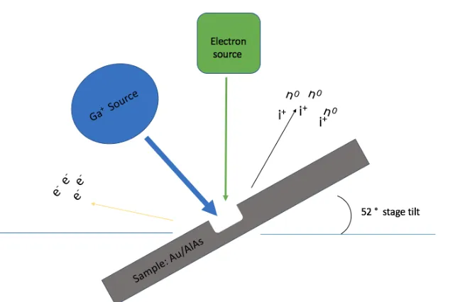
3.3 Focused Ion Beam
An effective means of etching at a high level of precision and accuracy was with the use of a focused ion beam (FIB). FIB technology has enabled the development of scanning probe tips [2] mask less FIB lithography [3] and many other advancements in the area of nanofabrication, the FIB was housed in a class 100 cleanroom in the IMDEA Nanoscience Institute in Madrid. We employed a dual FIB-SEM system, in addition to the Ga+ reservoir (beam source), an electron beam was used as a SEM to image the sample and provide accurate milling or deposition of materials with high resolution imaging. However imaging with low Ga ion beam currents (30-50pA) is feasible but at much lower resolutions and can degrade the sample, the FIB can also be used as a means of deposition.
The dual FIB-SEM beam had a working distance of 5mm, the standard FIB commonly uses a liquid metal gallium ion source due to its low melting point (~300k), low volatility, unreactive nature and its vacuum properties, additionally gallium is preferred for milling due to its weight. When the gallium is heated such that it forms a liquid metal ion source (LMIS), it is focused on a tungsten needle tip. The LMIS forms what is known as a Taylor cone due to an external electric field and the surface tension of the liquid Gallium, which occurs when the gallium is subject to an electric field. As the electrostatic field is increased field emission of the ions occurs and the ions are subsequently focused by an electrostatic lens. As the ions are directed to the surface of the sample sputtering of the sample takes place and the sputtered ions and their corresponding electrons leave the surface and are able to form an image similar to that used by an SEM. The resolution of the FIB is limited to 5nm by the mentioned sputtering process (at low powers).
[image:30.595.73.390.440.653.2]A challenge that arose in using the dual FIB-SEM was calibrating the concentric axis where both the FIB and SEM lay. The initial calibration process required that we applied a low FIB beam current to etch a visible mark on the sample to gauge where the ion beam would mill. Repositioning the stage to mill subsequent other devices requires that we repeat this step to gauge to a better degree (although still approximate) the exact location of where the milling will take place. This was often an inaccurate and time consuming method as we regularly encountered that our ion beam was a few hundred nanometres off, the results were FIB etches that would produce RTDs with isolated active regions and asymmetric cavities. Figure 3.3c highlights a case where poor alignment and inaccurate gauging resulted in a device with less laterally confined active regions than aimed.
Figure 3.3: (a) SEM image of a 3x3 μm sized mesa RTD prior milling. (b) A device post milling with FIB with four laterally confined active regions. (c) 4x4 μm sized mesa RTD with Poor alignment of ion beam stencil on the sample results in imperfect etch cavity on the mesa.
3.4 Electronic characterisation
Prior to any modification to our devices we required a full electronic characterisation, we measured current-voltage spectrums (IV curves) of our devices under both bias; before and after modification and under low temperature to observe interesting features. By applying a voltage sweep we recorded subsequent values of current, in each case we relied on a source measure unit (SMU) to source the a
c
desired input voltage and measure the output current. Regardless of our setup and our desired environment (i.e. low temperature/room temperature).
3.4.1 Source measure unit
The SMU (Keithley 2400) is an electronic instrument that can be used to both source and measure electronic components simultaneously, it allows for high precision characterisation of electronic components. We resorted to a python script written by R.Bernardo-Gavito that would source voltage and measure current, the script allowed us to vary the measurement resolution and basic sweeping parameters such as compliance and initial and final voltage values. In our setup we employed a sourced delay measurement cycle; following an applied voltage a delay time is induced to allow the source to reach the desired value (dependent on the capacitance of the internal circuitry of our RTDs) which we set to 50msbased on the previous suggestion and work by J.Roberts. Power line induced AC noise can inhibit measurement resolution however by allowing an increased AC line integration time for our measurements we can increase the resolution of our measurements; a trade-off is reduced measurement rate. We set our NPLC value to a recommended 0.05.
Figure 3.4: (a) IV characteristic of a RTD taken with a 100 step resolution. (b) IV characteristic of a RTD taken with a higher 300 step resolution showing little observable difference.
The number of steps determined how many individual points of data were plotted. 100 steps were sufficient in producing a detailed IV spectrum however in many cases we resorted to a higher resolution of 400. A fixed current compliance was kept which prevented an overload of current, the value of such varied depending on the device size as different RTD devices reached resonance at different currents (Fig 1.2).
3.4.2 Room temperature probe station
A mechanical probe station (Wentworth Lab MP2010) was used to obtain characteristic measurements of semiconducting devices. Manipulators allow precise positioning of tungsten needles to allow electrical stimulation and in many cases, can incorporate cryogenic conditions. Tungsten probes with an average radius of 1 μm, we assume negligible resistance from the probes and hence rely on a 2-terminal sensing setup. The nature of the size of samples examined with a probe station necessitates a microscope to allow for fine positioning of the probes. An advantage of the mechanical probe station is the efficiency in characterisation, given an average characterisation time of
approximately five seconds, we are potentially able to measure hundreds of devices per hour assuming parameters (i.e. compliance) remain constant. The process of repositioning the probes and sample requires little time.
[image:33.595.118.431.251.478.2]However repeated measurements on the probe station induced aggravated contact damage (Fig 3.5), such increased the likelihood of unstable readings due to discontinuities and current fluctuations. In addition to the afore mentioned issues; the probe station used was subject to vibrations from an unknown source, due to the size and weight of the probe station relocating such was infeasible. External vibrations yielded inconsistent measurements, nevertheless we in our case we found vibrations to be negligible when the sample was repositioned.
Figure 3.5: (a) IV characteristic of an RTD measured in a cryogenic probe station showing high levels of instability, potentially attributed to damaged contacts.
3.5 Micro wire bonder
contact pad. When conducted successfully the ball bonding method yields the most robust means of inter connecting semiconductor terminals.
Figure 3.6: Gold ball bonding procedure. (1) Plasma rapidly heats the end of a gold wire. (2) A ball forms due to surface tension and is positioned over the initial contact. (3) The ball bonds to the contact and the capillary is positioned over the second contact to close the loop. (4) The capillary contacts the other pad and bonds a wedge, closing the loop.
However the fabrication process is time consuming and on average only 50% of all bonds are successfully bonded. In many cases during the lift off stage, the ball tears the sample’s contact, exposing the InP substrate (Fig 3.8). There exists very little control over the dimensions of the ball and due to the nature of the positioning of the capillary and sample and control over the exact positioning of the ball, an issue arises due to the average diameter of the ball being approximately 2.1mm upon deposition. This allows very little room for error (approx. 0.3mm) and in many cases the ball comes into contact with contact B creating an unwanted secondary current path, rendering the device defective unless the contacted area is isolated or a probe station is used.
1. 2.
Figure 3.7: Dimensions of free space for ball bond. Ball bonds to contact A, wedge bonds to contact B. The red circle highlights the average maximum area a bonded ball can occupy, highlighting the average space available as 0.3mm.
Figure 3.8: (a) An array of four RTDs, two leftmost show contact pads thathave been removed during lift off stage of ball bonding, the two rightmost have been untouched. (b) The initial bond has come into contact with contact B creating an alternate current path. (c) contact damage due to tungsten probes.
3.6 Cryogenic measurements
In order to elucidate interesting features we may observe at room temperature, we comment on the interesting effects of temperature on the band structure of our RTD in chapter 2. It has been reported in the literature that at cryogenic temperatures (sub 120k) the tunnelling mechanism of certain types of heterostructures (i.e. III-Nitride tunnel diodes) becomes more prominent [6]. For this and other reasons we decided to study the RTD’s characteristic under cryogenic conditions.
3.6.1 Low temperature probe station
We initially resorted to the low temperature (LT) probe station (Lakeshore PS-100) such required the use of a vacuum chamber and cryogenic storage dewar. Prior to cooling the system, the chamber was first vacuumed and reduced to a pressure of 10-6 bar. This process ensured that moisture upon cooling does not allow ice to form and reheating does not cause the build-up of condensation. Liquid nitrogen was stored and transported via the dewar where it was injected into the vacuum chamber. Despite a temperature range of 4.2K-475k, the lowest temperature obtained was 77k due to the boiling point of nitrogen. Modulation of the temperature was possible with a heater (Lakeland 336 Temp Controller), however our preliminary cryogenic measurements did not make use of such. We experienced the same difficulties that were faced with the room temperature probe station, namely aggravated probes. Additionally we experienced a great deal of insensitivity with the micro positioners, hence experienced difficulty in positioning our probes accurately and often damaged the contacts (Fig 3.8). We resorted to bonding our samples via the method highlighted above (3.5) to avoid such.
3.6.2 Helium flow cryostat
Figure 3.9: (a) 2 point measurement with large in series resistance due to constantan wiring of the cryostat, the SMU is highlighted as a cell and ammeter sourcing voltage and measuring current. (b) Standard 4-point measurement, two terminals measuring the potential difference across our RTD (Vm), and two sourcing voltage (vs), measuring current (Im).
We’ve outline a range of methods that we employed in our study. They range from methods of characterisation to modification and we have briefly commented on the difficulties and sources of error in our methods. We note the difficulty faced when studying our sample under cryogenic conditions and when preparing our RTDs with the micro wire bonder as well as how effective apparatus such as the SMU/probe station were. In the forthcoming chapter we pay close attention to our results and assess how effective our methods were.
Bibliography
[1] A. R. Clarke, Microscopy techniques for materials science., CRC Press (electronic
resource), 2002.
[2] e. a. J.R. Krogmeier, Focused ion beam modification of atomic force microscopy tips for
near-field scanning optical microscopy, vol. 79, Appl. Phys. Lett., 2001.
[3] J. Melngailis, Focused, ion beam lithography, vol. B80/81, Nuclear Instr. and Meth. in
Phys. Res., 2993, p. 1271.
[4] A. e. c. a. packaging., “"Gold Bonding Wire and Ribbon: Wire for Automatic Bonders",”
2014. [Online]. Available:
http://www.ametek-ecp.com/products/componentswire/wireandribbon/goldwireandribbon. [Accessed
2017].
[5] V. V. e. al., “Design and experimental evaluation of compensated bondwire
interconnects above 100 GHz,”
International journal of Microwave and Wireless
Technologies. ,
vol. 7, no. 3-4, pp. 261-270, 2015.
Chapter 4- Experimental Results
4.1 Introduction
In the previous chapter we have described the methods used to obtain our results. We now present in this chapter the combination of the methods introduced in chapter 3 with the hypothesis established in chapter 2 to increase the bit density of the QCPUF such that our UO (unique object) has an increased level of complexity. We used a FIB (focused ion beam) to introduce multiple areas of confinement (by laterally restricting areas) within the heterostructure. We present our results through the characterisation of our RTDs in different conditions and observed a number of features that are of interest. Our results bare close resemblance to the results of previous work carried out by Reed et al. We compare and contrast such results however as a solution to the bit density problem of the QCPUF further investigation is required.
4.2 Increased Bit Density
4.2.1 Introduction
In the area of forensics the familiar fingerprint which is used in identification relies on the complex structure and random pattern of its own minutia. There exist over eight different types of minutia that range from the small ridges and islands to the complex bifurcations on one’s fingerprint. In a nutshell, an algorithm converts the unique pattern derived from the combination of different minutia to generate a unique identity that is then the basis for identification and security.
Previous work on QCPUF’s using RTDs only rely on the peak position as the only minutia and hence source of true uniqueness. To realise the full potential of a ‘quantum fingerprint’; the need to incorporate further minutia will undoubtedly bring the QCPUF closer to a fingerprint like architecture. It has been proposed in the literature [1] that in addition to the peak position one can utilise the valley, peak to valley ratio (PVR) and tunnelling region to use as the UO.
We explored up to 8 different etch designs over 69 devices however our most recurring results were characterised as: 1) second resonance peak and 2) bumps within NDR region. Prior to modifying our devices with the FIB, we recorded the IV characteristic in the negative bias (axis inverted), however at times we observed interesting features in both biases, as a comparison metric we were only able to compare our before and after sweeps in the negative bias. In many cases we present only the IV characteristic under the negative bias, as generally broader peaks and larger PVR are observed under such bias. We also produced a set of devices whose final surface area was less than 4 μm2 (the current minimum of such RTDs) with a clear NDR region resulting in an increase in bit density per unit volume.
4.2.2 Etch designs and parameters
We began with 195 devices on our chip, 133 of these devices were functioning and were considered suitable for modification by the FIB. We modified 69 with the FIB and out of these approximately 30 were functioning post modification. Overall we proposed eight etch designs in an attempt to successfully introduce more confined states. We observed that some designs were more successful than others and the overview of the designs can be summarised in Table 4.1 below.
However it is important to note that in these measurements we did not consider parameters that would affect etch rate from the FIB; i.e. the intensity of the Gallium ion beam, etc. such are discussed further in chapter 5.
[image:40.595.78.515.290.521.2]4.2.3 Lateral etch
We began our investigation with lateral etches gradually decreasing the area of the device such that we aim to identify the cross-over from 2D to 1D confinement. Our goal was to explore the potential of confining our electrons to a further two dimensions such that we create a 1D structure (quantum wire). Unfortunately, the majority of our results were unsuccessful in showing clear signs of increased confinement and many of which were defective post FIB. However some modified devices did yield interesting results. It is important to note that some lateral etches were solely for testing preliminary FIB parameters and resulted in significantly damaged devices. Devices whose IV characteristic did not present a clear NDR, were characterised as defective devices and exhibited high instabilities, high in parallel/in series resistance and at times showed open/short circuits . Our devices’ initial surface area ranged from 4 μm2 to 25 μm2 sized mesas. We explored a wide variety of dimensions that ranged from reducing our structure by a factor of two to a factor of four (Fig 4.1). Overall our device areas ranged from 2 μm2 to 13 μm2.
,
Figure 4.1: SEM image of device B4 (left) showing a lateral etch that has thus reduced the active area by half. A9 (right) post FIB RTD, with a minimal active region marked by A.
Out of the nineteen devices modified, six were functioning post-FIB (Table 4.2). We attribute such a low success rate to the intensity of the Ga ion beam which can affect the doping profile of the layers, however as we etched more structures we altered the intensity of the beam and milling duration to aggravate the active regions much less.
A primary feature we observed with all functioning devices post FIB was a decrease in both current and voltage resonance value. We attribute this to the reduced size of the device and to the proportionality of current density. Where the current density (J) is a measure of the electric current (I) per unit area of cross section (A); J=I/A, assuming that the motion of current is orthogonal to the surface A.
A
We observe multiple interesting factors post FIB for device B7 (Fig 4.2). Dissecting our IV characteristic into distinctive regions; beginning with the tunnelling region. By mere observation we can see a decreased stability in the tunnelling region which may be attributed to defects induced by the FIB, an undesirable feature we wish to avoid. We observe a decreased resonance peak current and observe a secondary peak at 0.48V.
Table 4.2: Devices etched laterally, showing their initial and final peak and valley positions and their corresponding initial (PVRi) and final (PVRf) peak to valley ratio. In all cases we observe a decrease in PVR (as low as 1.15).
Figure 4.2: IV characteristic of device B7 before and after treatment with FIB, where a visible secondary peak and corresponding NDR is visible post modification (red). Minimal in series and in parallel resistance is observed.
working device (2.25 μm2 ) operating at 25% lower power. As A9 was our smallest functioning device we have ultimately increased the bit density by a factor of 4.2 (Fig 4.3).
Figure 4.3: IV characteristic of A9 before and after being treated with a FIB showing instability in the NDR and increase in parallel resistance causing a shift in peak current. The before IV characteristic shows a more defined resonance peak and stable PDR.
4.2.4-Dimond etch
[image:43.595.67.463.110.369.2]Following our improved etch parameters we employed a design that yielded a 60% success rate. The aim of the diamond etch was to induce maximum probability of confinement within the corners of the cavity (Fig 4.4). Our devices’ initial surface area ranged from 4 μm2 to 36 μm2 sized mesas, with a maximum confinement post FIB of up to 55nm (Table 4.3).
Table 4.3: Devices etched with a diamond cavity, showing their initial and final (post FIB) peak and valley positions and their corresponding peak to valley ratio (PVR). We observe two devices with final surfaces areas of less than 4 μm2.
Out of the three functioning devices (E1, D11, A11) we observed two devices (D11 & A11) in particular that not only gave relatively stable and repeatable IV characteristics but also a hint of secondary resonance peak. The third device (E1); although functioning exhibited high instabilities, we were unable to observe a consistent and repeatable resonance peak, although we are able to extract an average peak and valley position, we characterise such a device as unstable (Fig 4.5).
What is interesting to note with D11 and A11 is the existence of a second resonance peak post modification. There exists in both cases after the resonance peak and for both devices of identical size prior modification and near identical post modification sizes, the second peak exists at similar locations with an offset of (± 0.01V, ± 0.002mA). A phenomena we initially attributed to increased confinement.
![Figure 1.1b: A flake of WS2 showing a PL map of peak wavelength [8].](https://thumb-us.123doks.com/thumbv2/123dok_us/9382040.441207/10.595.149.412.86.339/figure-flake-ws-showing-pl-map-peak-wavelength.webp)

![Figure 2.10: Variation of bandgap of GaAs with temperature showing an increase in bandgap as temperature decreases [16]](https://thumb-us.123doks.com/thumbv2/123dok_us/9382040.441207/27.595.146.394.77.310/figure-variation-bandgap-temperature-showing-increase-temperature-decreases.webp)