Self-Assembled Arrays of Magnetic
Nanostructures on Morphologically
Patterned Semiconductor Substrates
by
Brendan O’Dowd
A thesis submitted to the University of Dublin in partial fulfilment for the degree of Doctor of Philosophy
School of Physics Trinity College Dublin
University of Dublin Dublin 2
Ireland
Declaration of Authorship
This thesis is submitted by the undersigned for examination for the degree of Doctor of Philosophy at the University of Dublin. It has not been submitted as an exercise for a degree at any other University.
With the exception of the assistance noted in the acknowledgements, this thesis is en-tirely my own work.
I agree that the library of the University of Dublin may lend or copy this thesis freely upon request.
Signed:
Date:
Summary
This thesis deals with the formation of morphological patterns on single-crystal semi-conductor surfaces via self-assembly processes, followed by the subsequent fabrication of magnetic nanostructures whose dimensions are defined by the underlying template. Stepped surfaces on Si (111) were achieved by high temperature DC annealing of vici-nal Si templates which causes the atomic steps to form step-bunches and/or facets. In particular, for templates annealed with the current directed in the ascending step di-rection it was shown that the cooling rate from the annealing temperature can be used as a precise control of step periodicity. A shallow angle deposition technique was used to create ordered rows of magnetic nanowires on the step-bunched Si templates, whose dimensions are determined by the size of the underlying steps as well as the duration and angle of deposition. It is shown that wire width can be well defined down to as low as 30 nm and that the technique is applicable to a range of magnetic materials. Ordered arrays of nanodots can also be grown via shallow angle deposition onto faceted vicinal alumina templates, and it is shown that the substrate temperature during deposition influences the ellipticity and separation of the nanodots produced.
Magnetic measurements reveal that the nanowires have in-plane magnetic shape anisotropy, while measurements of coercivity as a function of temperature allow the investigation of parameters relating to the energy barriers of magnetisation reversal. Henkel analysis was used to probe the extent of interwire interactions, and it was shown that reducing interwire separation led to dipolar coupling, as had been shown in previous studies of vertical wire arrays. The samples were also investigated using FMR, with measurements being taken as the sample was rotated about each of its principal axes. The results of this study indicated that the use of MgO as a capping layer leads to the formation of an oxide layer which may reduce the effective thickness of the nanowires, and over time gives rise to an additional unidirectional exchange anisotropy. Some preliminary results obtained through the analysis of first order reversal curves (FORCs) are also presented. This method of analysis has the potential to identify the influence of one-dimensional structures as well as superparamagnetic nanoparticles on the magnetisation of the sys-tem as a whole, and it is likely to be a very useful tool for future investigations into the properties of such magnetic nanostructure arrays.
particles (gold nanodots) are defined using EBL, resulting in far greater wire uniformity and thereby facilitating comparisons between different growth conditions. For example, the effects of shadowing as a function of separation between neighbours in the array can be quantitatively measured, and a simple model is presented which closely matches the experimental data. The study of GaAs nanowire growth from pre-patterned seed particles is also important from an applications point of view, since most proposed ap-plications require the precise placement of nanowires rather than arbitrary locations. Growth in As-limited conditions was investigated, a regime which is usually ignored in studies of nanowire growth that uses catalyst particles. Many features of previous studies were replicated, but at a significantly lower growth temperature allowed through the use of Au catalyst particles. Growth under As2 flux was compared to As4. There were prominent differences in shape, volume and facets making up the wire sidewalls. These findings were related to the different reactivities and diffusion properties of the two molecules on the nanowire sidewalls.
The control of shadowing allowed substantial radial growth to occur uniformly along the wire sidewalls. This effect resulted in wires which were much wider than the seed particles (for example wires with diameter of ≈300 nm width having droplet diameters of only 20 nm was common). In all instances, the radial growth occurred epitaxially, with no defect planes in the axial direction seen in any sample. Some samples had a certain density of wurtzite to zincblende defects or zincblende twinning planes. These defects traversed the wire width in each case. Moreover, the appearance of these defects was closely associated with instances where the contact angle between the nanowire sidewalls and the alloy droplet atop the wire was significantly greater or less than 90◦. This phenomenon is described in detail in relation to the crystal structure at the growth interface.
Acknowledgements
Throughout the past four years I have had the great fortune of meeting and working with some wonderful people. I would like to thank all those who were so generous with their time. They really have been an inspiration for me.
I would like to thank my supervisor Prof. Igor Shvets for all of his support and guidance. In all my dealings with Igor I have always found him to be very easy to work with. He has always been a good listener and very thoughtful in his approach.
I would like to thank everyone in the Applied Physics Research Group for their support, advice and good humour. Their attitude has made coming to work every day for the last four years a very positive experience, and I have always appreciated the lengths that they have all gone to whenever I needed help. Ruggero has been a great friend and a valuable source of advice. Cormac has been very helpful with his guidance, particularly in practical lab matters. Sunil contributed to planning and trained me on range of equipment. Karsten has been very generous, regularly putting aside his work to help me for as long as was needed. Ciar´an has been a great help with administrative issues and has saved me countless headaches. In the run-up to submission, Barry and Ellen were both invaluable sources of support and advice.
I have greatly enjoyed working at CRANN and in the School of Physics. In both in-stitutions there is a wealth of experience and advice. I’d like to thank all the staff and researchers here who contribute to the wonderful working environment.
I’d like to thank Prof. Jacek Furdyna for welcoming me into his group. He has a passion for research that is contagious and a very warm personality that made working with him a pleasure. I’d like to thank the other professors in the group; Xinyu Liu, Malgorzata Dobrowolska, and Tomasz Wojtowicz. Prof. Liu and Prof. Wojtowicz put in a great deal of work in the fabrication of samples for my analysis. I’d like to thank Brendan Benapfl, Joe Hagmann, Jon Leiner and Rich Pimpinella for making sure that I now have great memories as well as some good data from my time at Notre Dame. I had a great time getting to know each of them. I worked closely with Dr. Sergei Rouvimov who took some excellent TEM images. I’d like to thank Sergei for his kind attitude and acknowledge his talent and hard work. In general I had a great time at Notre Dame. There was a very positive and calm atmosphere and it was a great place to work. I’d like to thank all the other Ph.D. students there as well as the staff at the Department of Physics, especially Susan and Shari who were very welcoming and helpful.
I would also like to acknowledge the input of all of our collaborators. Pardeep Thakur and Nicholas Brookes conducted XMCD measurements for us at the European Synchrotron
Radiation Facility. Sarnjeet Dhesi carried out some XMCD measurements at the Dia-mond Light Source in Oxfordshire, England. Some TEM images of our nanowire arrays were taken by the Atomic Manipulation Spectroscopy Group at the Catalan Institute of Nanotechnology. Kritsanu Tivakornsasithorn and Richard Pimpinella participated in the FMR and SEM investigations of the Fe-coated GaAs nanowires. FMR measurements and analysis were carried out by the group of Oleksandr Tovstolytkin at the Institute of Magnetism in the National Academy of Science of Ukraine, in Kiev, Ukraine. EBL for the patterned arrays of Au nanodots which formed the seed particles for the GaAs nanowire arrays was carried out by the Growth and Physics of Low Dimensional Crystals group under Prof. Wojtowicz at the Institute of Physics, Polish Academy of Sciences, Warsaw, Poland. I should also mention here that some software was used which was free to download, namely Gwyddion which was used for AFM analysis and generating FFTs in post-production, and FORCinel for Igor Pro, which which was used to process the FORC data.
I would like to thank Zara for her love and support throughout my studies. She has been great in every way and is always there for me through all the ups and downs. Thanks to all my close friends over the past few years. Thanks to my teachers and lecturers through the years. Thanks to my brothers Ciar´an, Enda and Patrick, and a huge thanks to my parents for all the sacrifices they made for my education.
Contents
Declaration of Authorship iii
Summary v
Acknowledgements vii
List of Figures xiii
List of Tables xvii
Abbreviations xix
Publications xxi
1 Introduction and Motivation 1
1.1 Manipulation of Semiconductor Surfaces . . . 1
1.2 Magnetic Nanostructures . . . 3
1.3 Thesis Outline . . . 6
2 Experimental Methods 9 2.1 Sample Fabrication . . . 9
2.1.1 Vacuum System for Si Annealing and Glancing Angle Depositions . . . 9
2.1.2 GaAs Nanowire Growth Chamber . . . 12
2.1.3 Tube Furnace . . . 13
2.2 Characterisation of Sample Morphology . . . 13
2.2.1 Atomic Force Microscopy (AFM) . . . 13
2.2.2 Scanning Electron Microscopy (SEM) . . . 14
2.2.2.1 Additional SEM capabilities . . . 17
2.2.3 Transmission Electron Microscopy (TEM) . . . 18
2.2.4 Scanning Transmission Electron Microscopy (TEM) . . . 19
2.2.5 Statistical Analysis of Nanoparticle Dimensions . . . 19
2.3 Magnetic Characterisation . . . 20
2.3.1 Vibrating Sample Magnetometer (VSM) . . . 20
Contents x
2.3.2 Alternating Gradient Field Magnetometer . . . 21
2.3.2.1 Addition AGFM Measurements . . . 21
2.3.3 Ferromagnetic Resonance (FMR) . . . 23
3 Template Preparation and Glancing Angle Deposition 27 3.1 Background . . . 27
3.2 Si Template Preparation . . . 30
3.2.1 Si (111) . . . 30
3.2.2 Step Bunching on Si (111) . . . 33
3.2.2.1 BCF and Stoyanov Theory . . . 36
3.2.2.2 Faceting in Regime I . . . 38
3.2.3 Si Annealing Procedure . . . 39
3.2.4 Results . . . 41
3.3 Sapphire Template Preparation . . . 45
3.3.1 Sapphire . . . 45
3.3.2 Faceting Mechanism on Sapphire . . . 45
3.3.3 Annealing Procedure . . . 48
3.3.4 Results . . . 48
3.4 Glancing Angle Deposition Technique . . . 49
3.4.1 Nanowires Grown on Large-Step Samples . . . 51
3.4.2 Nanowires Grown on Small-Step Samples . . . 51
3.4.2.1 Downhill Depositions on Si . . . 51
3.4.2.2 Uphill Depositions on Si . . . 57
3.4.2.3 Uphill Depositions on Sapphire . . . 59
3.5 Conclusions . . . 61
4 Magnetic Characterisation of Nanowire Arrays 63 4.1 Magnetic Phenomena in Nanowire Arrays . . . 63
4.1.1 Magnetic Anisotropy . . . 64
4.1.1.1 FMR as a probe of magnetic anisotropy . . . 68
4.1.2 Important Length Scales in Magnetism . . . 69
4.1.3 Reversal Mechanisms . . . 71
4.1.4 Interwire Interactions . . . 73
4.2 Results . . . 75
4.2.1 Shape Anisotropy . . . 75
4.2.2 Reversal Mechanism . . . 79
4.2.3 Interwire Interactions . . . 82
4.2.4 FMR . . . 84
4.3 Conclusions and Further Work . . . 91
5 GaAs Nanowires 99 5.1 GaAs . . . 99
5.2 Motivation for Ordered Arrays of GaAs nanowires . . . 99
5.3 VLS Method . . . 100
5.4 Crystal Structure of GaAs Nanowires Grown in [111] Direction . . . 106
5.5 GaAs Nanowire Fabrication Procedure . . . 112
Contents xi
5.6.1 Ordered Arrays of Nanowires . . . 114
5.6.2 Pencil-Shaped Nanowires . . . 117
5.6.3 Examination of Effect of Shadowing for Pencil-Shaped Nanowires . 120 5.6.4 Critical Dot Diameter for Nanowire Growth . . . 123
5.6.5 Growth in As-limited Regime . . . 126
5.6.6 Nanowire Growth using As Dimers . . . 136
5.7 Conclusions and Further Work . . . 144
6 GaAs Nanowires Coated with Fe 147 6.1 Introduction . . . 147
6.2 Experimental Procedure . . . 149
6.3 Results . . . 150
6.3.1 SEM . . . 150
6.3.2 STEM and EDX . . . 151
6.3.3 FMR . . . 153
6.4 Conclusions and Further Work . . . 155
7 Conclusions and Outlook 157
A Derivation of Magnetic Resonance Expression 163
B Effect of Shadowing on Nanowire Volume 169
List of Figures
1.1 Typical FED design incorporating nanowire array . . . 3
1.2 HDD units from 1956 and 2008 . . . 4
2.1 Chamber for glancing angle deposition and Si annealing . . . 10
2.2 Glancing angle deposition schematic . . . 11
2.3 VLS Chamber . . . 12
2.4 SEM Schematic . . . 15
2.5 SEM Interaction Volume . . . 16
2.6 Statistical Analysis using AutoCAD . . . 20
2.7 Schematic for finding MR(H) andMD(H). . . 22
2.8 Schematic for finding FORCs. . . 23
2.9 FMR Setup Schematic . . . 24
3.1 Unit cell of Si. . . 30
3.2 Atomic steps on Si(001) . . . 31
3.3 The (111) surface of Si . . . 31
3.4 Single atomic steps on Si (111) . . . 32
3.5 Si 7×7 reconstructed surface unit cell . . . 33
3.6 Cubic model of atom locations . . . 35
3.7 Schematic of adatom gradient effect on terrace of atomic step . . . 37
3.8 Two Si (111) terraces separated by a (331) facet . . . 39
3.9 Samples annealed with step-up current in Regime I with different cooling rates . . . 41
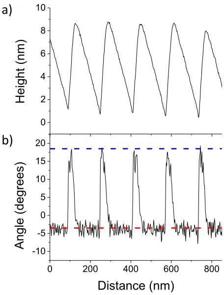
3.10 Dependence of periodicity on cooling rate for step-up current in Regime I 42 3.11 Height and angle profile of a step-bunched sample . . . 43
3.12 Step bunches in Regime I and II . . . 44
3.13 Crystal structure of Al2O3 . . . 46
3.14 Side profile and C-plane of Al2O3 . . . 46
3.15 Dependence of periodicity of annealed Al2O3 substrates on temperature . 47 3.16 AFM of faceted Al2O3 . . . 49
3.17 Glancing Angle Deposition Schematic . . . 50
3.18 Glancing angle deposition results on large-step samples . . . 52
3.19 Single nanowire produced on a large-step sample . . . 52
3.20 Fe nanowires with varying deposition angle . . . 53
3.21 Height profiles across nanowires with varying deposition angle and thickness 54 3.22 TEM of Fe nanowires . . . 55
3.23 TEM of Co nanowires . . . 56
3.24 AFM data from Ni nanowire arrays with varying thickness . . . 57
List of Figures xiv
3.25 AFM data from arrays of nanowires composed of Co, Fe and Ni deposited
in the uphill direction . . . 58
3.26 Co nanowires and nanoparticles on faceted Al2O3 substrates . . . 59
3.27 Important dimensions of Co nanoparticles . . . 60
4.1 Labels and axes of wire array parameters. . . 68
4.2 Schematic images of the effect of dipolar coupling with nanowire arrays. . 74
4.3 Shape Anisotropy of Fe nanowire arrays of varying thickness. . . 76
4.4 Dependency of wire structure on deposition thickness. . . 77
4.5 Shape Anisotropy of Co nanowire arrays of varying thickness. . . 78
4.6 Dependency of coercivity of Fe nanowire arrays as a function of temperature 80 4.7 SEM images of samples for Henkel analysis. . . 82
4.8 M−H loops for samples in Henkel analysis. . . 83
4.9 Henkel plots for varying separation. . . 84
4.10 Axis and angle labels for FMR. . . 85
4.11 In-plane FMR spectra for Fe nanowire array. . . 86
4.12 Out of plane FMR spectra for Fe nanowire array. . . 87
4.13 Sample of FMR spectra. . . 88
4.14 Resonance Field as a function of angle. . . 89
4.15 Resonance Field as a function of angle for sample with ageing effects. . . . 90
4.16 Signatures of magnetic features on a FORC distribution plot. . . 94
4.17 FORC plot for Fe nanowire array. . . 95
4.18 FORC distribution plots for different nanowire and nanodot arrays. . . 96
5.1 Routes of Ga to growth interface . . . 103
5.2 Unit cell of zincblende GaAs. . . 107
5.3 Different Hexagonal Facet Groups for Zincblende and Wurtzite Structures. 109 5.4 Schematic of contact angle and angle of inclination of sidewalls. . . 110
5.5 Schematic of competing facet groups during growth. . . 111
5.6 Two possible facets of wurtzite GaAs nanowire sidewalls. . . 112
5.7 Liquid-solid phase boundaries for AuGa and PdGa alloys. . . 113
5.8 Ordered and Random Array of GaAs Nanowires. . . 114
5.9 Height Distributions for Ordered and Random Nanowire Arrays. . . 115
5.10 TEM analysis of wires in patterned array. . . 116
5.11 SEM images of pencil-shaped nanowire array. . . 117
5.12 TEM images of pencil-shaped nanowire. . . 119
5.13 Dependency of Nanowire Volume with Separation. . . 121
5.14 Dependency of nanowire volume distribution with separation. . . 122
5.15 Nanowire volume vs. separation with numerical model . . . 123
5.16 Probability of Nanodot initiating Wire Growth vs. Radius of Nanodot. . . 125
5.17 Nanowires grown in As-limited regime . . . 127
5.18 Histogram of heights of nanowires grown in As-limited regime . . . 127
5.19 Nanowires grown from patterned arrays in As-limited regime . . . 129
5.20 STEM of Nanowires grown in As-limited regime . . . 130
5.21 EDX examination of Nanowires grown in As-limited regime . . . 131
List of Figures xv
5.23 High resolution TEM images taken of a nanowire grown in As-limited
conditions. . . 133
5.24 Schematic of nanowire with microfacets . . . 134
5.25 As-limited growth of shorter duration . . . 134
5.26 Nanowires grown using As2 . . . 137
5.27 Volume of cone-shaped nanowires as a function of separation . . . 138
5.28 2D density plot of wire heights and angles . . . 139
5.29 2D density plots of wire heights and angles for wires with varying droplet diameter . . . 140
5.30 TEM analysis of wire with small droplet grown in As2. . . 141
5.31 TEM analysis of wire with large droplet grown in As2. . . 142
5.32 Contact angles for wires with varying droplet size . . . 143
6.1 Growth directions of GaAs nanowires on various GaAs substrates . . . 149
6.2 GaAs Nanowire arrays coated in Fe and Au . . . 150
6.3 STEM and EDX linescans of Fe/Au coated GaAs nanowires . . . 151
6.4 STEM and EDX linescans of particular features on Fe/Au coated GaAs nanowires . . . 153
6.5 FMR of Fe-coated GaAs nanowires . . . 154
A.1 Spherical co-ordinate system used in FMR . . . 163
A.2 Labels and axes of wire array parameters. . . 166
B.1 Schematic of shadowing considerations . . . 170
B.2 Effect of varying values for the diffusion length (D) . . . 172
B.3 Effect of varying the initial nanowire diameter . . . 173
List of Tables
3.1 Si (111) Step-Bunching Temperature Regimes . . . 34
3.2 Average dimensions of nanoparticles grown at two different substrate de-position temperatures . . . 60
4.1 Demagnetising Factors for Common Shapes . . . 67
4.2 Useful parameters for common ferromagnetic materials . . . 71
4.3 Fitting parameters of temperature dependence of coercivity . . . 80
4.4 Summary of Fe nanowire array samples analysed with FMR. . . 87 4.5 Parameters determined from fitting to samples with unidirectional anisotropy. 91
Abbreviations
AAO Anodized Aluminium Oxide
AFM Atomic ForceMicroscope
AGFM Alternating Gradient Field Magnetometer
ATLAS Atomic TerraceLowAngle Shadowing
BSE Back-Scattered Electrons
CBE ChemicalBeam Epitaxy
DMA DifferentialMobility Analyser
EBL ElectronBeamLithography
EDX EnergyDispersiveX-ray Spectroscopy (Sometimes also referred to as EDS or XEDS)
FED Field Emission Display
FMR FerromagneticResonance
GMR GiantMagnetoresistance
FFT Fast Fourier Transform
HAADF High-Angle Annular Dark Field (Imaging)
HDD HardDiskDrive
LCG Laser-AssistedCatalytic Growth
LED LightEmitting Diode
MBE MolecularBeam Epitaxy
MCD MagneticCircular Dichroism
MFM MagneticForce Microscopy
MOVPE Metal OrganicVapour Phase Epitaxy
OAG OxideAssistedGrowth
PE Primary Electrons
PEM PhotoElastic Modulator
Abbreviations xx
PPMS Physical Properties Measurement System
SAED SelectiveAreaElectronDiffraction
SAG SelectiveAreaGrowth
SE Secondary Electrons
SEM Scanning Electron Microscope
(S)MOKE (Surface)Magneto Optic Kerr Effect
STEM Scanning TransmisisonElectronMicroscope
STM Scanning Tunnelling Microscope
TEM Scanning Electron Microscope
UHV UltraHigh Vacuum
VLS Vapour LiquidSolid
VSM Vibrating SampleMagnetometer
XAS X-ray AbsorptionSpectroscopy
XMCD X-ray Magnetic Circular Dichroism
Publications
Arora, S. K., ODowd, B. J., McElligot, P. C., Shvets, I. V., Thakur, P., and Brookes, N. B. (2011). Magnetic properties of planar arrays of Fe-nanowires grown on oxi-dized vicinal silicon (111) templates. Journal of Applied Physics, 109(7), 07B106. doi:10.1063/1.3554264
Arora, S. K., ODowd, B. J., Ballesteros, B., Gambardella, P., and Shvets, I. V. (2012). Magnetic properties of planar nanowire arrays of Co fabricated on oxidized step-bunched silicon templates. Nanotechnology, 23(23), 235702. doi:10.1088/0957-4484/23/23/235702
Fox, D., Verre, R., ODowd, B. J., Arora, S. K., Faulkner, C. C., Shvets, I. V., and Zhang, H. (2012). Investigation of coupled cobaltsilver nanoparticle system by plan view TEM. Progress in Natural Science: Materials International, 22(3), 186192.
doi:10.1016/j.pnsc.2012.04.001
Arora, S. K., ODowd, B. J., Nistor, C., Balashov, T., Ballesteros, B., Lodi Rizzini, a., Shvets, I. V. (2012). Structural and magnetic properties of planar nanowire arrays of Co grown on oxidized vicinal silicon (111) templates. Journal of Applied Physics, 111(7), 07E342. doi:10.1063/1.3679033
Pimpinella, R. E., Zhang, D., McCartney, M. R., Smith, D. J., Krycka, K. L., Kirby, B. J., Furdyna, J. K. (2013). Magnetic properties of GaAs/Fe core/shell nanowires. Journal of Applied Physics, 113(17), 17B520. doi:10.1063/1.4799252
Arora, S. K., ODowd, B. J., Polishchuk, D. M., Tovstolytkin, A. I., Thakur, P., Brookes, N. B., Shvets, I. V. (2013). Observation of out-of-plane unidirectional anisotropy in MgO-capped planar nanowire arrays of Fe. Journal of Applied Physics, 114(13), 1339031339037. doi:10.1063/1.4823514
For Zara and my parents
Chapter 1
Introduction and Motivation
This thesis deals with ordered arrays of magnetic nanowires and nanoparticles that have been deposited onto specially prepared crystalline substrates, namely the semiconductors Si and GaAs as well as the insulator Al2O3. The nanowires/nanoparticles take their shape from the texture of the substrate. As such, the two central themes of this thesis are the manipulation of semiconductor surfaces to produce ordered morphologies, and the subsequent fabrication and analysis of magnetic nanostructures.
1.1
Manipulation of Semiconductor Surfaces
The control and preparation of highly uniform single crystal structures such as Si has been a key enabler of many of the advancements that underpin the technological rev-olution of the past 50 years. While the first solid-state transistors were made using germanium, today Si is the most commonly used material for the integrated circuits which today are found in almost all electronic equipment, such as computers, radios, calculators and many more besides. Si also has important applications in the solar cell industry and a wide variety of sensing apparatus. Silicon’s popularity is also related to its abundance, being the second most common element making up the earth’s crust (after oxygen) [1]. GaAs, while not as ubiquitous as Si, has important niche applica-tions where it out-performs Si. For example, its higher electron mobility makes it a suitable candidate for the manufacture of high-frequency transistors in communications electronics.
Central to the realisation of proposed devices, and the improvement of existing ones, has been our growing awareness and ability to manipulate behaviour at the atomic level. For this reason, a huge volume of research continues to be conducted to enhance our
Chapter 1. Introduction and Motivation 2
fundamental understanding of these materials. In this work, separate investigations are carried out into particular nanoscale growth processes of Si and GaAs, which are utilised here for the subsequent fabrication of magnetic nanostructures, but are interesting in their own right as they further our understanding of the properties of these two important materials. With regard to Si, an investigation into the migration of surface atoms leading to the bunching of atomic steps is carried out as described in the first half of chapter 3. The desire to investigate and control the behaviour of atomic steps on single crystal structures is a natural outcome of the inevitability of their appearance, since, in spite of the enormous advances in crystal preparation, for device-sized pieces of Si (>µm) it is practically impossible to produce atomically flat surfaces. The long-term goals of such experiments are to learn about how these surface defects can be managed in such a way as to prevent them from influencing the proper functioning of devices, or perhaps even to open up new possibilities for functions based on the controlled use of such defects. The formation of nanowires and nanoparticles on step-bunched substrates which is described in the second half of chapter 3 can be considered a very primitive example of the latter.
Chapter 1. Introduction and Motivation 3
Nanowires
Substrate (Cathode)
Gate Material Coloured phosphors Support
matrix
Glass Transparent conducting oxide
This is a design of a field-emission display (FED) I drew in AutoCAD. It is an amalgamation of several designs I saw in different papers on FEDs. I have been deliberately vague with the design since it is only supposed to represent a possible application of a nanowire array
Figure 1.1: Typical FED design incorporating nanowire array
Possible FED (Field Emission Display) device based on an ordered array of nanowires. This design consists of an amalgamation of features typically seen in proposed FED devices [8–10].
The challenges associated with the implementation of these applications include our understanding and control of the growth process. Specifically, we would like to be able to minimise defects in the crystal structure, and specify the overall shape of the nanowire. Many proposed applications also require precise placement of the nanowires, rather than simply a disordered array. The experiments in chapter 5 regularly refer to these obstacles.
1.2
Magnetic Nanostructures
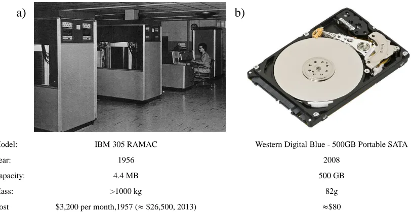
The study and understanding of magnetic nanostructures is crucial for a number of applications and their continued development, in particular for the manufacture of mag-netic data storage devices. Despite a recent slump in the hard disk drive (HDD) market due to the popularity of smartphones and tablet computers (which use flash memory), over 550 million hard disk drive (HDD) units are expected to be sold in 2013, with global sales of of approximately $33 billion [11]. The growing trend of online or ‘cloud’ storage is expected to strengthen HDD sales in the coming years.
Chapter 1. Introduction and Motivation 4
a)
b)
Model: IBM 305 RAMAC Western Digital Blue - 500GB Portable SATA
Year: 1956 2008
Capacity: 4.4 MB 500 GB
Mass: >1000 kg 82g
[image:28.596.80.487.84.294.2]Cost $3,200 per month,1957 (≈ $26,500, 2013) ≈$80
Figure 1.2: HDD units from 1956 and 2008
a) Two IBM 305 RAMAC HDDs (foreground) with operator, processing unit and console in the background. This photo is in the public domain and was taken by the U.S. Army Red River Arsenal.
b) Modern 2.5” laptop hard drive, produced by Western Digital. The photo is in the public domain. It was obtained from Wikimedia where it was uploaded by user ‘Evan-Amos’ as a part of Vanamo Media.
approximately equivalent to $26,500 in 2013 after adjusting for inflation 1[14]. It could store only 4.4-5 MB of data. Figure 1.2(b) shows a modern 2.5” laptop hard drive, which stores 500 GB and weighs less than 100 g. In terms of cost per MB, these two examples represent a decrease of over 8 orders of magnitude. The continued improvement in HDD performance and memory density are some of the main motivations behind many of the hot topics in magnetism research today. Two examples of areas of particular interest are Heat-Assisted Magnetic Recording (HAMR), which uses a laser or other localised heat source to temporarily lower the magnetisation reversal barrier of the bit being written, and Bit-Patterned Media (BPM), which uses distinct, patterned bit entities [15]. BPM has the potential for greater bit density than current designs employing granular films, though implementation of BPM will require a high throughput nanoscale writing tech-nique that is also low in cost [16, 17]. One example of a techtech-nique hoped to allow the definition of theses individual bits is nano-imprint lithography, though further improve-ments in efficiency and reproducibility are still required [18, 19]. The research in this thesis is fundamental in nature, and is not specific to any particular device design.
Another potential application for magnetic nanowires is domain wall logic [20, 21]. In such devices, Boolean logic functions such as AND, OR, NAND, XOR etc. can be carried
1
Chapter 1. Introduction and Motivation 5
out by propagating a domain wall through a specially designed circuit of magnetic nanowires, which are usually composed of permalloy (Ni80Fe20). The magnetisation will preferentially lie along one or other direction of the wires involved, corresponding to a logical 1 or 0. The initial magnetic ‘inputs’ and the propagation of domain walls are governed via the application of external fields, and the logical outcome at the output wire is determined by the manner in which the ‘input’ magnetisations interact with the circuit and each other. Prior to fabrication and testing in the lab, circuit designs are usually rigorously tested using a micromagnetic simulation software package such as OOMMF (Object Oriented MicroMagnetic Framework, ITL/NIST).
Other varied uses for magnetic nanowires include the growing area of spin transfer and spintronics [22], high frequency devices [23], magnetic sensing [24] and cell manipulation in biological systems [25].
Prior to implementation in proposed applications, a comprehensive understanding of the fundamental behaviour of the magnetisation within the wires will be required. The sensitivities of conventional magnetometers coupled with the tiny volumes of magnetic material in these structures is such that it is far more convenient to measure many thou-sands or millions of wires at once in order to gain an understanding of the behaviour of a single entity. Thus it is desirable to quickly produce large arrays of well-aligned nanowires with minimum distribution of their dimensions. A background to some of the existing strategies for fabrication of such arrays is given in section 3.1, but here it is mentioned that one of the most popular methods results in a vertical array of nanowires perpendicular to the substrate surface. Far less attention has been paid to planar arrays, which may hold important lessons for industry since most mechanized patterning procedures are tailored towards planar features. In chapter 3, a simple pro-cedure for the fabrication of large (order of mm2) arrays of highly regular nanowire arrays is presented. It is shown that the thickness, width and separation can be spec-ified by appropriate choice of template and growth parameters, and moreover that the technique is applicable to a wide range of magnetic materials.
Chapter 1. Introduction and Motivation 6
walls (if any) during reversal, as well as the energy or applied field required to reverse the direction of magnetisation. The effect of interwire interactions is an important con-sideration for the design of devices containing magnetic nanowires, since the dominance of this phenomenon will determine the maximum density that can be safely achieved be-fore neighbouring particles impede the proper functionality of constituent components. Finally, as is described in chapter 6, Fe was deposited onto the sidewalls of the vertical GaAs nanowires to form hollow nanowires or nanotubes of Fe. Although only shape anisotropy is exhibited in these structures, it may be the case that the magnetisation may prefer the arrangement of closed loops which would theoretically have a very low stray field. Closed magnetic loops in nanostructures have been the basis for investiga-tions into simple spin-valve devices [26], although due to the low stray field and zero net magnetisation, these closed loops may be difficult to detect experimentally.
1.3
Thesis Outline
The following chapter will give an outline of the various experimental apparatus used throughout the study. It is roughly divided into sections relating to the fabrication of the samples themselves, the analysis of the structural properties of the samples, and finally the tools for magnetic characterisation.
In chapter 3 it will be shown that highly regular arrays of bunches of atomic steps can be produced on vicinal Si and Al2O3 substrates. It is shown that the dimensions of these steps including height and separation can be determined by appropriate choice of the annealing parameters. In the latter half of this chapter the technique for producing nanowire arrays via glancing angle deposition is described. It is shown that the dimen-sions of these wire are controlled either by the ordered morphology of the template or by choice of deposition angle and thickness. It is also shown that the technique is applicable to a variety of magnetic materials.
Chapter 4 concentrates on the magnetic analysis of the nanowire arrays through a range of different experimental methods. Particular phenomena that are investigated include the shape anisotropy arising from the high aspect ratio of the nanowires, the effect of temperature on coercivity and its implications for the modes and energy barriers of magnetisation reversal, the effect of interwire separation on interactions between the wires, the effect of ageing on the wire arrays and the resulting appearance of a unidirectional magnetic anisotropy.
Chapter 1. Introduction and Motivation 7
shape and crystal structure of the wires. Each study in this chapter includes the results of wires grown from ordered arrays of Au droplets produced using EBL as well as a random array of droplets produced by annealing a thin Au film. The ordered arrays of nanowires are discussed and the effect of shadowing by neighbouring wires is examined. The use of ordered arrays of Au nanodots allows for an investigation into the percentage of nanodots which successfully promote wire growth, which is an area that receives very little attention. Other studies include wire growth in As-limited conditions and under As2 rather than As4, and the differing shapes achieved are discussed in relation to atomistic processes. A common observation is the effect on the density of defects of the contact angle, which is the angle between the sides of the droplet atop the wire and the solid-liquid interface. It is shown that small droplet diameters are associated with smaller contact angles, and consequently with lower defect densities. High resolution TEM images show that excellent regularity of crystal structure can be achieved in certain conditions.
Chapter 2
Experimental Methods
This chapter will describe the equipment and processes used throughout the entire thesis. The principles of operation will be presented, as well as particular features, capabilities and limitations of the equipment in relation to the experiments. Theory which is specific to the experiment, such as the intricacies of the growth processes, will be found in later chapters. Also excluded from this chapter are precise experimental procedures which vary from one sample to another. These will be found in the chapter corresponding to the experiment. The chapter is divided according to the usual experimental procedure, which is to first fabricate the sample, then check its physical structure and finally carry out magnetic analysis. Accordingly, the following sections each deal with fabrication apparatus, structural characterisation and finally magnetic characterisation.
2.1
Sample Fabrication
The procedures used for sample preparation in the studies that follow are typical thin film fabrication procedures. The first two sections deal with MBE growth of planar magnetic nanowire arrays and vertical growth of GaAs nanowires. The final section simply deals with high temperature annealing of samples which was necessary for certain step-bunching and oxidation procedures.
2.1.1 Vacuum System for Si Annealing and Glancing Angle
Depositions
This section refers to the hardware used for the DC annealing of Si samples in order to produce step-bunched templates and for the deposition of materials onto those templates at a shallow angle (≤ 6◦). The exact experimental procedures for Si annealing and
Chapter 2. Experimental Methods 10
Figure 2.1: Chamber for glancing angle deposition and Si annealing
Photograph of vacuum system with false colour added to indicate uses of the different chamber regions. The blue region is used for shallow angle deposition, the red region is the annealing chamber for step bunching of Si templates, and the green region is the load-lock for sample transfer from the laboratory environment.
glancing angle deposition are best discussed following an introduction to the materials involved, motivation, etc. For this reason the experimental procedures are described in later sections (annealing Si samples in section 3.2.3 and the glancing angle deposition in section 3.4) while in the following, the chamber itself itself is described, as well as some details on the use of hardware specific to this setup.
Chapter 2. Experimental Methods 11
Figure 2.2: Glancing angle deposition schematic
Schematic of deposition setup (not to scale). Material is evaporated from a crucible by means of an electron beam. The deposition flux then passes through an aperture before landing on the template. The sample stage can be rotated about an axis as shown, which varies the angle of incidence of the flux.
next to the sample stage forin situ optical measurements. Following any exposition to atmosphere, the chamber is baked out at 200◦C for 24 hours to remove moisture and contamination from the chamber walls. Samples are not loaded in the chamber during bake-out to prevent surface contamination.
A schematic for the deposition system is shown in figure 2.2. Material for deposition onto the substrate surface is evaporated by means of a 6 pocket e-beam evaporator (Telemark). This consists of a water-cooled copper hearth with a row of 6 crucibles which are filled with the materials for evaporation. Nearby is a tungsten filament which is heated up to produce electrons. A high voltage (6-10 kV) and permanent magnets are used to direct the electrons from the tungsten filament to the material for evaporation. Sweep coils are also used to fine-tune the heating spot and to define a heating pattern. The thickness of material deposited is monitored using a quartz crystal microbalance (Inficon). The sample stage can be rotated to vary the angle of the incident flux with respect to the sample surface with precision of 0.1◦. The source to sample distance is approximately 40 cm, which ensures a low distribution in the angle of the flux with respect to the surface along its length (20 mm).
Chapter 2. Experimental Methods 12
2.1.2 GaAs Nanowire Growth Chamber
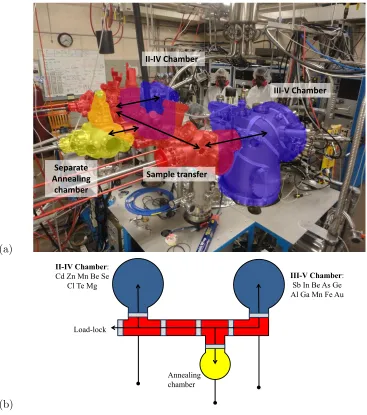
A photo of the chamber used for growth of GaAs nanowires via the Vapour-Liquid-Solid mechanism (see chapter 5) with colour overlaid indicating the purpose of the different re-gions is shown in Figure 2.3(a), and a schematic of this chamber is shown in Figure 2.3(b). This setup consists of two separate Riber 32 MBE (Molecular Beam Epitaxy) chambers connected by a sample transfer chamber some 2 metres in length. The chambers are separately dedicated to the fabrication of II-VI and III-V semiconductor samples. They
(a)
III-V Chamber II-IV Chamber
Sample transfer Separate
Annealing chamber
(b)
Annealing chamber
III-V Chamber: Sb In Be As Ge Al Ga Mn Fe Au II-IV Chamber:
Cd Zn Mn Be Se Cl Te Mg
[image:36.596.102.469.234.649.2]Load-lock
Figure 2.3: VLS Chamber
(a) Photograph of UHV chamber for MBE growth with false colour added to indicate the different regions. The blue areas are two Riber 32 MBE chambers for growth of II-VI and III-V materials. They are connected by the sample transfer corridor in red, and in yellow is shown an additional annealing chamber.
Chapter 2. Experimental Methods 13
are evacuated by a combination of ion, cryogenic and titanium sublimation pumps. In addition, there is a an inner wall around the sample space (but not obstructing deposi-tion flux and sample manipuladeposi-tion) through which liquid nitrogen is circulated. This is designed to trap residual molecules and minimise pressure in the vicinity of the sample. Samples are attached to a molybdenum block using a small quantity of melted indium. When attached to the sample stage the molybdenum blocks can be rotated and heated during deposition. Most of the sources are evaporated by means of Knudsen Cells or K-Cells. These are ceramic pockets that are resistively heated to evaporate the material within them. Fe and Au could also be deposited by means of an e-beam evaporator. Arsenic is introduced into the chamber using an Arsenic Cracker source, which first sub-limates solid As and then passes the gas through a heating system whose temperature determines the species of As molecule that will eventually make its way into the depo-sition chamber. As4 and As2 were produced by using a cracker temperature of 600◦C and 1000◦C respectively.
2.1.3 Tube Furnace
Two tube furnaces were used for different purposes during the studies below. A Py-rotherm tube furnace with quartz tube was used for oxidising Si samples prior to their use as a substrate for nanowire deposition. Samples were heated to 830◦C for 15 hours in the presence of high purity O2 at atmospheric pressure. This is carried out to form an oxide layer approximately 100 nm thick at the surface of the sample. AFM is used to confirm that this procedure does not affect surface morphology.
A second tube furnace (MTI GSL1600 XL) was used for annealing sapphire substrates. Annealing was carried out at atmospheric pressure and at a temperature between 1000◦C and 1550◦C. Temperature was regulated and calibrated using both S-type and B-type thermocouples. The tube and crucible were both of high-purity alumina to prevent contamination of the sample surface. Cylindrical alumina bricks were used to close the tube openings to further reduce contamination and to allow a more homogeneous temperature profile.
2.2
Characterisation of Sample Morphology
2.2.1 Atomic Force Microscopy (AFM)
Chapter 2. Experimental Methods 14
of the surface. Two AFM devices are available to the group; a Solver Pro, NT MDT and an Asylum Research MFP-3D. In AFM, a very sharp tip (radius 20 nm or less) at the end of a silicon cantilever is lowered to the surface of the sample to be investigated. The tip experiences van der Waals forces due to its proximity to the surface, and the cantilever is bent slightly downwards as a result. A laser beam in the visible range is directed at the cantilever whose top surface is highly reflective. The reflected laser light is measured using a photodiode, thus measuring the deflection of the cantilever. The tip is rastered across the surface using piezoelectrics to measure the height of the surface at each point. All the AFM imaging in this study was conducted in semi-contact or “tapping” mode. In this mode, the cantilever is made to oscillate by applying an alter-nating electric field, with an amplitude of approximately 100-200 nm. This amplitude is reduced when the tip is in the vicinity of the sample surface due to van der Waals forces, dipole-dipole coupling and electrostatic interactions. Operating an AFM in semi-contact mode allows concurrent phase imaging. This procedure measures the phase difference of the oscillating tip to the driving signal which is material dependent.
2.2.2 Scanning Electron Microscopy (SEM)
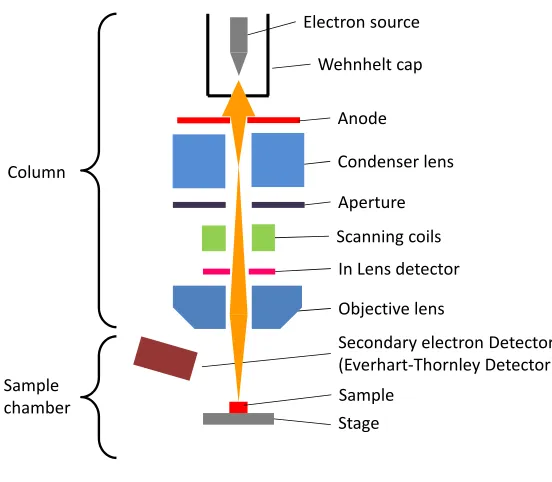
Scanning Electron Microscopy is a very common tool in the area of nanoscience research. It provides a quick and relatively easy method for morphological analysis with some degree of elemental contrast incorporated. It is adaptable to encompass a range of other functions such as quantitative chemical analysis and electron beam lithography (EBL). Standard SEMs such as those used throughout this work (Zeiss Ultra Plus, Zeiss Supra 40, FEI-Magellan 400 FESEM) are able to resolve details as small as 3 nm. A schematic illustrating the design of an SEM is shown in Figure 2.4. An SEM consists of an evacuated chamber in which the sample is mounted, an electron source, a series of lenses and scanning coils to focus the electron flux into a collimated beam and electron detection apparatus. The electrons are produced via Schottky Field Emission at a heated source (usually a tungsten filament) near the top of the electron column. The Wehnelt cap is a cylinder surrounding the electron source at a voltage, known at the extraction voltage, which can be varied to control the emission current. The total voltage can be as high as 30 kV, as determined by the voltage at the anode. The electron beam is focussed using a series of electromagnetic lenses, while the position where it strikes the surface is controlled by electrostatic scanning coils.
Chapter 2. Experimental Methods 15
Electron source
Wehnhelt cap
Anode
Condenser lens
Objective lens Aperture
Scanning coils
In Lens detector
Secondary electron Detector (Everhart-Thornley Detector)
Sample
Stage Column
[image:39.596.174.450.86.327.2]Sample chamber
Figure 2.4: SEM Schematic
Schematic of a Scanning Electron Microscope showing the various components.
excited by the incident beam, called the “interaction volume”, as well as the variety of electrons or x-rays that are being measured. The radius of the effective interaction volume (RIV) will depend strongly on the energy of the incident electrons (E), the density of the material under investigation (ρ), the relative atomic mass (A) and atomic number (Z). the following equation for the radius of the interaction volume was derived by Kanaya and Okayama and is used here as a guide [27]:
RIV =
0.0276A E1.67
ρ Z0.89 (µm) (2.1) As can be seen, increasing the voltage will increase the interaction volume resulting in poorer resolution, but in practice a more intense signal is achieved due to the greater number of backscattered and secondary electrons (see below) that can be measured. The signal intensity can also be improved by increasing current, but the drawbacks may include damaging the sample surface either through heating or build-up or electric charge (a common phenomenon especially for poorly conducting samples known as “charging”). These are important concepts to understand when using an SEM and analysing data, because the region being probed may be orders of magnitude greater in diameter than the beam spot size. In the following, the different types of electrons produced and the main detection methods associated with them shall be discussed.
Chapter 2. Experimental Methods 16
Sample Vacuum
SE
BSE Characteristic
X-rays Incident
electron beam
Figure 2.5: SEM Interaction Volume
The relative sizes (not to scale) of the interaction volume for different types of electron and x-ray measurement that may be carried out using an SEM. Red indicates the interaction volume for secondary electron, green indicates back-scattered electrons and blue indicates characteristic x-rays.
sample surface a large number of secondary electrons (SE) are produced in a cascade-like fashion due to inelastic collisions of the PE. Their energy is low (typically<50 eV) and thus their mean-free path and depth from which they can escape is small (red region in figure 2.5). The spatial resolution is therefore very good. The Everhart-Thornley detector is the most common method of detection for SE. This consists of a metal grid at a positive voltage to attract the low energy SE. The SE are accelerated by the grid towards a solid-state detector. Since the Everhart-Thornley detector is positioned to one side of the sample chamber it draws a larger signal for surfaces that are tilted towards it than those tilted away from it. Thus this imaging mode has an intrinsic slope-dependent contrast which allows good imaging of topographical features.
Some PE hit the sample surface and collide elastically retaining much of their incident energy. These are known as backscattered electrons (BSE). Since they have a high energy they have a high mean-free path, and so the resolution associated with BSE is poorer than for SE (green region in figure 2.5). Since the angle through which BSE are scattered is small they form the bulk of the electrons measured by the “In Lens” detector, which is situated inside the pole-piece of the electron column. The proportion of PE which are backscattered will depend on the atomic mass of the material under inspection, so in many circumstances In Lens detection offers a useful intrinsic elemental contrast.
Chapter 2. Experimental Methods 17
that the resolution associated with x-ray analysis is relatively poor (blue region in figure 2.5) due to the high energies required to generate the x-rays and the relative ease with which x-rays can escape from deep within the sample.
2.2.2.1 Additional SEM capabilities
• Electron Beam Lithography (EBL)
Electron Beam Lithography is a technique used to “draw” patterns of metal onto substrates with very small dimensions; as low as 20 nm using the latest equipment. Often the patterns are designed to form a circuit enabling nanoscale conductivity measurements, but may also be used to design a grid of similar shapes such as the nanoparticle arrays discussed in chapter 5. EBL begins with spin-coating a thin layer (≈10 nm) of “resist” (polymer liquid) onto the sample surface, which is then set by baking the sample at 180◦C. The key feature of the resist (Polymethyl methacrylate, PMMA) is that it will degrade (the polymer chains are broken down) when exposed to the electron beam. The SEM is used to expose regions of the surface to the electron flux in an automated manner according to a pattern de-signed by the user. The degraded regions are then removed by rinsing the sample in a solvent known in this procedure as the “developer” (Methyl isobutyl ketone, MIBK). A resist which is removed in regions exposed to the beam, such as PMMA, is known as a ‘positive’ resist. ‘Negative’ resists also exist, wherein the only re-gions that remain post-development are those that are exposed to the beam during exposure. Following development, a layer of the desired film is then deposited over the entire sample surface, including regions covered and uncovered by the remain-ing resist. The rest of the resist is removed usremain-ing acetone, leavremain-ing the deposited layer attached only in regions where the resist had been etched away.
• Energy Dispersive X-Ray Spectroscopy (EDX)
Chapter 2. Experimental Methods 18
required to specify which elements they expect to see in their sample. The PE must have sufficient energy, greater than the “critical excitation energy” needed to eject the inner electrons, in order to make each characteristic peak accessible. In practice the acceleration voltage of the PE is as large as possible, often some 20 or 30 kV in order to maximise the intensity of each peak. This in turn means that the interaction volume is several times greater in diameter than the beam spot size, meaning that resolution is negatively affected.
2.2.3 Transmission Electron Microscopy (TEM)
TEM, like SEM, is a ubiquitous tool in the area of nanoscience research. It can be used to provide images with sub-nanometre resolution and can resolve the crystal structure of crystalline solids. Since it relies on electron transmission, this technique is applicable only to samples that are sufficiently thin for a perceptible proportion of the incident electrons to pass through. The sample may be cut into a narrow wedge using a FIB (Focussed Ion Beam) or if the sample under investigation consists of a collection of nanoparticles then these may be dispersed onto a special grid which is almost transparent to the incident electrons. The TEM is operated at high voltages (≈300 kV) to maximise electron transmission and resolution. Like the SEM, the TEM consists of an electron source, a column with lenses and focussing apparatus and sample stage. However, the voltages involved are much larger and since transmitted electrons are measured, the detection equipment lies beneath the sample holder. Another key difference, as mentioned above, is that the electron beam hits the sample surface not as a finely focussed point but as a column that illuminates the entire region being imaged at once. The most common imaging mode is Bright-Field imaging, wherein electrons that have a very small angle of scattering are detected. In this mode empty space appears bright (hence the name) while thicker regions appear darker.
Chapter 2. Experimental Methods 19
2.2.4 Scanning Transmission Electron Microscopy (TEM)
Both SEM and TEM microscopes may offer STEM mode. As the name suggests, this tool deals with electrons that pass through the sample rather than those that are scattered backwards from the surface. Since this procedure is very similar to the conventional Transmission Electron Microscope (TEM) which is discussed above, here just the main difference distinguishing the two will be outlined, namely that while the TEM illuminates the entire region being imaged with a column of electrons, in STEM the surface is rastered by a point-like beam of electrons. STEM mode on a SEM is useful since it can be used to provide some information on the structure of the sample below the surface. On a TEM, the resolution is usually worse when switching to STEM mode, but doing so allows the user to carry out high resolution EDX linescans.
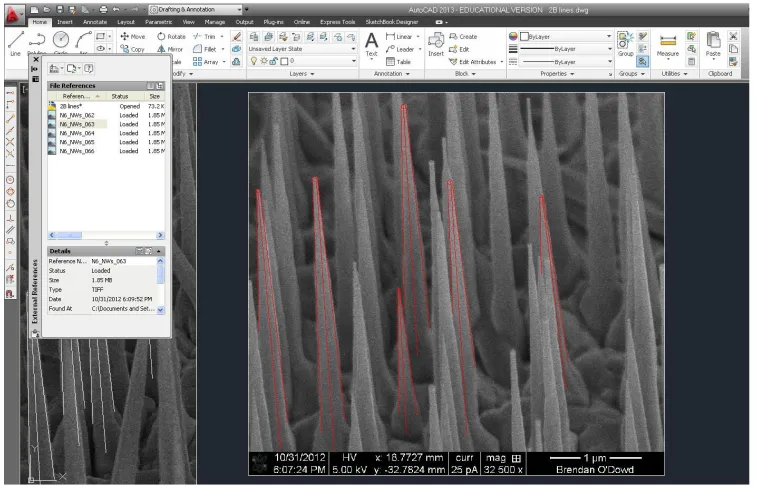
2.2.5 Statistical Analysis of Nanoparticle Dimensions
When nanoparticle arrays were grown with slightly different growth parameters resulting in variations in their shape and separation, it was necessary to quantify the findings by means of an accurate, statistical analysis of specific dimensions of the nanoparticles. Likewise, for the GaAs NW arrays, a quantitative analysis was needed to study the effect of growth conditions on the size and shape of the resulting NWs. The conventional approach to this task would be to convert an image to a binary black and white format based on some threshold parameter and then use software to automatically identify shapes and distances. However, this is not well-suited to more complicated images where human judgement is required to identify features and where only a proportion of features are unobscured and suitable for measurement. In order to carry out these surveys, AutoCAD software was used (AutoCAD 2013, Autodesk). While this software is primarily intended for product design and construction planning, its huge array of tools makes it suitable for image analysis. Images taken using the SEM were opened in AutoCAD and scaled to size so that measurements could easily be read off. Then lines, circles or ellipses are drawn over the features of interest until a statistically significant quantity were included. Figure 2.6 shows a screenshot of the program being used to measure the lengths of cone-shaped GaAs NWs, as well as the diameter of their tips and the angle near the top of the cone.
Chapter 2. Experimental Methods 20
Figure 2.6: Statistical Analysis using AutoCAD
Screenshot of AutoCAD software being used to specify multiple features in an SEM image of an array of GaAs NWs. The dimensions of the features may be extracted to a data file using the software for quantitative analysis, which can also correct for shortening caused by the viewing angle as in the case above.
2.3
Magnetic Characterisation
2.3.1 Vibrating Sample Magnetometer (VSM)
Chapter 2. Experimental Methods 21
2.3.2 Alternating Gradient Field Magnetometer
In short, while a VSM causes the sample to oscillate and measures the induced field, the AGFM applies an oscillating gradient field and measures the resultant vibration of the sample. Again a magnet applies a fixed field on the sample (fixed in the timeframe of the individual measurement), although in this case an electromagnet with maximum field of 1 T is used rather than a superconducting magnet. The alternating gradient field is produced by smaller coils positioned at the pole pieces of the electromagnet. This exerts a force f on the sample according tof =∇(m·B0) where m is the magnetic moment
and B0 is the applied magnetic field. The frequency of the oscillating gradient field
is chosen to be equal to the mechanical oscillating resonance frequency of the sample together with its non-magnetic holder.
The disadvantages of this system are that it is limited to room temperature measure-ments and that the maximum field is only 1 T. However, since the applied field can be changed rapidly there are several advantages to the AGFM. The first is that samples can be demagnetised by alternating the direction of the applied field, starting from a value large enough to saturate the sample and finishing at zero applied field with as many intervening steps as practically possible [28]. This process is known as AC demagnetisa-tion. In effect, this process divides all of the domains into two groups with magnetisation pointing in opposite directions according to the magnitude of their switching field. By making the increments of the decreasing field magnitude small enough the end result is a practically random orientation of all the domains.
Another advantage is the potential to carry out additional modes of measurements, two of which are outlined below.
2.3.2.1 Addition AGFM Measurements
• Remanence Measurements
Chapter 2. Experimental Methods 22
H M
MR ( H1)
MD(H1 )
H1
H1
MR ( ∞ )
Figure 2.7: Schematic for findingMR(H) andMD(H).
Here a hysteresis loop for a hypothetical system is shown in blue. Also shown are curves in red which illustrate howMRandMD are experimentally found for an applied fieldH1.
sample is saturated in (say) the +x direction. Then a fieldH is applied in the−x direction and removed, whereupon the DC demagnetisation remanence, MD(H) is measured. Figure 2.7 illustrates howMRand MD are found on anM−H graph for a hypothetical ferromagnetic system.
Also shown in this figure is the remanence for infinite applied field (or in practice a field high enough to saturate the sample). This is labelled ‘MR(∞)’ and is in actuality just what is normally understood as the remanence, and is, of course, equal toMD(∞). Normalised versions of MR and MD are defined as follows:
mR(H) = MR(H) MR(∞) mD(H) = MD(H) MR(∞)
(2.2)
• First Order Reversal Curves (FORCs)
To measure a first order reversal curve the sample is first saturated in, say, the +x direction. Then the applied field is reduced to a value Ha known as the “reversal
field”. The magnetisation is then recorded as the applied field, now labelled Hb
is increased from Ha back up to saturation. This is repeated for values of Ha
Chapter 2. Experimental Methods 23
H M
Ha
M(Ha , Hb) Hb
Figure 2.8: Schematic for finding FORCs.
A hysteresis loop for a hypothetical system is shown in blue. The orange curve illustrates the applied field being reduced from a saturating field to the reversal fieldHa. While this curve is part of the procedure, it is not part of the measurement, and recording this curve is not necessary. The red curve shows a single first order reversal curve (FORC), which measures the magnetisationM(Ha,Hb) as the applied fieldHb is increased fromHa back up to saturation.
2.3.3 Ferromagnetic Resonance (FMR)
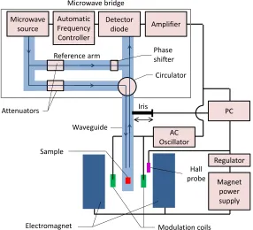
Room temperature FMR measurements of Fe nanowire arrays and Fe-coated GaAs nanowires were carried out using FMR (Bruker EMX, operated at 9.47 GHz) at the University of Notre Dame, Indiana, USA. Further analysis of the Fe nanowire arrays was conducted at the Institute of Magnetism at the National Academy of Sciences in Kiev, Ukraine. These measurements were also carried out at room temperature using an X-band (9.44 GHz operating frequency) ELEXSYS E500 spectrometer, which includes an automatic goniometer for sample rotation.
The mathematical background for the role of the FMR as a probe of magnetic anisotropy is given in section 4.1.1.1. Here is given a qualitative discussion of its operation for use as a probe of magnetic anisotropy and a description of the hardware involved. A schematic of the experimental setup is shown in figure 2.9. The sample is loaded into a quartz tube, preferably oriented with one of its principal axes parallel to the tube axis so that the resonance field can be probed as the sample is rotated about a known axis. The tube is filled with He gas, sealed and inserted into its holder between the poles of the electromagnet. The magnet applies a static field H0, where ‘static’ implies that it
Chapter 2. Experimental Methods 24
Modulation coils Electromagnet
Sample
Waveguide Microwave
source
Reference arm
Circulator
Attenuators
Phase shifter Microwave bridge
Regulator
Magnet power supply Hall
probe Iris
AC Oscillator
PC Amplifier
Detector diode Automatic
[image:48.596.138.424.86.346.2]Frequency Controller
Figure 2.9: FMR Setup Schematic
not just the applied field but also included a contribution from the internal demagnetising field, Hd. The magnitude of the demagnetising field depends on the demagnetising
factors of the sample, and thus the resonance frequency will depend on the magnetic anisotropy of the system. In addition to the ‘static’ magnetic field, there is a time-varying field of lower amplitude produced by modulating coils so that the reflected microwave amplitude is modulated at the same frequency. The frequency of this modulating field is usually 100 kHz. The signal to noise ratio is improved by reading the diode current with an amplifier locked in to the AC oscillator. In addition, this causes the output signal to be the derivative of the actual absorbance spectrum. While it can be easily integrated, it is often easier to accurately extract data such as absorption peak width, from the differentiated signal provided.
Chapter 2. Experimental Methods 25
Chapter 3
Template Preparation and
Glancing Angle Deposition
This chapter covers the fabrication procedure for ordered arrays of nanowires and nano-particle arrays, which consisted of two key procedures. The first is the preparation of a step-bunched substrate, which was achieved by annealing vicinal silicon or sapphire (α -Al2O3). These procedures are outlined in sections 3.2 and 3.3 respectively. In the case of the preparation of sapphire templates, the procedure and apparatus are almost identical to that used in a study by Verre et al. [29] and so some representative results will be shown rather than an in-depth study into the dependencies of the various parameters.
The second key procedure is the deposition at glancing angle onto the step-bunched templates, which is described in section 3.4. As shall be shown, the advantages of this approach include its ability to define a well-ordered nanowire array with good control over the width, separation and thickness of the wires, and its applicability to a range of choices for nanowire material as well as substrate material.
3.1
Background
The fabrication and study of nanowires is a very wide and active area of research, with a myriad of proposed applications. As mentioned in chapter 1, the study of magnetic nanoparticles is important for the hard disk dive (HDD) industry since it provides a means for examining and overcoming the obstacles associated with device minimisation, as well as exploring the range of exciting effects at the atomic level that can be employed in future designs. Other areas with application potential include domain wall logic devices [20, 21], magnetic sensing [24], devices for high-frequency signal processing [23],
Chapter 3. Template Preparation and Glancing Angle Deposition 28
spin-polarised electronics [22] and devices employing giant magnetoresistance (GMR) [30].
The ubiquity of Si for production of electronic devices makes it attractive for use as a template for growth of nanowires for two reasons. Firstly, because of the existing knowl-edge and experience within the scientific community of working with and understanding this material, and secondly due to the potential for bridging the gap between prototype and device by using the existing substrate of choice of the electronics industry. While similar templates may be produced using oxides or metals, these specific advantages make Si attractive for use as the underlying material for our arrays.
There is much interest in producing magnetic nanowires that have a width on the order of a few nanometres, but they should also be sufficiently thick in order to overcome superparamagnetism at room temperature if they are to be of use in practical applica-tions. Superparamagnetism is when a ferromagnetic particle is small enough for thermal effects to cause its magnetisation to randomly flip 1[31, 32]. This will be discussed in more detail in section 4.1.3, but for now it suffices to say that the wire thickness will typically need to be on the order of nm in order to exhibit ferromagnetic behaviour at room temperature, and this is a significant challenge for various methods of nanowire fabrication.
Production of arrays of nanowires can be done using bottom-up or top-down approaches. A typical top-down approach is Electron Beam Lithography (EBL). Feature size using EBL is limited by beam spot size, around 20 nm diameter for most up-to-date devices. EBL is also a relatively slow and expensive process.
Bottom-up approaches, with the possibility of smaller feature size and greater through-put, are an attractive option. A fast and cheap self-assembly method for generating nanowire arrays would potentially allow for an exploration of the key dimensions and how they affect the behaviour of the overall system. Findings from such experiments are of academic importance since it provides an avenue for exploration of nano-scale magnetic processes, and from an industrial perspective it is also useful since it presents a ‘playground’ in which to quickly and easily probe certain dependencies. Magnetic nanowire arrays of varying wire/stripe width ranging from single atom (1-D atomic chains) to several hundred nm are reported on a variety of templates. Vertical pillars of Fe, Ni and Co have been formed in porous alumina [33–38]. In this approach, alumina is anodized in an acid electrolyte which results in highly regular vertical cavities through-out the alumina layer. A similar array of vertical pores can be produced by exposing polycarbonate films to a beam of particles which leave tracks in the film. These tracks
1Strictly speaking, the definition of superparamagnetic depends on the measurement time. For