INTERNALDOCUMENT
AN AUTOMATIC ZERO-LEVEL SETTING CIRCUIT A part of the electronic model
for tides and storm surges S. Ishiguro
1982
[This document should not be cited in a published bibliography, and is supplied for the use of the recipient only].
INSTITUTE OF aCEAIMOGRAPHIC SCIENCES
%
INSTITUTE OF OCEANOGRAPHIC SCIENCES
Wormley, Godalming, Surrey GU8 5UB
(042-879-4141)
(Director: Dr. A. S. Laughton, FRS)
Bidston Observatory,
Birkenhead,
Merseyside L43 7RA
(051-653-8633)
(Assistant Director: Dr. D. E. Cartwright)
Crossway,
Taunton,
Somerset TA1 2DW
(0823-86211)
INSTITUTE OF OCEANOGRAPHIC SCIENCES INTERNAL DOCUMENT 160
AN AUTOMATIC ZERO-LEVEL SETTING CIRCUIT A part of the electronic model
for tides and storm surges S. Ishiguro
1982
CONTENTS
1. Introduction 3
2. Principle 3
3. Design of the circuit 4
4. Physical arrangement 7
5. Calibration of the circuit 8
6. Conclusions 12
ABSTRACT
A circuit which separates an arbitrary-waveform voltage from an arbitrary dc leyel has been described. This circuit contributed' significantly to reducing the time of processing the data of responses of sea level to external forces. The circuit will have general
1. INTRODUCTION
'Electronic Model' is a system of simulating tides and storm surges for oceanography. Operation of the system includes obtaining a response (e.g. sea level) to an external force (e.g. the stress of a wind on the sea surface). In the main computing network of the system, the response is, represented by an analogue voltage which is superimposed on a dc vol-tage. Due to an instrumental reason, the dc voltage varies from grid to grid in the network. Therefore, the zero-level of the response has to be determined individually. This paper describes a circuit which deter-mines the zero level automatically. This increases the efficiency of operation when a large number of responses are processed.
2, PRINCIPLE
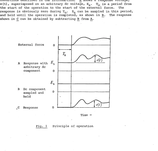
Fig. -1 shows the principle of the operation which satisfies the conditions described in the introduction. A shows a response voltage, eCt), superimposed on an arbitrary dc voltage, E^. TQ is a period from the start of the operation to the start of the external force. The response is obviously zero during T^. E, can be sampled in this period, and held until the operation is completed, as shown in B^.
shown in C can be obtained by subtracting B from A.
The response
External force
A Response with arbitrary dc
component 0
B Dc component sampled and ® held
,C Response
— — •
To
e{t)
•
[image:5.598.51.573.321.819.2]Time ->
3. DESIGN OF THE CIRCUIT
The circuit is described here in two parts:
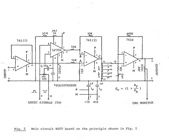
3.1 Main circuit
Fig. 2 shows circuit BD50 which has been based on the principle described in Chapter 1. 741(1) is a voltage follower to which a voltage representing a 'response with a dc component' (A in Fig. 1) enters. This output is divided into two parts. The first part enters into a sample-and-hold circuit, LF398, This voltage is sampled only when its pin 8 is logically high (+5V) , and held for a short period. CI is the holding capacitor. VR2 is for adjusting a dc offset. C2 and VRl are for adjusting an ac offset, and require a voltage having a reversed polarity to that of the logic voltage supplied to pin 8.
The second part of the output of 741(1) , A, and the output of LF398, B^, enter the 741(2) so that its output, is equal to A - B_. C is scaled by a step-potentiometer and an output amplifier, 74IS.
741(1)
2 2 K I K
-/Wv tp 4 4 0 K
/At-741(2)
l O K A
*POLYSTYRENE
i
[image:6.602.19.567.317.771.2]LOGIC SIGNALS (5V) - 1 5 + 1 5 CRO MONITOR
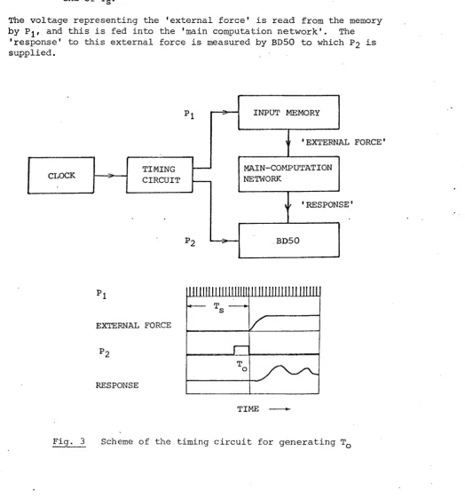
3.2 Timing circuit
Although the pulse width of TQ (see Fig. 1) is not critical, it is important that the end of the period T^ is exactly the same as the start of a voltage representing an 'external force'.
Fig. 3 shows a scheme to satisfy this condition. The ' input memory' stores a waveform representing an 'external force', with an undisturbed period, Tg. The timing circuit, which is controlled by a clock, generates two types of pulse:
Pj : Pulses to read the whole contents of the input memory, including the undisturbed period.
P2 ; A single pulse having the width of TQ which ends at the end of Tg.
The voltage representing the 'external force' is read from the memory by Pj, and this is fed into the 'main computation network'. The
'response' to this external force is measured by BD50 to which P2 is supplied.
CLOCK TIMING
CIRCUIT
INPUT MEMORY
\ ' 'EXTERNAL FORCE
MAIN-COMPUTATION NETWORK
f 'RESPONSE'
BD50
EXTERNAL FORCE
RESPONSE
l l ! l ! i l l H I ! ! l l ! ! ! l l
[image:7.595.46.571.261.823.2]TIME
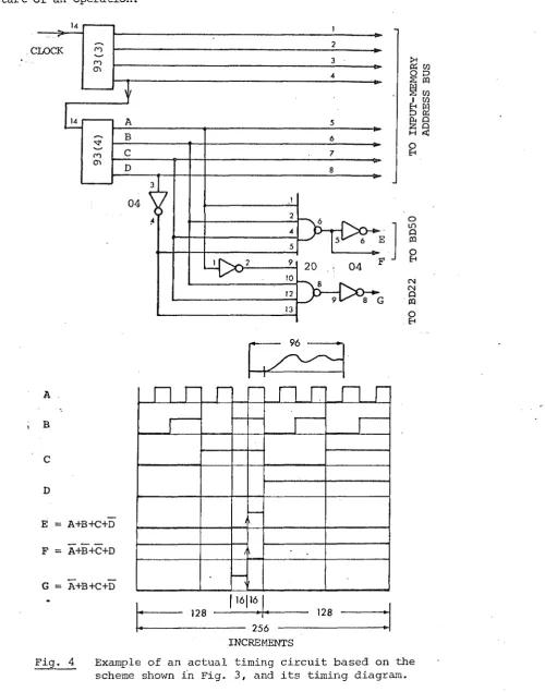
Fig. 4 shows an example of an actual circuit based on the scheme shown in Fig. 3. The counters, 93(3) and 93(4) are built on board Ml of the input memory. The outputs from E and F are fed into terminals 9 and 10 of BD50 respectively, and G into BD22 for synchronizing the start of an operation.
CLOCK
04
20 04
ro
is
§ w
ii
H <
g o in Q CQ g CM Q g A B
E = A+B+C+D
F = A4B+C+D
G = A^+B+C+D
128
16 16
128
256 INCREMENTS
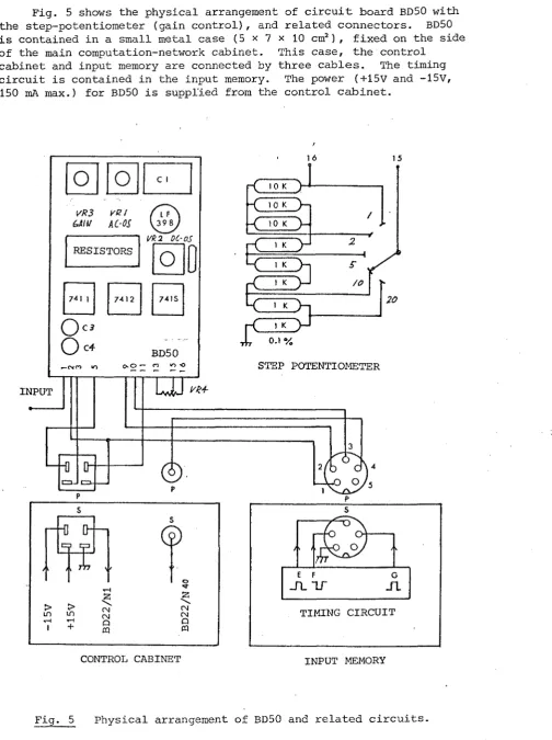
PHYSICAL ARRANGEMENT
Pig. 5 shows the physical arrangement of circuit board BD50 with the step-potentiometer (gain control), and related connectors. BD50 is contained in a small metal case (5 x 7 x 10 cm'), fixed on the side of the main computation-network cabinet. This case, the control
cabinet and input memory are connected by three cables. The timing circuit is contained in the input memory. The power (+15V and -15v,
150 mA max.) for BD50 is supplied from the control cabinet.
INPUT
-CJOTJ
-C 10 K J—
yR3 Kg/
&.AII/ AC-OS -C 10 K
")-W2 DC-OS
5
7 4 I S
74 12
BD50
STEP POTENTIOMETER
E F G
- T L T T Si
TIMING CIRCUIT
[image:9.597.56.561.107.783.2]CONTROL CABINET INPUT MEMORY
8
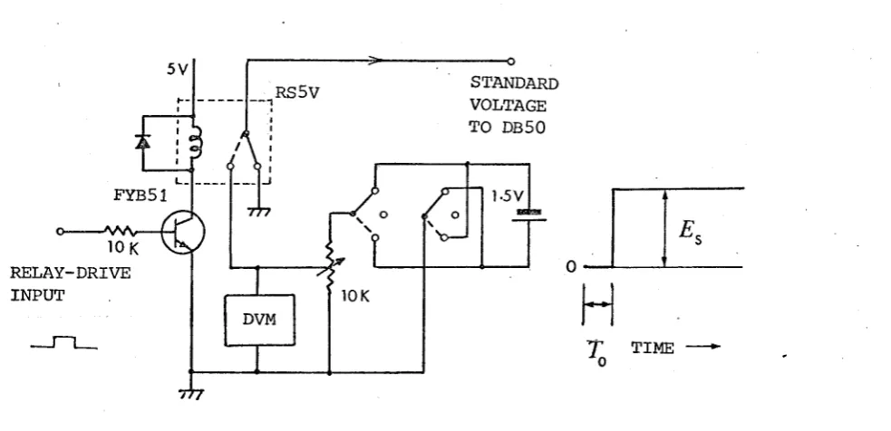
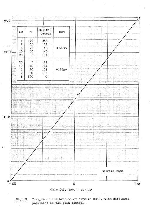
5. CALIBRATION OF THE CIRCUIT
The voltage gain of circuit BD50 is adjusted by VR3 (see Fig. 2) , after the dc offset and ac offset of LF398 have-been adjusted by VR3 and VR2 respectively. For the calibration of the voltage gain, a circuit shown in Fig. 6 was used.
STANDARD VOLTAGE TO DB50
FYB51 • A W
1 0 K
RELAY-DRIVE INPUT
E.
H
T TIME
0
[image:10.595.53.564.62.802.2]7 7 7
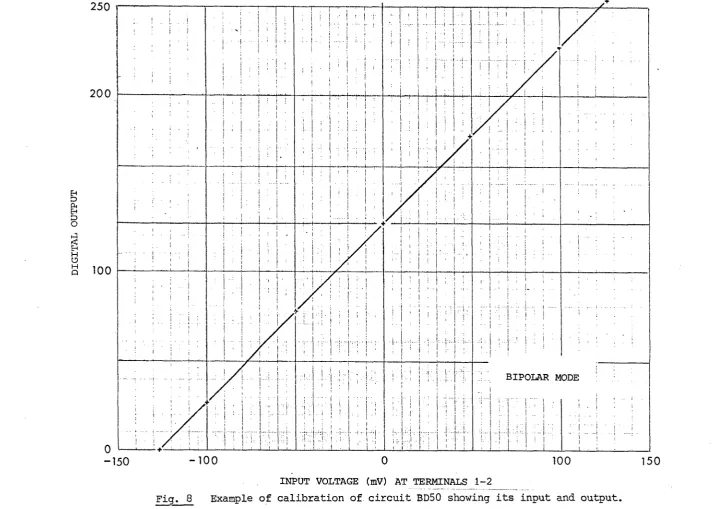
Fig. 6 Calibration circuit for BD50, and its standard waveform.
This calibration circuit generates a standard step-voltage Eg with a zero-volt period of T^, as shown in Fig. 6. The value of Eg can be chosen between +1.5V and -1.5V, and the voltage can be read by a dc range of a digital voltmeter with a 4.5-digit accuracy. In order to obtain TQ, the logic.pulse fed into terminal 9 of BD50.(see Fig. 2) should also be fed into the relay-drive input of the cali-bration circuit.
With the calibration circuit, the output of BD50 should be digitized by the ADC on BD22. Its digital output should be read by an appropriate instrument. Then the gain control VR3 should be adjusted to obtain the following conditions:
Input (mV) -127 0 +127 Output (digits) 254 127 0
At gain control position 1, and BIPolar mode of the ADC.
[image:10.595.56.548.174.412.2]254
1
i
O H o 127/
/
/
/
/
/
/
/
/
/
- 1 2 7 0 127 254
[image:11.595.49.581.35.840.2]INPUT VOLTAGE (mV) AT TERMINALS 1-2 •
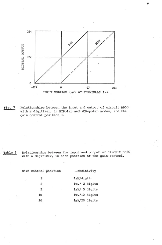
[image:11.595.69.566.69.451.2]Fig. 7 Relationships between the input and output of circuit BD50 with a digitizer, in BIPolar and MONopolar modes, and the gain control position 1.
Table 1 Relationships between the input and output of circuit BD50 with a digitizer, in each position of the gain control.
Gain control position
2 5 0
200
i
g
H
U
H
O 100
BIPOLAR MODE
- 1 5 0
INPUT VOLTAGE (mV) AT TERMINALS 1-2
[image:12.846.65.784.23.532.2]150
1 1
2 5 0
I
t
H
O
H
O
200
— sw %
Digital
Output 100% -
-1 100 255
2 50 191
5 20 153 +127mV
10 10 140
20 5 134
-r- 20 5 121
- - - - 10 10 114
-"L 5 20 101 -127mV
2 50 63
1 100 0
100
BIPOLAR MODE
[image:13.598.44.555.44.754.2]GAIN (%), 100% = 127 mV
12
6. CONCLUSIONS
In order to obtain information of sea-level responses to wind fields and atmospheric pressure fields, large amounts of data expressing the responses have to be processed. The circuit des-cribed in this paper contributed significantly to reducing the processing time of operations.
The circuit will have general applications.