© 2019, IRJET | Impact Factor value: 7.211 | ISO 9001:2008 Certified Journal
| Page 1226
Design Verification of Universal Memory Controller IP Core (UMC)
using System Verilog Architecture
Jagadeesha Kolour
1, Nagendra Reddy
2,
Venkata Siva Reddy
31,2,3
Dept. of ECE Engineering, Reva University, Karnataka, Bangalore-India, 560064
---***---Abstract -
An The word Design Verification itself tells that this paper does not involve Designing of Memory Controller Core, for the verification one needs its Design Specification Sheet to understand the working of the design so that it can be simulated in the Advanced Verification tools. The RTL logic is written in Verilog and the aim is verify every aspect of the design and to generate regression test cases in the Test-bench to obtain 100% Functional Coverage using System Verilog (SV).To understand Verification methodology first step is to understand about UMC IP Core specification and its role in as an intermediate Communication device which rest between memory & processor. MC commutes between the processor and memory accordingly as when the processor request for memory, each different type of memories connected at other end of MC has its own signals for communication which is taken care by the MC. Features of UMC includes SDRAM, SSRAM, FLASH, ROM and many other devices supported,8 Chip selects, each uniquely programmable, Flexible timing to accommodate a variety of memory devices, Burst transfers and burst termination, Supports RMW cycles, Performance optimization by leaving active rows open, Default boot sequence support, Dynamic bus sizing for reading from Async. Devices, Byte parity Generation and Checking, Multi Master Memory bus support, Industry standard WISHBONE SoC host interface, Up to 8 * 64 Mbyte memory size, Supports Power down Mode,
Key Words: UMC, DUT, WISHBONE, SDRAM, SSRAM, SYNC
1. INTRODUCTION
The processor cannot really understand the type of memory connected to it and might not even generate the right signals need in order to fully communicate with different types of memory, thus there is a need for an intermediate device which seats between processor and the memories to handle such issues.
For SOC having different types of memories like SDRAM, DRAM, SSRAM, FLASH etc.., it will require different types of memory controllers for each memory types. Which will add extra space on SOC. Universal memory controller design, improved by integration of the existing memory controller in addition of providing novel features. This make the low power consumption for the design. UMC controller design which is supporting SDRM, SSRAM and SYNC memories what we call as Universal Memory Controller. This UMC design is
having some specific function like, it has 8 chip select line and it support different types of memory. Single memory controller which is supporting different memories, for this UMC design, verification is done by generating a test cases in system Verilog language.
2. Universal Memory Controller
[image:1.595.314.553.304.417.2]F
Fig 1: Block diagram of UMC
As can be seen in the above block diagram the processor communicates the UMC via wishbone interface and memories linked to the UMC are communicated respectively as per the signal required by the memories and the request generated via processor. Wish bone block is a place where we are verifying the UMC by checking read and write dada matching, if both read and write data matching then UMC is working properly and hence verification is done.
Memory modules containing a different types of memory like SDRAM, SSRAM, and SYNC. These memories attached to the UMC through memory interface. All these memory designs are written in Verilog code, these Verilog codes are included in the top file of the system Verilog module. While verification system Verilog top modules are used.
UMC is having its own architecture design with novel feature supporting. UMC is placed between WISHBONE and memory module. These blocks are interfaced by WISHBONE interface and memory interface to the UMC.
© 2019, IRJET | Impact Factor value: 7.211 | ISO 9001:2008 Certified Journal
| Page 1227
[image:2.595.303.562.63.397.2]prospective for the designers. The Fig-2. Defines all the signals required for Wishbone interface.
Fig-2. Wishbone Interface Signals.
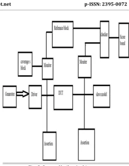
3. System Verilog Architecture
The below show Fig-3 is for the System Verification Architecture as can be seen there are various blocks which are need to coding in the tool, but the question is why Verilog only can be used and why in what way does System Verilog have advantage over Verilog. DUT Block is the Device under test i.e. the top module for which coding is done by using Verilog. If all the remaining Blocks are coded via Verilog then we have to instantiate coding by defining module name for each block, module to module communication is very hectic thus we don’t prefer Verilog for coding of other blocks instead prefer System Verilog. The main reason is System Verilog includes OOPs concepts thus defining each blocks codes in a class format provides easy way of coding as compare to Verilog.
The following Figure can be divided as two parts for master and slave configuration, the left hand side is for master and the right hand side is for the slave. Depending upon the no of slave and master the figure can be modified for different design aspects.
Fig -3. System Verilog Architecture
We can briefly define each block role independently as follows
(i) Generator Block: Responsible for generating all the signals required for all scenarios example clock & reset signals etc.
(ii) Driver/Bus function model (BFM): Routing Signals generated from the generator.
(iii)Monitor: To check signals and has inputs from coverage & assertion blocks.
(iv)Coverage Block: checking the given input to the DUT whether it’s complete or not.
(v) Assertion Block: checking at the interface as per the protocol or not i.e. indicates violation of protocols.
(vi) Reference: kind of having desire results.
(vii) Checker: Compare the outputs from the reference and DUT block.
(viii)Scoreboard: Displays the result of Checker.
4. Verification Steps
(i) Features listing down. (ii) Scenario listing down. (iii) Test plan development.
[image:2.595.37.292.127.451.2]© 2019, IRJET | Impact Factor value: 7.211 | ISO 9001:2008 Certified Journal
| Page 1228
(viii) Sanity test case bring up. (ix) Other test cases.
(x) Setting up regression.
(xi) Running regression and debugging regression results. (xii) Generating coverage results.
(xiii) Analyze coverage results. (xiv) Closing functional Coverage.
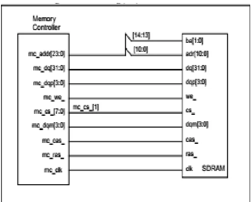
5. Different Memory Interface to UMC
5.1 SDRAM Module
Synchronous Dynamic Random Access Memory. SDRAM are faster than Asynchronous DRAM. In SDRAM whenever there is change in input side causes changes in the output side only when clock changes. SDRAM memory is divided into four banks, so read and write operations happens faster than other memories.
[image:3.595.304.561.53.305.2]Pin diagram of Memory Controller and SDRAM both blocks are interfaced by Memory interface shown in figure.
Fig -4: Interface of SDRAM with Memory Controller
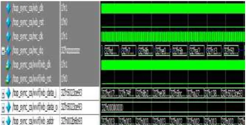
[image:3.595.35.292.383.588.2]The data from memory controller is written to the memory of SDRAM in one address location and from same address location data is read back to the Memory Controller.
Fig -5: SDRAM Read and Write
Whenever acknowledgement, cyclic and strobe pins goes high read and write operation will happens. When WB pin goes zero read operation will happen, when WB pin goes high wright happens. As the memory is synchronous the out will changes after the clock changes even there is change in input.
5.2 SSRAM module
Synchronous static random access memory. SSRAM is volatile memory it not requires the refresh cycle to store the data. As it is synchronous memory, In SDRAM whenever there is change in input side causes changes in the output side only when clock changes, output depends on clock.
[image:3.595.311.559.518.674.2]© 2019, IRJET | Impact Factor value: 7.211 | ISO 9001:2008 Certified Journal
| Page 1229
Fig -7: SSRAM Write Cycle
[image:4.595.309.559.103.251.2]This is the expected wave forms for read and wright operations. MC_WE goes wright operation will happens. And when MC_OE pin goes low read operations will happen.
Fig -8: SSRAM Read and Write
5.3 Sync
• Synchronous chip select device, it also clock dependent. All SSRAM parameters in respect to the clock and are not configurable
• MC supports standard Sync Burst, Pipelined SSRAMs with double cycle deselect. Synchronous CS devices are synchronous to memory controller’s clock.
Fig -9: Synchronous Chip Select Device Read Cycle
Fig -10: Synchronous Chip Select Device Write Cycle
[image:4.595.308.561.323.451.2]This is the expected wave forms for read and wright operation. MC_WE goes wright operation will happens. And when MC_OE pin goes low read operations will happen.
Fig -11: Synchronous Chip Select Device Read and Write
6. CONCLUSION
Memory is the main part of any processer, there are different types of memory present on SOC. To controller the different types of memory instead of using different types of memory controller for each memory, only one memory controller is used called Universal Memory Controller. In this project, the verification is done for the Memory controller which is supporting different types of Synchronous memories, along with many feathers supporting compared to old Memory Controllers. Waveform showing the results of writing data to the Memory Controller and reading it back from memory through the WISHBONE is same. The data which is given the same data is reading back hence Universal Memory Controller is working.
REFERENCES
[1] A Reconfigurable Real-Time SDRAM Controller for Mixed Time-Criticality Systems 978-1-4799-1417-3/13/$31.00 ©2013 IEEE
[image:4.595.36.289.341.476.2]© 2019, IRJET | Impact Factor value: 7.211 | ISO 9001:2008 Certified Journal
| Page 1230
[3] MohdWajid,Shahank SB, ”Architecture for Faster RAM Controller Design with Inbuilt Memory”, IEEE ,2010 ARM, AMBA Specification Rev.2.0, 1999. “Memory Controllers for Real-Time Embedded systems” Benny Akesson
[4] “Memory Controller Architectures: A comparative Study” 978-1-4799-35253/13/$31.00 ©2013 IEEE
[5] “Implementation and Verification of A Generic Universal Memory Controller Based On UVM” 2015 10th International Conference on Design & Technology of Integrated Systems in Nanoscale Era (DTIS) 978-1-4799-1999-4/15/$31.00 ©2015 IEEE
[6] IEEE Standard for SystemVerilog — Unified Hardware Design, Specification, and Verification Language. New York: IEEE 2005 (a.k.a. SystemVerilog Language Reference Manual, or LRM.)