2326 ISSN: 2278 – 7798 All Rights Reserved © 2014 IJSETR
Abstract—In this paper, design and development of algorithm
for automatic gain control (AGC) as an attenuator have been proposed. Automatic Gain Controller, as the name suggests is a gain controller device, which adjusts or control the gain to a desired or a suitable level to provide a stable output. This (AGC) technique not only enhances but also descend the attenuation as per the requirement of the device. Digital step attenuator as an AGC (TOAT – 51020+) has been tested for attenuation. This step attenuator provides the amount of attenuation according to the 3-bit TTL logic signals. The LSB of this TTL level offers the minimum amount of attenuation while the MSB offers the maximum amount of attenuation. For keeping the desired signal in a particular band of interest, in this paper, an algorithm has been proposed, according to which whenever a signal level crosses or falls below a threshold level, there will be one bit attenuation provided so that there will be rise or fall in the attenuation to keep the signal in a desired band of channel output counts, where channel output counts are the signal information range. Here, 1 bit step attenuation is of 5 dB.
Keywords—Automatic Gain Controller (AGC), RF attenuarors, Digital step attenuator, TOAT – 51020+, TTL inputs.
I. INTRODUCTION
Automatic gain control (AGC) is a technique which can be applied in many electronic devices and circuits. The average or maximum output signal level is used to maintain the gain to a desired level, which enables the circuit to work satisfactorily with a maximum range of input signal levels [5]. An attenuator is an electronic device which reduces the amplitude or power of a signal without causing a big distortion. An attenuator principle works reverseto that of an amplifier. While an amplifier provides gain, an attenuator provides a gain which is less than 1, or a loss as per requirement. Attenuators are passive devices which are made using simple voltage divider networks. Attenuation is expressed in decibels of relative power.An attenuation of 3 dB corresponds to half of the input power, while a gain of 3 dB corresponds to a doubling of the power level. A gain of -3 dB is the same as an attenuation of +3 dB, corresponding to half the original power level [1].
In this paper, RF attenuators are used. RF attenuators are a universal building block within the RF design domain. As the name implies RF attenuators reduce the level of the signal. An attenuator may be used to provide an accurate impedance match as in many attenuator it is required to provide a well-defined impedance. The attenuators may be used in a various areas, where signal levels need to be controlled and to be maintained [2].
Types of RF attenuators:
Fixed RF attenuator: As the name implies fixed attenuators have a specific value and this cannot be changed or that which cannot be altered. They may come in a variety of formats from small in line items in a similar format to connector adaptors to those in small boxes with connectors on the ends to those incorporated within equipment’s.
Switched RF attenuators: Switched RF attenuators are widely used in test systems where levels may need to be changed or altered. They are often seen as small boxes markedwith a number of switches, typically with switches for providing the attenuation as 1, 2, 4, 8, etc. dB. Switched attenuators may also be found in items of test equipment to change the levels as needed.
Variable RF attenuators: variable RF attenuators are normally used in applications where it is necessary to continuously vary the level of a signal or where signal variations are required. Typically they provide a continuous level change by varying an analogue voltage on the input control line or by showing the variation within the input signal range.
When designing or using an RF attenuator it is necessary to be able to specify it to ensure that an attenuator with the correct parameters and capacity is obtained. While some of the major
Design and Development of algorithm for AGC
as an Attenuator
Disha Singh, Mohammed Arifspecifications required for the attenuator are detailed below, which are the important parameters required during attenuators use, these are [9]:-
• Attenuation: This is one amongst the importantspecifications for an RF attenuator. Attenuation is the ratio between the output and the input power levels and is typically cited in decibels (dB) [7].
• Attenuation accuracy: It is often necessary to know the accuracy of the level of theattenuation of the attenuator. In specific with the applications where equipment’s are tested, the attenuation accuracy is of prime important. In these cases a tolerance on the nominal (theoretical) level of attenuation will be given, which will provide its accuracy in terms of attenuation.
• Frequency response: The level of attenuation of an attenuator will vary with the frequency. This can result from the frequency dependence of the resistors or other components used in the RF attenuator.
• Impedance: RF attenuators will be designed for use in systems with agiven characteristic impedance. 50 ohms which is the most common, although 75 ohms is also used, and it may be possible to obtain RF attenuators with other impedance values as the need arise.
• Power dissipation: In order to reduce the signal level, RF attenuators is required to dissipate or absorb the unwanted power. For many low frequency applications, power dissipation is not a matter of concern or an issue, but for other applications where signal levels are at higher end, it is necessary to ensure that the RF attenuator will satisfactorily be able to handle the power levels anticipated or within the requirement. Power capabilities for RF attenuators may be quoted in Watts (or mill watts) or as dBW – decibels relative one Watt (or dBm - decibels relative to a mill watts).
• Mechanical details of the attenuator: The mechanical details may include aspects such as size and weight. The connectors may be included in this area of the attenuator specifications. Proper aspect in terms of mechanical details should be maintained for proper functioning of the attenuators.
• Environmental details: Many applications for attenuators are for use within considerate conditions such as a laboratory environment. In general, environmental conditions are not an issue. However for some applications it is possible that an environmental condition factors are required to be detailed, these are vibration, temperature and humidity.
II. DIGITAL STEP ATTENUATOR
Digital step attenuators have a distinguishing feature in that a known amount of attenuation can be selected at high speed according as per the state of a logic signal. Digital attenuators are available with and without the driver circuitry. The type of logic implemented with the attenuator depends on the driver, with transistor-transistor logic (TTL) and most CMOS logic levels being available.
Digital step attenuators are specified in terms of the number of bits of attenuation, such as a 3-bit attenuator or a 5- bit attenuator. These bits does not provide equal amounts of attenuation but select increasing amounts of attenuation. The least-significant bit (LSB) selects the smallest amount of attenuation offered by the component, while the most-significant bit (MSB) selects the largest amount of attenuation, with attenuation values in between as selected by remaining bits. When all bits are selected or when the maximum level is chosen, a digital attenuator provides its maximum rated attenuation; when only the LSB is selected or minimum level is chosen, it provides its minimum attenuation step. A digital step attenuator is specified in terms of the DC power it consumes and the RF power it handles. Depending upon the type of driver and attenuation circuitry, digital step attenuators are usually designed for low-voltage (+5 VDC or less) and current consumption of 20 mA or less which is generally considered low. Many battery powered applications require lowest possible current
Digital Step Attenuators have been introduced for a unique combination of accuracy, linearity, and programmability, positive supply voltage and wide bandwidth in a small size make them unique in the industry. Mostly 50 and 75 ohm models are offered to serve the need for digital step attenuators in wide band and narrow band applications up to 4 GHz.The 3 bit TTL controls are used for varying the attenuation. The maximum attenuation will be when all 3 input (1, 1, 1) will be high, and low when the vice versa [10].
Fig.1. Electrical Schematic of 3 bit TTL control Digital Step Attenuator
2328 ISSN: 2278 – 7798 All Rights Reserved © 2014 IJSETR
Table 1: Specifications for Digital Step Attenuator (TOAT-51020+) [3]:
S.
No. Parameter Name Specification Value
1. IC Pin Count 12
2. Frequency Operating 10 – 1000 MHz
3. Attenuation Steps Primary
(dB) 5±0.4, 10±0.4, 20±0.5
4. DC Voltage +5 V
5. DC Current 12mA max.
6. 1 dB Compression 0 dBm (10-100 MHz) +10dBm (100-1000MHz)
7. TTL Input Threshold 2 V min. (High) 0.8 V max. (Low)
8. Input Power 15 dBm
9. Available FPGA level 0 V and 3.3 V.
III. PROPOSED DESIGN ALGORITHMS AND RESULT The error in digitized output increses as signal amplitude decreases below the threshold level. To maintain precise signal information, it is necessary to provide a gain to the lower amplitude signals.An AGC has been designed to get full scale accuracy for any input signal amplitude levels. The algorithm of complete operation of AGC is described below. Initially, full attenuation has been provided.Further, the processed signal is read and checked with a threshold value. If any of the signal output is above that threshold value, then it is indicated that signal has crossed the safe limit which has to be checked as it is the basic need for a signal to be in the level.
Now, if the signal is less than the threshold value then attenuation is reduced by 1 step (5 dB). And if the the signal above the threshold value then attenuation is increased by 1 step(5dB).The two conditions are elaborated in brief here, i.e. for full attenuation(1,1,1) and for no attenuation(0,0,0) . If the TTL input level is maximum(1,1,1), i.e. having maximum attenaution, the attenuation has been decreased by 5dB, and if the condition is minimum(0,0,0), i.e. having minimum attenuation, then the attenuation has been increased by 5 dB. In this manner, these conditions are being verified every time whenever there is change in the amplitude of the signals.
Fig.2.Design Algorithm for AGC
TOAT – 51020+ is a 3 step attenuator, and these 3 steps are controlled by TTL levels. The minimum and maximum voltage levels for TTL are 0 and 3.3 V. TTL input threshold levels are defined for this digital step attenuator by manufacturer. It has 2 V. of minimum and 0.8 V. of maximum threshold. Depending on these 3-bit, there are 8 different levels of attenuator. These 8 levels have their different step attenuation. The code for analysing step attenuation for 30 MHz of frequency has been designed and is simulated on XILINX ISE 13.1 software. The simulated waveform shown below has 8 different steps of 3-bit TTL levels. The maximum
attenuation range for this step attenuator is 35 dB for signal dynamic range of 40 dB.
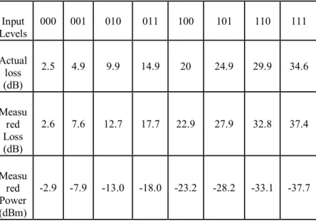
Table 2: Attenuation at different input levels of frequency 30 MHz with input signal level as -0.3 dBm
Input Levels 000 001 010 011 100 101 110 111 Actual loss (dB) 2.5 4.9 9.9 14.9 20 24.9 29.9 34.6 Measu red Loss (dB) 2.6 7.6 12.7 17.7 22.9 27.9 32.8 37.4 Measu red Power (dBm) -2.9 -7.9 -13.0 -18.0 -23.2 -28.2 -33.1 -37.7
The table above shows the attenuation at different input levels at frequency of 30 MHz. having input signal level as -0.3 dBm with RF level at 0 dBm. Measured power is calculated by taking the difference of input signal level with that of measured loss.
The figure drawn below shows the graph between thru loss and TTL input levels. It is showing the step attenuation at 8 different TTL levels. The graph shows the difference between the measured loss and the actual loss due to insertion loss of the signal. Insertion is basically a thru loss calculated at TTL input level “000”.
Fig.3: Graph showing relation between Thru Loss and TTL input levels for 30 MHz
The graph has shown in figure 4 shows the relation between input voltage and the output channel counts. Based on the algorithm designed for AGC, the channel counts magnitude is compared with the threshold level and the channel output counts will remain in a band. Whenever the output channel counts reduces below the threshold, the 1 step attenuation is provided to keep it above the threshold level
Fig.4: Graph between input voltage v/s channel counts IV. CONCLUSION
Design and development of AGC block and communication interface for digital BPM has been developed. A prototype of digitally controlled Attenuator circuit is developed for testing the automatic gain controller software. Maximum attenuation at (1, 1, 1) of 35 dB has been observed. Attenuation for various other frequencies has been observed. For the operation of AGC, a complete algorithm has been designed and tested, in which whenever the signal amplitude falls below the threshold value, 1 step attenuation (5dB) is provided. Thus AGC has been tested and its results were analyzed.
References
[1] R. F. Lyon. "Automatic Gain Control in Cochlear Mechanics” in P. Dallos et al., The Mechanics and Biophysics of Hearing. Verlag. pp. 395–400, Springer-1990
[2] Automatic gain control in receivers by IulianRosu, VA3IUL, 2004.
[3] TOAT – 51020+, Digital Step Attenuator, Mini-circuits. [4] J.Hasi, C.J. Kenney, “Active beam attenuators for
synchrotron radiation”, IEEE nuclear science symposium and medical imaging conference record, 2012.
0 20000000 40000000 60000000 80000000 -40 -30 -20 -10 0 O /p C o unt s I/p voltage (dBm)
I/p voltage (dBm) vs O/P counts
2330 ISSN: 2278 – 7798 All Rights Reserved © 2014 IJSETR
[5] Banta, E., “Analysis of an automatic gain control(AGC)”, IEEE transactions on (volume: 9, issue: 2), 2003.
[6] Y. H. Chen, “A New Implementation of Beam Forming Network with RF Digital Step Attenuators for Measuring mobile WiMAX Phase Array Antenna Pattern” IEEE,International Instrumentation and Measurement Technology Conference Victoria, Vancouver Island, Canada, 2008.
[7] Anton Widarta and Tomoteru Kawakami, “A Simple RF Attenuation Measurement Technique with a Small Mismatch Uncertainty” IEEE TRANSACTIONS ON INSTRUMENTATION AND MEASUREMENT, VOL. 58, NO. 4, APRIL 2009.
[8] Ahmed Youssef and James Haslett, “Digitally-Controlled RF Passive Attenuator in 65 nm CMOS for Mobile TV Tuner ICs”, 2012
[9] RF technology and sciences by Ian Poole, Radio – electronics.com.
[10] Digital Step Attenuator offers precision and linearity by Minicircuits.
First Author:
Ms. Disha Singh, M. Tech Student (4th Sem.) from Gyan
Ganga Institute of Technology and Sciences, Jabalpur (M.P.). She has published 1 research paper in international journal.
Second Author:
Mr. Mohammed Arif, Asst. Professor in Gyan Ganga Institute of Technology and Sciences, Jabalpur (M.P.). I have published 8 research papers in various national and international journals and conferences. Out of this 8, one is from IEEE conference.
![Table 1: Specifications for Digital Step Attenuator (TOAT-51020+) [3]:](https://thumb-us.123doks.com/thumbv2/123dok_us/8222781.2180019/3.893.53.424.101.804/table-specifications-digital-step-attenuator-toat.webp)