Roland Hayn∗
Aix-Marseille Univ., CNRS, IM2NP-UMR 7334, 13397 Marseille Cedex 20, France and
Leibniz Institute for Solid State and Materials Research IFW Dresden, Helmholtzstr. 20, 01069 Dresden, Germany Te Wei
Aix-Marseille Univ., CNRS, IM2NP-UMR 7334, 13397 Marseille Cedex 20, France Vyacheslav M. Silkin
Donostia International Physics Center (DIPC), 20018 San Sebasti´an/Donostia, Basque Country, Spain Departamento de Pol´ımeros y Materiales Avanzados: F´ısica, Qu´ımica y Tecnolog´ıa,
Facultad de Ciencias Qu´ımicas, Universidad del Pa´ıs Vasco UPV/EHU, 20080 San Sebasti´an/Donostia, Basque Country, Spain and
IKERBASQUE, Basque Foundation for Science, 48013 Bilbao, Basque Country, Spain Jeroen van den Brink
Leibniz Institute for Solid State and Materials Research IFW Dresden, Helmholtzstr. 20, 01069 Dresden, Germany and
Institut f¨ur Theoretische Physik and W¨urzburg-Dresden Cluster of Excellence ct.qmat, Technische Universit¨at Dresden, 01062 Dresden, Germany
(Dated: November 18, 2020)
We consider the plasmon excitations in anisotropic two-dimensional Dirac systems, be it either anisotropic graphene or surfaces of topological insulators. Generalizing the exact density-density response function one finds a plasmon dispersion that is anisotropic already at the lowest frequencies. Asymptotic expressions are obtained for the dispersion in this regime. We show that the plasmon properties of the complete material class of anisotropic Dirac systems are characterized by just two dimensionless material parameters. The strong anisotropy can be used to guide the plasmon modes, introducing new functionalities to the field of Dirac plasmonics.
I. INTRODUCTION
Graphene and topological insulators (TI) are two-dimensional (2D) Dirac systems1,2in the sense that they have a linear electron (and hole) dispersion and a Dirac point where the Fermi surface shrinks to zero. The pe-culiarities of relativistic electrons and the high Fermi ve-locity make them unique systems to study fundamental phenomena like spin-momentum locking and open many interesting applications in nano-electronics. Replacing the spin in TI by the pseudo-spin in graphene leads to a high formal analogy between both types of systems, be it that the number of Dirac cones that are present in the 2D Brioullin zone in one case is odd and in the other even. In the doped case, these Dirac systems allow for collective charge excitations – plasmons – that are different from both bulk and surface plasmons of ordinary metals. A pure 2D Dirac plasmon, like its 3D counterpart, has no direct coupling to light due to the momentum mismatch. However, such a coupling can be created by proper sur-face modification that break translation symmetry, for instance by grating or nano-structuration. This allows for interesting applications such as terahertz photodetec-tors, motivating the field of graphene plasmonics, or more in general, Dirac plasmonics.3–6
Here we concentrate on systems having an anisotropic Dirac cone in particular with a high factor of anisotropy
A=vx/vy between two extremal Fermi velocities in the
two perpendicular directions x and y. A large factor of A = 18 was for instance predicted for the topolog-ical surface states of the 3D TI HgS,7 but other TI’s can have large anisotropy factors as well.8 Experimen-tally anisotropic Dirac cones were detected recently by angle resolved photoemission in for instance Ru2Sn3,9 CaMnBi2,10 BaMnBi2, and BaZnBi2.11 In graphene the Dirac cone warping produces some anisotropy in the dis-persion of the 2D and acoustic plasmons.12–15 External strain can cause spatial anisotropy in graphene, but the expected changes in the plasmon anisotropy are rather small.16
Quite a considerable amount of theoretical work had been devoted to tilted Dirac cones which can be found inα-(BEDT-TTF)2I3 (BEDT-TTF=bis(ethylene-dithio)tetrathiafuva) under pressure,17 in some other ganic quasi-two-dimensional materials as well as in or-thorombic borophene.18 The analytical result for the imaginary part of the density-density response has been given in Ref. 19 and for the real part in Ref. 20. There, also a slight anisotropy was included. Plasmons of a tilted cone in a magnetic field were analyzed in Ref. 21. How-ever, the analytical formula of Ref. 20 was criticized in Ref. 22 and we will clarify that point here for any possible anisotropic Dirac system. We will not consider the effect of tilting, but rather only spatial anisotropy that lowers in-plane rotation symmetry which is the usual case for anisotropic TI’s and for this situation will provide
certain limiting cases. We are going to derive handy an-alytical formulas for the anisotropic plasmon dispersion of a general anisotropic Dirac system being characterized by just 2 dimensionless material parameters.
II. HAMILTONIAN AND CHARGE RESPONSE We are considering electrons confined to two dimen-sions with Coulomb interactions. The Hamiltonian of an anisotropic Dirac system is given by
H =X
k
εkc†k↑ck↓+ε∗kc †
k↓ck↑, (1)
wherec†/crepresent fermion creation/annihilation oper-ators, k the 2D wavevector and the energy is given in terms of the velocitiesvx/vy in x/y direction as
εk=vyky+ ivxkx=|εk|exp(iΦk). (2)
The Hamiltonian describes anisotropic topological insu-lators or graphene if one replaces spin by pseudo spin and adds valley and spin degeneracies. The plasmon disper-sion can then be obtained by calculating the dielectric function in random phase approximation (RPA). The di-electric function at 2D wave vectorqand energy transfer
ω is related with the charge susceptibility (or density-density response function)
χ(q, ω) =hhρq;ρ−qii (3) with ρq= X kσ c†kσck+qσ
being expressed via a retarded Green’s function. In RPA we obtain
χ(q, ω) = χ0(q, ω) 1−V(q)χ0(q, ω)
, (4)
whereχ0 is the electron-hole bubble (in graphical repre-sentation) and V(q) = e2/(2|q|ε
0εrel) is the Coulomb
interaction in the 2D system. Following the calcula-tion for the isotropic case23–25 we generalize it to the anisotropic situation. By diagonalizing (1) one finds two energy branches±|εk|=λ|εk|. The unitary transforma-tion
˜
ck±= (ck↑exp(−iφk/2)±ck↓exp(iφk/2))/ √
2
diagonalizes the Hamiltonian (1) and gives the zero-order susceptibility as: χ0(q, ω) = X λλ0 χλλ0 0 =gX kλλ0 Fλλ0(n kλ−nk+qλ0) ω+ i0++λ|ε k| −λ0|εk+q| ,
due to spin and valley degeneracy). Also,{λ, λ0} =±1 denote the two branches of the dispersion andnkλ is in
general the Fermi functionnkλ =f(λ|εk| −εF) of theλ
branch but we restrict ourselves here to zero temperature andεF is the Fermi energy. The form factor is
Fλλ0 = (1 +λλ0cos(Φk+q−Φk))/2.
We consider now a doped situation with a Fermi energy
εF lying in the positive branch λ= +1. Since the
neg-ative branch is completely filled, χ−−0 is zero. We are interested in the real part of χ0 to determine the plas-mon dispersion via the zero of the denominator of (4). As in the isotropic case, the plasmon dispersion is dominated byχ++0 which can be expressed as:
χ++0 =g Z Z εk<εF dkxdky 4π2 F++(|ε k+q| − |εk|) ω2−(|ε k+q| − |εk|)2 . (5)
After introducing vectors K and Q with Ki = kivi/v, Qi = qivi/v (i = {x, y}) and v2 = vxvy we can write
|εk|=v|K|and cast integral (5) into the same form as for the isotropic case
χ++0 =g Z Z |K|<εFv dKxdKy 4π2 F++v(|K+Q| − |K|) ω2−v2(|K+Q| −K|)2 . We also see that Φk+q−Φk equals the angle between
K+Q and K. Therefore, we can use forχ++0 at wave vector q in the anisotropic case the expression for the isotropic caseχ++0 ,isoat wave vectorQwhich is also true for the other contributionsχ+0−andχ−0+. We find finally
χ0(q, ω) =χiso0 (Q, ω), (6) where we have to use the Fermi velocity v = √vxvy in χiso
0 . The exact expression ofχiso0 in the isotropic case is well known,23,24 but it now depends onQ=|Q| instead ofq=|q|. The dependence on the angleαof the plasmon propagation, whereqx=qcosαandqy =qsinαcan be
cast into a directional factorD:
Q=qD , D= s Acos2α+sin 2 α A . (7)
Using the known expression for χiso
0 , we find the exact expression for the density-density response function in the anisotropic case. It can be expressed like
χ0(q, ω) =Cg(κ, ν) , C=
gεF
2πv2¯h2 , (8) in dependence on the dimensionless parameters
ν= ¯hω
εF
, κ= q
qF
D , (9)
where we introduce ¯h from now on with qF being an
averaged Fermi wave vector defined byεF = ¯hvqF, and
where g(κ, ν) =−1 +f G+ 2 +ν κ −G+ 2−ν κ
0.0 0.1 0.2 0.3 0.4 0.5 0.6
D * q/q
F 0.0 0.2 0.4 0.6 0.8 1.0 1.2 1.4 0/C
exact approx parabolicFIG. 1. Real part of the zero-order density-density response functionχ0/Cforν= ¯hω/εF = 0.6. Compared are the exact
expression (red, full line) with the approximative one (Eq. (10), blue dash-dotted line) and the parabolic approximation (Eq. (11), green dashed line).
and f = κ 2 8√ν2−κ2, G+(x) =x p x2−1−ln (x+px2+ 1).
This expression for the real part outside the continuum of electron-hole excitations whose border is given by ν=κ
and ν = 2−κ and where the imaginary part of χ0 is zero derives from the complete expression given in Refs. 23 and 24. The analytical expression (8) can also be obtained from the tilted case20,22by putting the tilt angle to zero in which case the difference between Refs. 20 and 22 disappears.
We are interested in the plasmon dispersion in the hy-drodynamic limitω→0 andq→0 where we can use the leading-order expression26:
g(κ, ν) = ν 2 √
ν2−κ2 −1. (10)
Forνκthat simplifies to
g(κ, ν) = κ 2
2ν2 . (11)
To illustrate the different approximations we present them in Fig. 1 together with the exact expression for
ν = 0.6. At small q all three expressions coincide, but
χ0 diverges if κ=Dq/qF approaches the continuum of
particle-hole excitations κ=ν which is not the case in the parabolic approximation in Eq. (11).
III. PLASMON
The plasmon dispersion is determined by solving
V(q)χ0(q, ω) = 1 which is in dimensionless form
q qF
= 2βg(κ, ν), (12)
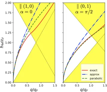
FIG. 2. Plasmon dispersion for material parametersβ= 2.0 andA= 1.5 for the two extremal plasmon propagation direc-tionsα= 0 (left) andα=π/2 (right) using the exact expres-sion or the two approximate ones (see Fig. 1) together with the corresponding boundaries of the continuum of electron-hole excitations (yellow) shown by dotted lines.
where we introduce the dimensionless material parameter
β= ge
2
8πε0εrel¯hv
. (13)
In the parabolic approximation for small q and ω the plasmon dispersion can be explicitly given,
¯ hω εF =pβ r q qF D , (14)
and is especially simple. The square-root dispersion is of course characteristic to 2D systems.
Any anisotropic Dirac system is characterized by the degeneracyg, the Fermi velocity v, the anisotropy A =
vx/vy, the relative dielectric constantεrel, and the Fermi
energy εF closely related with the filling of the Dirac
cone. The plasmon dispersion which is given by the solu-tion of (12) is valid for any anisotropic Dirac system and characterized by just two material parametersβ and A. At the same time, without tilting, the analytical result (12) is rather simple.
The exact plasmon dispersion together with that one resulting from the two approximations (10) and (11) is shown in Figs. 2 and 3 for two different sets of mate-rial parameters. In all cases, we show the two extremal directions α = 0 and α = π/2. The behavior is dif-ferent for materials with β larger than one and having a relatively small anisotropy (represented in Fig. 2 for
β = 2.0 and A = 1.5) from that one for β being con-siderably smaller than one and having a large anisotropy (Fig. 3 for β = 0.4 and A = 6.0). In Fig. 2 both ap-proximations represent relatively well the exact plasmon
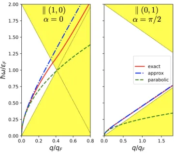
FIG. 3. Plasmon dispersion for material parametersβ= 0.4 and A = 6.0 for the two extremal plasmon propagation di-rections α = 0 (left) and α = π/2 (right) using the exact expression or the two approximate ones (see Figs. 1 and 2). The continuum of electron-hole excitations is indicated in yel-low.
dispersion. The square-root dispersion never crosses the line ν = κ and enters into the continuum of electron-hole excitations where it gets a final life-time by crossing the upper line ν = 2−κ. That is different in Fig. 3. There the square-root dispersion crosses the line ν =κ
which is especially visible forα=π/2 in the right hand part of the figure. Just relying on the parabolic approx-imation would imply that the plasmon becomes damped above a critical valueνc =β/
√
A which was incorrectly inferred in Ref. 26 for Bi2Se3. In effect, due to the diver-gence of χ0 atν =κ, the exact plasmon dispersion can never cross the lineν=κsuch that the plasmon remains undamped up to a criticalνc of order one. Lines of
con-stant plasmon energy are shown in Fig. 4 for β = 2.0 andA= 2.5. Clearly, they deviate strongly from simple ellipses which are expected for a tilted Dirac cone22 and show a remarkable anisotropy which increases at small plasmon energies.
IV. MATERIALS
The material parameterβ can vary quite considerably in different Dirac systems. For graphene with g = 4,
εrel = 2.4, and v = 9×10⁵ms−1, one finds β = 2.08,
exceedingβ= 1 considerably.
For Bi2Se3 a bulk dielectric constant perpendicular to thec-axis ofεrel≈27 was obtained in the first-principles
calculations.27Experimentally determinedεrel≈29 was
obtained using single crystals.28,29 Employing the latter value together withv= 5×10⁵ms−1 andg= 1 leads to
FIG. 4. Contour plot of the anisotropic plasmon dispersion with lines of constant plasmon energy in theqx-qy plane for
material parametersβ= 2.0 andA= 2.5.
β= 0.10, which compares well with the simulation of the measured plasmon dispersion in Ref. 30.
Turning to anisotropic Dirac systems we have to dis-tinguish two different cases, systems like HgS or Ag2Te with a preferred direction of plasmon propagation, or ma-terials of the BaMnBi2 class which preserve a fourfold rotation symmetry axis at the surface despite the strong anisotropy of the Dirac cones. Our theory directly applies to the first class of systems. The anisotropy factor was predicted to be 18 (HgS)7 or about 10 (Ag2Te)8. Theβ parameter is more difficult to estimate due to the uncer-tain knowledge aboutεrel. By comparison with Bi2Se3 theβ parameter can be assumed to be smaller or close to 1. So one expects a scenario close to that reported in Fig. 3, with an even higher anisotropy factorA.
For the other class of anisotropic Dirac cones with con-served 4 fold rotation symmetry, there are all together 4 anisotropic Dirac cones being pairwise perpendicular to each other. Therefore, one obtains four contributions to
χ0: χ0= gεF 4π Q 12 ω2 + Q22 ω2 , (15)
where the preferred direction of one cone Q12 =
q2(Acos2α+ sin2α/A) is perpendicular to that one of the other coneQ22=q2(Asin2α+ cos2α/A) andg= 2. We see that the anisotropy disappears in the leading or-der and remains only in higher oror-ders. The anisotropy is expected to be much smaller than in the other class of anisotropic TI’s and to appear only for larger values ofq
V. DISCUSSION AND CONCLUSIONS We have shown how the well-known square-root dis-persion for 2D Dirac plasmons can be generalized to the anisotropic case. Interestingly, the entire material class of anisotropic Dirac systems can be described by just two material parameters β and A. For materials with small values of β the square-root dispersion applies only for very small frequencies and has to be replaced by a more exact one close to the continuum of electron-hole exci-tations. Materials with high anisotropy factor A show strongly anisotropic plasmon excitations in the entire en-ergy range up to very small frequencies. Controlling ei-ther of the material parameters opens the pathway to engineer and customize 2D Dirac systems for plasmon-ics. In particular, for high anisotropies, plasmon wave guides may be constructed.31,32 It should be mentioned, that anisotropic low-energy plasmons can also be real-ized in other 2D systems with a non-linear band disper-sion like phosphorene,33–38 borophene,39–41and MoS
2.42 However, the amount of anisotropy is not so pronounced
there as we predict here.
Verifying the predicted anisotropy of the plasmon dispersion requires measurements at the surface of anisotropic TI’s. One interesting candidate system is Ag2Te for which the anisotropic Dirac cone was experi-mentally verified. A useful technique to measure the plas-mon dispersion at the surface of a TI is electron energy loss spectroscopy (EELS) in reflection geometry. Also optical measurements are possible that require periodic structure modifications, for instance surface grating.
Acknowledgements - R.H. thanks M. Knupfer, S.-L.
Drechsler, and M. Richter for very helpful discussions. V.M.S. acknowledges financial support from the Spanish Ministry Science and Innovation (Grant No. PID2019-105488GB-I00). J.v.d.B. acknowledges financial sup-port from the German Research Foundation (Deutsche Forschungsgemeinschaft, DFG) via SFB1143 Project No. A5 and under Germanys Excellence Strategy through the W¨urzburg-Dresden Cluster of Excellence on Complexity and Topology in Quantum Matter ct.qmat (EXC 2147, Project No. 390858490).
∗
1 A. K. Geim and K. S. Novoselov, Nature Mater. 6, 183
(2007).
2
C. L. Kane and E. J. Mele, Phys. Rev. Lett. 95, 146802 (2005).
3
A.N. Grigorenko, M. Polini, and K. S. Novoselov, Nature Photon.6, 749 (2012).
4 F. H. L. Koppens, D. E. Chang, and F. J. Garcia de Abajo,
Nano Lett.11, 3370 (2011).
5
P. Di Pietro, M. Ortolani, O. Limaj, A. Di Gaspare, V. Giliberti, F. Giorgianni, M. Brahlek, N. Bansal, N. Koirala, S. Oh, P. Calvani, and S. Lupi, Nat. Nanotechnol.
8, 556 (2013).
6
F. J. Garcia de Abajo, ACS Photonics1, 135 (2014).
7 F. Virot, R. Hayn, M. Richter, and J. van den Brink, Phys.
Rev. Lett.106, 236806 (2011).
8
W. Zhang, R. Yu, W. Feng, Y. Yao, H. Weng, X. Dai, and Z. Fang, Phys. Rev. Lett.106, 156808 (2011).
9
Q. D. Gibson, D. Evtushinsky, A. N. Yaresko, V. B. Zabolotnyy, M. N. Ali, M. K. Fuccillo, J. van den Brink, B. B¨uchner, R. J. Cava, and S. V. Borisenko, Sci. Rep.4, 5168 (2014).
10
Y. Feng, Z. J. Wang, C. Y. Chen, Y. G. Shi, Z. J. Xie, H. A. Yi, A. J. Liang, S. L. He, J. F. He, Y. Y. Peng, X. Liu, Y. Liu, L. Zhao, G. D. Liu, X. O. Dong, J. Zhang, C. T. Chen, Z. A. Xu, X. Dai, Z. Fang, and X. J. Zhou, Sci. Rep.
4, 5385 (2014).
11 H.Ryu, S.Y. Park, L.Li, W. Ren, J.B. Neaton, C. Petrovic,
C. Hwang, and S.-K. Mo, Sci. Rep.8, 15322 (2018).
12
A. Hill, S. A. Mikhailov, and K. Ziegler, EPL87, 27005 (2009).
13
Y. Gao and Z. Yuan, Solid State Commun. 151, 1009 (2011).
14 V. Despoja, D. Novko, K. Dekani´c, M. ˇSunji´c, and L.
Maruˇsi´c, Phys. Rev. B87, 075447 (2013).
15
M. Pisarra, A. Sindona, P. Riccardi, V. M. Silkin, and J.
M. Pitarke, New J. Phys.16, 083003 (2014).
16 S.-M. Choi, S.-H. Jhi, and Y.-W. Son, Phys. Rev. B81,
081407 (2010).
17
N. Tajima, S. Sugawara, M. Tamura, Y. Nishio, and K. Kajita, J. Phys. Soc. Jpn.75, 051010 (2006).
18
B. Feng, O. Sugino, R.-Y. Liu, J. Zhang, R. Yukawa, M. Kawamura, T. Iimori, H. Kim, Y. Hasegawa, H. Li, L. Chen, K. Wu, H. Kumigashira, F. Komori, T.-C. Chiang, S. Meng, and I. Matsuda, Phys. Rev. Lett. 118, 096401 (2017).
19
T. Nishine, A. Kobayashi, and Y. Suzumura, J. Phys. Soc. Jpn.79, 114715 (2010).
20
K. Sadhukhan and A. Agarwal, Phys. Rev. B 96, 035410 (2017).
21 J. S´ari, C. T¨oke, and M.O. Goerbig, Phys. Rev. B 90,
155446 (2014).
22
Z. Jalali-Mola and S. A. Jafari, Phys. Rev. B 98, 195415 (2018).
23
B. Wunsch, T. Stauber, F. Sols, and F. Guinea, New J. Phys.8, 318 (2006).
24 E. H. Hwang and S. Das Sarma, Phys. Rev. B75, 205418
(2007).
25
A. Principi, M. Polini, and G. Vignale, Phys. Rev. B80, 075418 (2009).
26 S. Raghu, S. B. Chung, X.-L. Qi, and S.-C. Zhang, Phys.
Rev. Lett.104, 116401 (2010).
27
I. A. Nechaev, R. C. Hatch, M. Bianchi, D. Guan, C. Friedrich, I. Aguilera, J. L. Mi, B. B. Iversen, S. Bl¨ugel, Ph. Hofmann, and E. V. Chulkov, Phys. Rev. B87, 121111 (2013).
28 W. Richter, H. K¨ohler, and C. R. Becker, Phys. Stat. Sol.
(b)84, 619 (1977).
29
M. Stordeur, K. K. Ketavonc, A. Priemuth, H. Sobotta, and V. Riede, Phys. Stat. Sol. (b)169, 505 (1992).
30 A. Politano, V. M. Silkin, I. A. Nechaev, M. S. Vitiello,
216802 (2015).
31 W.-L. Ma, P. Alonso-Gonz´alez, S.-J. Li, A. Y. Nikitin,
J. Yuan, J. Mart´ın-S´anchez, J. Taboada-Guti´errez, I. Amenabar, P.-N. Li, S. V´elez, C. Tollan, Z.-G. Dai, Y.-P. Zhang, S. Sriram, K. Kalantar-Zadeh, S.-T. Lee, R. Hil-lenbrand, and Q.-L. Bao, Nature562, 557 (2018).
32
W.-L. Ma, B. Shabbir, Q.-D. Ou, Y.-M. Dong, H.-Y. Chen, P.-N. Li, X.-L. Zhang, Y.-R. Lu, and Q.-L. Bao, InfoMat.
2, 777 (2020).
33
T. Low, R. Rold´an, H. Wang, F. Xia, P. Avouris, L. M. Moreno, and F. Guinea, Phys. Rev. Lett. 113, 106802 (2014).
34
R.-T. Lam and J. Guo, J. Appl. Phys.117, 113105 (2015).
35 B. Ghosh, P. Kumar, A. Thakur, Y. S. Chauhan, S.
Bhowmick, and A. Agarwal, Phys. Rev. B 96, 035422
36 S. Saberi-Pouya, T. Vazifehshenas, T. Salavati-fard, and
M. Farmanbar, Phys. Rev. B96, 115402 (2017).
37
I.-H. Lee, L. Martin-Moreno, D. A. Mohr, K. Khaliji, T. Low, and S.-H. Oh, ACS Photonics5, 2208 (2018).
38 C. Wang, G. W. Zhang, S. Y. Huang, Y. G. Xie, and H.
Yan, Adv. Opt. Mater.8, 1900996 (2020).
39
C. Lian, S.-Q. Hu, J. Zhang, C. Cheng, Z. Yuan, S. Gao, and S. Meng, Phys. Rev. Lett.125, 116802 (2020).
40
S. A. Dereshgi, Z. Z. Liu, and K. Aydin, Opt. Exp. 28, 16725 (2020).
41 Y. Huang, S. N. Shikodkar, and B. I. Yakobson, J. Amer.
Chem. Soc.139, 17181 (2017).
42
Z. Torbatian and R. Asgari, J. Phys.: Condens. Matter29, 465701 (2017).