© Copyright 2010–2012 Xilinx, Inc. Xilinx, the Xilinx logo, Artix, ISE, Kintex, Spartan, Virtex, Zynq, and other designated brands included herein are trademarks of
Introduction
The LogiCORE™ IP AXI Interconnect core connects one or more AXI memory-mapped master devices to one or more memory-mapped slave devices. The AXI interfaces conform to the AMBA® AXI version 4 specification from ARM®, including the AXI4-Lite control register interface subset.
Note: The AXI Interconnect core is intended for
memory-mapped transfers only; AXI4-Stream transfers are not applicable. IP with AXI4-Stream interfaces are generally connected to one another, and to DMA IP.
The AXI Interconnect core is provided as a non-encrypted, non-licensed (free) processor core (pcore) in the Xilinx® Platform Studio (XPS) software. The core is also provided in the ISE® Design Suite for use in non-embedded designs via the CORE Generator™ tool flow.
Features
The XPS tool flow provides access to all features of the AXI Interconnect core. The CORE Generator tool flow provides access to a subset of these features, as described in this section.
XPS Supported Features
These features of the AXI Interconnect core are supported by the XPS tool flow:
• AXI protocol compliant (AXI3, AXI4, and AXI4-Lite), and includes:
• Burst lengths up to 256 for incremental (INCR) bursts
• Converts AXI4 bursts > 16 beats when targeting AXI3 slave devices by splitting transactions
• Generates REGION outputs for use by slave devices with multiple address decode ranges • Propagates USER signals on each channel, if
any; independent USER signal width per channel (optional)
• Propagates Quality of Service (QoS) signals, if any; not used by the AXI Interconnect core (optional)
• Interface data widths:
• AXI4: 32, 64, 128, 256, 512, or 1024 bits • AXI4-Lite: 32 bits
• 32-bit address width
DS768 December 18, 2012 Product Specification
LogiCORE IP Facts Table Core Specifics
Supported
Device Family(1)
1. For a complete list of supported derivative devices, see IDS Embedded Edition Derivative Device Support.
Zynq™-7000, Artix™-7, Virtex®-7, Kintex™-7,
Virtex-6, Spartan®-6
Supported User
Interfaces AXI4, AXI4-Lite, AXI3
Resources Frequency
Configuration LUTs FFs SlicesDSP RAMsBlock Max. Freq.
Config1 N/A N/A N/A N/A N/A
Provided with Core
Documentation Product Specification
Design Files Verilog, VHDL
Example Design Figure 1, page 7
Test Bench Not Provided
Constraints File User Constraints File (UCF)
Simulation
Model Not Provided
Supported S/W
Driver N/A
Tested Design Tools
Design Entry
Tools ISE Design Suite v14.4, PlanAhead™ tool, XPS
Simulation(2)
2. For the supported versions of the tools, see the ISE Design Suite 14: Release Notes Guide.
Mentor Graphics ModelSim, Cadence Incisive Enterprise Simulator (IES)
Synthesis Tools XST v14.4
Support
XPS Supported Features (
Continued
)
• The Slave Interface (SI) of the core can be configured to comprise 1-16 SI slots to accept transactions from up to 16 connected master devices. The Master Interface (MI) can be configured to comprise 1-16 MI slots to issue transactions to up to 16 connected slave devices.
• When connecting one master to one slave, the AXI Interconnect core can optionally perform address range checking. It can also perform any of the optional data-width conversions, clock-rate conversions, protocol conversions, register pipelining, and datapath buffering functions.
• When connecting one master to one slave, and not performing any conversions or address range checking, the AXI Interconnect core is implemented as wires, with no resources, no delay, and no latency.
Built-in data-width conversion:
• Each master and slave connection can independently use data widths of 32, 64, 128, 256, 512, or 1024 bits wide:
- The internal crossbar can be configured to have a native data width of 32, 64, 128, 256, 512, or 1024 bits. - Data-width conversion is performed for each master and slave connection that does not match the
crossbar native data width.
• When converting to a wider interface (upsizing), data is packed (merged) when permitted by address channel control signals (CACHE modifiable bit is asserted).
• When converting to a narrower interface (downsizing), burst transactions are split into multiple transactions if the maximum burst length would otherwise be exceeded.
Built-in clock-rate conversion:
• Each master and slave connection can use independent clock rates.
• Synchronous integer-ratio (N:1 and 1:N) conversion to the internal crossbar native clock rate. • Asynchronous clock conversion (uses more storage and incurs more latency than synchronous
conversion).
• The AXI Interconnect core exports reset signals resynchronized to the clock input associated with each SI and MI slot.
Built-in AXI4-Lite protocol conversion:
• The AXI Interconnect core can connect to any mixture of AXI4 and AXI4-Lite masters and slaves. • The AXI Interconnect core saves transaction IDs and restores them during response transfers, when
connected to an AXI4-Lite slave.
- AXI4-Lite slave devices do not need to sample or store IDs.
• The AXI Interconnect core detects illegal AXI4-Lite transactions from connected AXI4 masters, such as any transaction that results in a burst of more than one word. The AXI Interconnect core generates a
protocol-compliant error response to the connected master, and does not propagate the illegal transaction to the AXI4-Lite slave device.
- The AXI4-Lite protocol conversion does not convert AXI4/AXI3 bursts into a sequence of single-beat transactions for AXI4-Lite slaves, so as to minimize resource utilization of the AXI4-Lite solution. • Write and Read transactions are single-threaded to AXI4-Lite slave devices, propagating only a single
address at a time, which typically nullifies the resource overhead of separate AXI write and read address signals.
Built-in AXI3 protocol conversion:
• The AXI Interconnect core splits burst transactions of more than 16 beats from connected AXI4 masters into multiple transactions of no more than 16 beats when connected to an AXI3 slave device.
Optional register-slice pipelining:
• Facilitates timing closure by trading-off frequency vs. latency.
• One latency cycle per register-slice, with no loss in data throughput under all AXI handshake conditions.
Optional datapath FIFO buffering:
• Available on Write and Read datapaths connecting to each master and each slave. • 32-deep LUT-RAM based.
• 512-deep block RAM based.
Selectable Interconnect Architecture:
• Crossbar mode (Performance optimized):
- Shared-Address, Multiple-Data (SAMD) crossbar architecture.
- Parallel crossbar pathways for Write data and Read data channels. When more than one Write or Read data source has data to send to different destinations, data transfers can occur independently and concurrently, provided AXI ordering rules are met.
- Sparse crossbar datapaths according to configured connectivity map, resulting in reduced resource utilization.
- One shared Write address arbiter, plus one shared Read address arbiter. Arbitration latencies typically do not impact data throughput when transactions average at least three data beats.
• Shared Access mode (Area optimized):
- Shared write data, shared read data, and single shared address pathways. - Issues one outstanding transaction at a time.
- Minimizes resource utilization.
Supports multiple outstanding transactions (crossbar mode):
• Supports connected masters with multiple reordering depth (ID threads). • Supports up to 16 bit wide ID signals (system-wide).
• Supports write response re-ordering. Read data re-ordering, and Read Data interleaving • Configurable Write and Read transaction acceptance limits for each connected master. • Configurable Write and Read transaction issuing limits for each connected slave.
• Optional single-thread mode (per connected master) reduces thread control logic by allowing one or more outstanding transactions from only one thread ID at a time.
“Single-Slave per ID” method of cyclic dependency (deadlock) avoidance:
• For each ID thread issued by a connected master, the Interconnect allows one or more outstanding transactions to only one slave device for Writes and one slave device for Reads, at a time.
Fixed priority and round-robin arbitration: • 16 configurable levels of static priority.
• Round-robin arbitration is used among all connected masters configured with the lowest priority setting (priority 0), when no higher priority master is requesting.
• Any SI slot that has reached its acceptance limit, or is targeting an MI slot that has reached its issuing limit, or is trying to access an MI slot in a manner that risks deadlock, is temporarily disqualified from
arbitration, so that other SI slots can be granted arbitration.
Supports TrustZone security for each connected slave as a whole:
- If configured as a secure slave device, only secure AXI accesses are permitted.
- Any non-secure accesses are blocked and the AXI Interconnect core returns a DECERR response to the connected master.
CORE Generator Tool Supported Features
These features of the AXI Interconnect core are supported by the CORE Generator tool flow: • AXI protocol compliant (AXI4 only), including:
• Burst lengths up to 256 for incremental (INCR) bursts
• Propagates Quality of Service (QoS) signals, if any; not used by the AXI Interconnect core (optional) • Interface data widths:
• 32, 64, 128, 256, 512, or 1024 bits • Address width: 12 to 64 bits
• Up to 16 Slave interfaces (to accept transactions from up to 16 connected master devices) and one Master Interface (to issue transactions to one connected slave device).
• When connecting one master to one slave, the AXI Interconnect core can optionally perform any of the optional data-width conversions, clock-rate conversions, register pipelining, and datapath buffering functions.
Built-in data-width conversion:
• Each master and slave connection can independently use data widths of 32, 64, 128, 256, 512, or 1024 bits: - The internal crossbar can be configured to have a native data width of 32, 64, 128, 256, 512, or 1024 bits. - Data-width conversion is performed for each master and slave connection that does not match the
crossbar native data width.
• When converting to a wider interface (upsizing), data is packed (merged) when permitted by address channel control signals (CACHE modifiable bit is asserted).
• When converting to a narrower interface (downsizing), burst transactions are split into multiple transactions if the maximum burst length otherwise would be exceeded.
Built-in clock-rate conversion:
• Each master and slave connection can use independent clock rates.
• Synchronous integer-ratio (N:1 and 1:N) conversion to the internal crossbar native clock rate. • Asynchronous clock conversion (uses more storage and incurs more latency than synchronous
conversion).
• The AXI Interconnect core exports reset signals resynchronized to the clock rate of each connected master and slave.
Optional register-slice pipelining:
• Available on all AXI channels connecting to each master and slave device. • Facilitates timing closure by trading-off frequency vs. latency.
• One latency cycle per register-slice, with no loss in data throughput under all AXI handshake conditions.
Optional datapath FIFO buffering:
• Available on Write and Read datapaths connecting to each master and each slave. • 32-deep LUT-RAM based.
• 512-deep block RAM based.
• Optional packet FIFO operation to avoid full/empty stalls in the middle of bursts.
Supports multiple outstanding transactions:
• Supports connected masters with multiple reordering depth (ID threads).
• Supports up to 8 bit wide ID signals from each connected master device (produces up to 12 bit wide ID output).
• Supports write response re-ordering. Read data re-ordering, and Read Data interleaving • Configurable Write and Read transaction acceptance limits for each connected master. • Configurable Write and Read transaction issuing limits for connected slave.
Fixed priority and round-robin arbitration: • 16 configurable levels of static priority.
• Round-robin arbitration is used among all connected masters configured with the lowest priority setting (priority 0), when no higher priority master is requesting.
• Any master device that has reached its acceptance limit is temporarily disqualified from arbitration, so that other connected masters can be granted arbitration.
Support for Read-only and Write-only master devices, resulting in reduced resource utilization.
Summary of CORE Generator Tool Flow Limitations
With respect to the features described in this document, the CORE Generator tool flow has these limitations: • The process of defining an address map and all features relating to address decoding and selecting among
multiple target slave devices is reserved for the XPS flow at this time. When used in the CORE Generator tool flow, the Interconnect supports connecting to only one slave device, and all transaction addresses are simply propagated. There are no conditions that result in the Interconnect producing a decode error (DECERR) response when used in the CORE Generator tool flow.
• Only AXI4 (memory-mapped) protocol is supported. When used in the CORE Generator tool flow, the Interconnect is intended only to connect to memory-type slave devices, such as an external memory controller, and not to control-register (AXI4-Lite) slaves.
• USER signals are not supported.
• Register slices are selectable per interface and apply to all AXI channels when enabled. The register slice type used per channel is fixed: Fully registered for W and R channels, Light weight for AW, AR, and B channels. • Only full crossbar mode is supported, providing independent write and read operations for both address and
data transfers. The “Shared Access” mode is not supported. Sparse crossbar connectivity is not applicable, as there is only one connected slave device.
• The width of ID signals is selected globally and applies to all Slave Interface (SI) ports. The Interconnect always adds four high-order bits when issuing the Master Interface ID signals, which indicate the originating SI index number.
• TrustZone security is not provided as a service of the Interconnect. (AW/ARPROT signals are propagated to the slave device.)
AXI Interconnect Core Limitations
These limitations apply to the AXI Interconnect core as a whole (both the XPS and CORE Generator tool flows):
The AXI Interconnect core does not support these AXI3 features:
- Atomic locked transactions. This feature was retracted by AXI4 protocol. A locked transaction is changed to a non-locked transaction and propagated by the MI.
- Write interleaving. This feature was retracted by AXI4 protocol. AXI3 master devices must be configured as if connected to a slave with Write interleaving depth of one.
AXI4 QoS signals do not influence arbitration priority. QoS signals are propagated from SI to MI.
The AXI Interconnect core does not convert multi-beat bursts into multiple single-beat transactions when targeting an AXI4-Lite slave device.
The AXI Interconnect core does not time-out if the destination of any AXI channel transfer stalls indefinitely. All connected AXI slaves must respond to all received transactions, as required by AXI protocol.
The AXI Interconnect core provides no address remapping.
The AXI Interconnect core provides no built-in conversion to non-AXI protocols, such as APB.
The AXI Interconnect core does not have clock-enable (ACLKEN) inputs. Consequently, the use of ACLKEN is not supported among memory-mapped AXI interfaces in Xilinx systems.
Note: The ACLKEN signal is supported for Xilinx AXI4-Stream interfaces.
Definitions, Acronyms, and Abbreviations
Table 1 provides a list of acronyms, abbreviations, and specific definitions used in this document.
Table 1: Definitions, Acronyms, and Abbreviations
Item Description
AXI The generic term for all implemented AXI protocol interfaces. master device or
connected master
An IP or device (or one of multiple interfaces on an IP) that generates AXI transactions out from the IP onto the wires connecting to a slave IP.
slave device or connected slave
An IP or device (or one of multiple interfaces on an IP) that receives and responds to AXI transactions coming in to the IP from the wires connecting to a master IP.
master interface (generic)
An interface of an IP or module that generates out-bound AXI transactions and thus is the initiator (source) of an AXI transfer. On AXI master interfaces, AWVALID, ARVALID, and WVALID are outputs, and RVALID and BVALID are inputs.
slave interface (generic)
An interface of an IP or module that receives in-bound AXI transactions and becomes the target (destination) of an AXI transfer. On AXI slave interfaces, AWVALID, ARVALID, and WVALID are inputs, and RVALID and BVALID are outputs.
SI AXI Interconnect Slave Interface: For XPS flow, Vectored AXI slave interface receiving in-bound AXI transactions from all connected master devices. For CORE Generator tool flow, one of multiple slave interfaces connecting to one master device.
MI AXI Interconnect Master Interface: For XPS flow, Vectored AXI master interface generating out-bound AXI transactions to all connected slave devices. For CORE Generator tool flow, one master interface connecting to one slave device.
SI slot Slave Interface Slot: A slice of the Slave Interface vector signals of the AXI Interconnect core that connect to a single master device.
MI slot Master Interface Slot: A slice of the Master Interface vector signals of the AXI Interconnect core that connect to a single slave device.
SI-side A module interface closer to the SI side of the AXI Interconnect core. MI-side A module interface closer to the MI side of the AXI Interconnect core.
Crossbar Module at the center of the AXI Interconnect core that routes address, data and response channel transfers between various SI slots and MI slots.
SI hemisphere Conversion and storage modules of the AXI Interconnect core located between the SI and crossbar. MI hemisphere Conversion and storage modules of the AXI Interconnect core located between the crossbar and MI. upsizer Data width conversion function in which the datapath width gets wider when moving in the direction from
the SI-side toward the MI-side (regardless of write/read direction).
downsizer Data width conversion function in which the datapath width gets narrower when moving in the direction from the SI-side toward the MI-side (regardless of write/read direction).
Functional Description
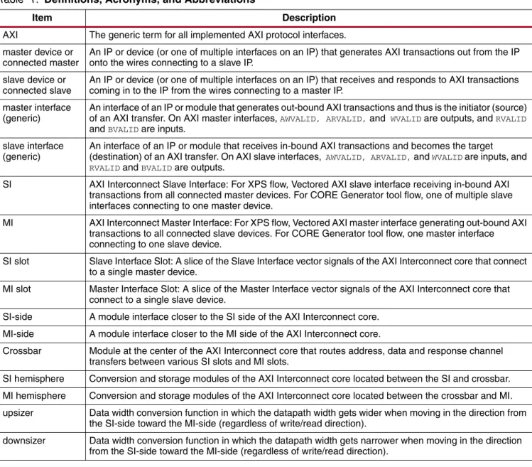
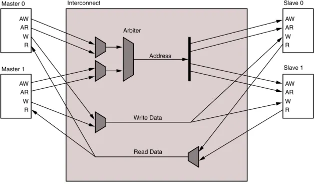
Figure 1 shows the top-most AXI Interconnect core block diagram.
The AXI Interconnect core consists of the SI, the MI, and the functional units that comprise the AXI channel pathways between them. The SI accepts Write and Read transaction requests from connected master devices. The MI issues transactions to slave devices. At the center is the crossbar that routes traffic on all the AXI channels between the various devices connected to the SI and MI. The AXI Interconnect core also comprises other functional units located between the crossbar and each of the interfaces that perform various conversion and storage functions. The crossbar effectively splits the AXI Interconnect core down the middle between the SI-related functional units (SI hemisphere) and the MI-related units (MI hemisphere).
The following subsection describes the use models for the AXI Interconnect core.
Use Models
The AXI Interconnect core connects one or more AXI memory-mapped master devices to one or more memory-mapped slave devices. These use cases are described:
• Pass Through
• Conversion Only
• N-to-1 Interconnect
• 1-to-N Interconnect
• N-to-M Interconnect (Crossbar Mode)
• N-to-M Interconnect (Shared Access Mode)
X-Ref Target - Figure 1
Figure 1: AXI Interconnect Core Diagram
AXI Interconnect
Slave Interface
Master Interface
SI Hemisphere MI Hemisphere
Crossbar Master 0 Slave 0 Slave 1 Master 1 Regi s ter S lice s Regi s ter S lice s Up-s iz er s Up-s iz er s Cloc k Con v e rter s Do wn-s iz er s D a t a FIFO s Cloc k Con v e rter s Do wn-s iz er s Protocol Con v e rter s D a t a FIFO s X12047
Pass Through
When there is only one master device and only one slave device connected to the AXI Interconnect core, and the AXI Interconnect core is not performing any optional conversion functions or pipelining, all pathways between the slave and master interfaces degenerate into direct wire connections with no latency and consuming no logic resources. Figure 2 shows the Pass Through diagram. The AXI Interconnect core does, however, continue to resynchronize the INTERCONNECT_ARESETN input to each of the slave and master interface clock domains for any master or slave devices that connect to the ARESET_OUT_N outputs, which consumes a small number of flip-flops.
Conversion Only
The AXI Interconnect core can perform various conversion and pipelining functions when connecting one master device to one slave device. These conversion and pipelining functions are:
• Data width conversion • Clock rate conversion • AXI4-Lite slave adaptation • AXI-3 slave adaptation
• Pipelining, such as a register slice or data channel FIFO
In these cases, the AXI Interconnect core contains no arbitration, decoding, or routing logic (unless optional address range checking is enabled). There could be latency incurred, depending on the conversion being performed.
Figure 3 shows an example of a one-to-one conversion use case.
X-Ref Target - Figure 2
Figure 2: Pass-through AXI Interconnect Use Case
X-Ref Target - Figure 3
Figure 3: 1-to-1 Conversion AXI Interconnect Use Case
X12048 Master 0 Slave 0 Interconnect X12049 Master 0 Slave 0 Interconnect
Conver
s
ion
a
nd/or
Pipelining
N-to-1 Interconnect
A common degenerate configuration of the AXI Interconnect core occurs when multiple master devices arbitrate for access to a single slave device, typically a memory controller.
In these cases, address decoding logic might be unnecessary and omitted from the AXI Interconnect core (unless the optional address range validation is enabled). Any of the optional conversion functions, such as data width and clock rate conversion, can also be performed in this configuration as shown in Figure 4.
1-to-N Interconnect
Another degenerative configuration of the AXI Interconnect core occurs when a single master device, typically, a processor, accesses multiple memory-mapped slave peripherals. In these cases, arbitration (in the address and Write data paths) is not performed, as shown in Figure 5.
X-Ref Target - Figure 4
Figure 4: N-to-1 AXI Interconnect
X-Ref Target - Figure 5
Figure 5: 1-to-N AXI Interconnect Use Case
X12050 Master 0 Master 1 Slave 0 Interconnect Ar b iter X12051 Master 0 Slave 0 Slave 1 Interconnect Decoder/Ro u ter
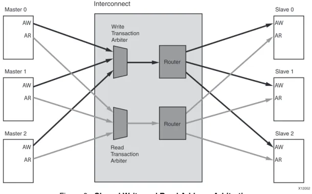
N-to-M Interconnect (Crossbar Mode)
The N-to-M use case of the AXI Interconnect core, when in Crossbar mode, features a Shared-Address Multiple-Data (SAMD) topology, consisting of sparse data crossbar connectivity, with single, shared Write and Read address arbitration, as shown in Figure 6 and Figure 7.
X-Ref Target - Figure 6
Figure 6: Shared Write and Read Address Arbitration
X-Ref Target - Figure 7
Figure 7: Sparse Crossbar Write and Read Data Pathways
X12052 Master 0 Master 1 Master 2 Slave 0 Slave 1 Slave 2 Interconnect AW AR AW AR AW AR AW AR AW AR AW AR Write Transaction Arbiter Read Transaction Arbiter Router Router X12053 Interconnect Master 0 Master 1 Master 2 Slave 0 Slave 1 Slave 2 W R W R W R W R W R W R
Write Data Crossbar
Parallel Write and Read data pathways connect each SI slot to all the MI slots that it can access, according to the configured sparse connectivity map. When more than one source has data to send to different destinations, data transfers can occur independently and concurrently, provided AXI ordering rules are met.
The Write address channels among all SI slots feed into a central address arbiter, which grants access to one SI slot at a time. It is also the case for the Read address channels.
The winner of each arbitration cycle transfers its address information to the targeted MI slot, and pushes an entry into the appropriate command queue(s) that enable various data pathways to route data to the proper destination while enforcing AXI ordering rules.
N-to-M Interconnect (Shared Access Mode)
When in Shared Access mode, the N-to-M use case of the AXI Interconnect core provides for only one outstanding transaction at a time, as shown in Figure 8. For each connected master, read transaction requests always take priority over writes. The arbiter then selects from among the requesting masters. A write or read data transfer is enabled to the targeted slave device. After the data transfer (including the write response) completes, the next request is arbitrated. Shared Access mode minimizes the resources used to implement the crossbar module of the Interconnect.
X-Ref Target - Figure 8
Figure 8: Shared Access Mode -ASTER -ASTER 3LAVE 3LAVE !7 !2 7 2 !7 !2 7 2 !7 !2 7 2 !7 !2 7 2 )NTERCONNECT !RBITER !DDRESS 7RITE$ATA 2EAD$ATA
AXI Interconnect Core Functionality
These subsections describe the functionality within the AXI Interconnect core.
• Top-Level Slave/Master Interface
• Width Conversion
• Width Conversion Transactions
• Clock Conversion
• Peripheral Register Slices
• Datapath FIFOs
• Use of ID Signals
• Multiple Address Range Support
• Cyclic Dependency Avoidance
• Error Signaling
Top-Level Slave/Master Interface
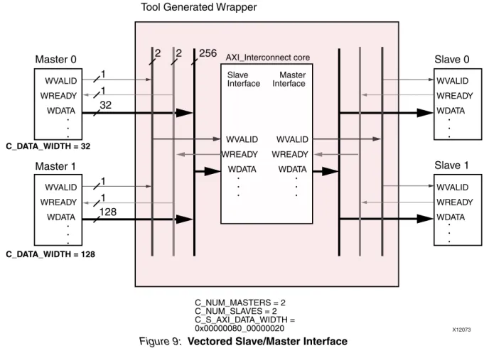
When deployed using the XPS flow, the top-level interface consists of a single, vectored AXI SI, plus a single, vectored AXI MI.
Each vectored interface can be configured to connect to between 1 and 16 master/slave devices.
For each signal comprising a vectored AXI interface on the core, its natural width is multiplied by the number of devices to which it is connected. All of the bit slices that connect to a single device are referred to as a slot of the interface. For example, the AWLEN signal carries an 8-bit value indicating the number of data beats in a Write transaction. If the AXI Interconnect core is configured with two SI slots, then the S_AXI_AWLEN signal is a total of 16 bits wide.
The effective widths of the WDATA, WSTRB, and RDATA signals are also configurable per MI/SI. The width of each of these signals on the vectored SI or MI is the maximum configured data width among all the SI and MI slots, as well as the Interconnect's native data width, multiplied by the number of slots. The unused high-order bits for each narrower slot are tied off (for inputs) or left unconnected (for outputs) within the AXI Interconnect core, and are trimmed by the implementation tools. Each AXI interface signal therefore allocates the same physical width across all slots.
For example, if the AXI Interconnect core is configured with two SI slots, one with data width 32 bits and one with data width 128 bits, and there are no larger data widths configured on any MI slot or the Interconnect itself, then each of the WDATA and RDATA signals on the SI of the core is a total of 256 bits wide, as shown in Figure 9.
Specifically:
• “slot 0” uses WDATA[31:0]
• “slot 1” uses WDATA[255:128], and connects to WDATA[127:0] of the “Master 1” device). • WDATA[127:32] remains tied off or unconnected inside the AXI Interconnect core.
Similar to I/O signals, many configuration parameters on the AXI Interconnect core are also formatted as vectors across all the SI or MI slots. Vectored parameters are formatted as follows:
• Parameters that define Boolean conditions, such as the TrustZone security indicator (C_M_AXI_SECURE), are formatted as bit vectors with one bit per slot.
• Parameters that define any numerical value, regardless of value range, are formatted as bit vectors with 32 bits per slot.
• Base and high addresses are an exception and are formatted as 64 bits per slot.
In the Figure 9 example, the value of the vectored parameter that defines the effective data widths of the slots on the SI (C_S_AXI_DATA_WIDTH) would be 0x0000008000000020, where 0x20 represents 32 bits for slot 0, and 0x80 represents 128 bits for slot 1. Parameter values are little-endian, as are I/O signals; consequently, the value corresponding to slot 0 appears at the right-hand Least Significant Bit (LSB) end of the parameter vector.
When deployed using the CORE Generator tool flow, an additional module layer is inserted above the vectored interface that splits up the vectored Slave Interface into individual enumerated interfaces suitable for direct connection to AXI master devices in an HDL design. This top-level module also splits out the individual SI-related parameters accordingly.
X-Ref Target - Figure 9
Figure 9: Vectored Slave/Master Interface
4OOL'ENERATED7RAPPER -ASTER 3LAVE 3LAVE -ASTER 76!,)$ 72%!$9 7$!4! 76!,)$ 72%!$9 7$!4! 76!,)$ 72%!$9 7$!4! 76!,)$ 72%!$9 7$!4! #?$!4!?7)$4( #?$!4!?7)$4( #?.5-?-!34%23 #?.5-?3,!6%3 #?3?!8)?$!4!?7)$4( X? !8)?)NTERCONNECTCORE 3LAVE
)NTERFACE )NTERFACE-ASTER
76!,)$ 72%!$9 7$!4! 76!,)$ 72%!$9 7$!4! 8
Width Conversion
The AXI Interconnect core has a parametrically defined, internal, native data width, which supports 32, 64, 128, 256, 512, or 1024 bits. The AXI data channels that span the crossbar are sized to the native width of the AXI Interconnect core, as specified by the C_INTERCONNECT_DATA_WIDTH parameter.
When any SI slots or MI slots are sized differently, the AXI Interconnect core inserts width conversion units to adapt the slot width to the AXI Interconnect native width before transiting the crossbar to the other hemisphere.
The width conversion functions differ depending on whether the datapath width gets wider (upsizing) or narrower (downsizing) when moving in the direction from the SI toward the MI. The width conversion functions are the same in either the SI hemisphere (translating from the SI to the AXI Interconnect native width) or the MI hemisphere (translating from the AXI Interconnect native width to the MI).
MI and SI slots have an associated individual parametric data width value. The AXI Interconnect core adapts each MI and SI slot automatically to the internal native data width as follows:
• When the data width of an SI slot is wider than the internal native data width of the AXI Interconnect core, a downsizing conversion is performed along the pathways of the SI slot.
• When the internal native data width of the AXI Interconnect core is wider than that of an MI slot, a downsizing conversion is performed along the pathways of the MI slot.
• When the data width of an SI slot is narrower than the internal native data width of the AXI Interconnect core, an upsizing conversion is performed along the pathways of the SI slot.
• When the internal native data width of the AXI Interconnect core is narrower than that of an MI slot, an upsizing conversion is performed along the pathways of the MI slot.
The following subsections describe downsizing and upsizing.
Downsizing
When the data width on the SI side is wider than that on the MI side, and the transfer size of the transaction is also wider than the data width on the MI side, then downsizing is performed and, in the transaction issued to the MI side, the number of data beats is multiplied accordingly.
• For writes, data serialization occurs • For reads, data merging occurs
The AXI Interconnect core sets the RRESP for each output data beat (on the SI) to the worst-case error condition encountered among the input data beats being merged, according to the following descending precedence order: DECERR, SLVERR, OKAY, EXOKAY.
When the transfer size of the transaction is equal to or less than the MI side data width, the transaction (address channel values) remains unchanged. Data transfers pass through unchanged except for byte-lane steering. This applies to both writes and reads.
When downsizing, the AXI Interconnect core factors up the length of each burst and detects when the resulting burst length would exceed the maximum burst limit (256 data beats for AXI4). In such cases, the AXI Interconnect core splits the transaction automatically into multiple conforming burst transactions.
• If the AWLOCK or ARLOCK signal indicates an Exclusive Access write or read transaction, and downsizing results in splitting, then the AXI Interconnect core changes the LOCK signal in all output transactions to indicate Normal Access (0).
• When a downsized Write transaction results in splitting, the AXI Interconnect core coalesces the multiple Write responses at the MI and issues one Write response on the SI. The core sets the error response code (BRESP) to the worst-case error condition encountered among the multiple input responses, according to the following descending precedence order: DECERR, SLVERR, OKAY (EXOKAY cannot occur in a split transaction).
Downsizing, including transaction splitting, is not restricted by values of the AW/ARCACHE signal (specifically the “modifiable” bit). Transaction splitting due to downsizing cannot be restricted by CACHE because there is no other alternative for completing the transaction. See Table 2, page 17 for the various size conversions.
The downsizer module allows multiple outstanding transactions to be propagated. Transaction characteristics from the AW/AR channel transfers are queued while awaiting corresponding response transfers. However, due to the possibility of write response and read data re-ordering, transaction acceptance by the AW and AR channel downsizers is restricted to a single ID thread at a time.
The interconnect does not support downsizing directly from 1024 bits to 32 bits, either between the SI and crossbar or between the crossbar and MI. If any SI is 1024 bits, then C_INTERCONNECT_DATA_WIDTH must be set to a value greater than 32. If the MI is 32 bits, then C_INTERCONNECT_DATA_WIDTH must be set to a value less than 1024.
Upsizing
When the data width on the MI side is wider than that on the SI side, then upsizing is performed. Data packing is performed (for INCR and WRAP bursts), provided the AW/ARCACHE[1] bit (“Modifiable”) is asserted.
In the resulting transaction issued to the MI side, the number of data beats is reduced accordingly. • For Writes, data merging occurs.
• For Reads, data serialization occurs.
• The AXI Interconnect core replicates the RRESP from each input data beat onto the RRESP of each output data beat (on the SI).
When the AW/ARCACHE[1] bit is deasserted, the transaction (address channel values) remains unchanged and data transfers pass through unchanged except for byte-lane steering.
This latter functionality is commonly referred to as an “expander.”
Upsizing never results in transaction splitting. See Table 2 for the various size conversions.
The upsizer module allows multiple outstanding transactions to be propagated. Transaction characteristics from the AW/AR channel transfers are queued while awaiting corresponding response transfers. However, due to the possibility of read data re-ordering, transaction acceptance by the AR-channel upsizer is restricted to a single ID thread at a time. Write transactions, however, are not restricted by ID thread, as B-channel responses require no transformation by the upsizer, and can therefore be propagated in any order as received.
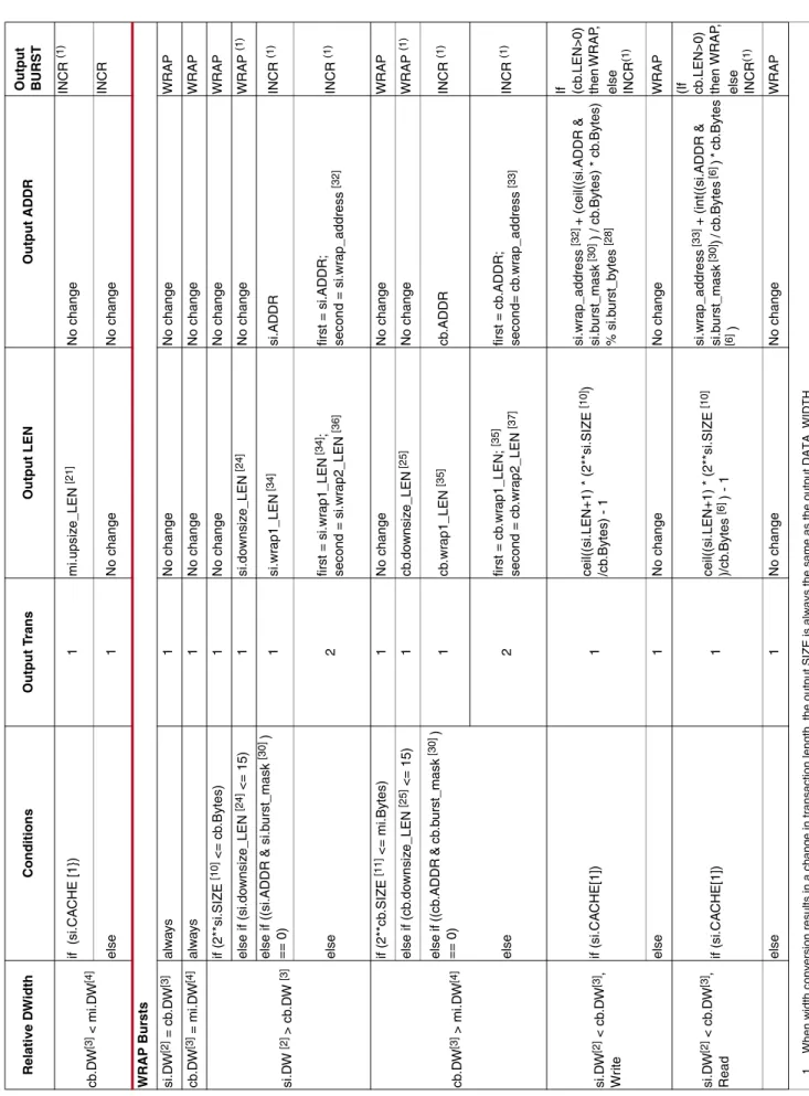
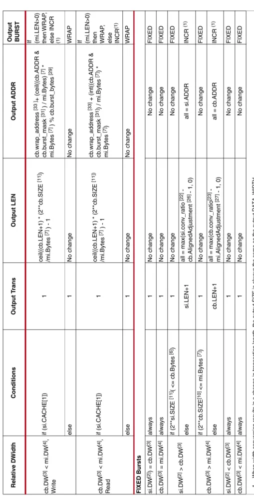
WIDTH Conversion Transaction Transformations
Table 2 uses these following designators when describing properties, signals, and derived equations:
• si = Slave Interface
• cb = Interconnect (crossbar) core • mi = Master Interface
Table 2 lists:
• SI hemisphere transformations when relative DWidth compares si.DW to cb.DW • MI hemisphere transformations when relative DWidth compares cb.DW to mi.DW
Supporting Equations
These width conversion equations are enumerated in Table 2.
1. When width conversion results in a change in transaction length, the output SIZE is always the same as the output DATA_WIDTH.
2. si.DW = C_S_AXI_DATA_WIDTH 3. cb.DW = C_INTERCONNECT_DATA_WIDTH 4. mi.DW = C_M_AXI_DATA_WIDTH 5. si.Bytes = si.DW[2] / 8 6. cb.Bytes = cb.DW[3] / 8 7. mi.Bytes = mi.DW[4] / 8 8. cb.ByteMask = cb.Bytes[5] - 1 9. mi.ByteMask = mi.Bytes[6] – 1
10. si.SIZE = S_AXI_AWSIZE or S_AXI_ARSIZE, as applicable 11. cb.SIZE = si.SIZE if (cb.LEN=si.LEN), else log2(cb.Bytes[6]) 12. mi.SIZE = cb.SIZE if (mi.LEN=cb.LEN), else log2(mi.Bytes[7]) 13. si.SizeMask = (2**si.SIZE[10]) – 1
14. cb.SizeMask = (2**cb.SIZE[11]) - 1 15. mi.SizeMask = (2**mi.SIZE[12]) – 1
16. cb.AlignedStart = si.ADDR & ~cb.ByteMask[8]
17. cb.AlignedEnd = ((si.ADDR & ~si.SizeMask[13]) + (si.LEN * 2**si.SIZE[10])) & ~cb.ByteMask[9] 18. cb.upsize_LEN = (cb.AlignedEnd[17] - cb.AlignedStart [16]) / cb.Bytes[6]
19. mi.AlignedStart = cb.ADDR & ~mi.ByteMask[9]
20. mi.AlignedEnd = ((cb.ADDR & ~cb.SizeMask[13]) + (cb.LEN * 2**cb.SIZE[11])) & ~mi.ByteMask[9] 21. mi.upsize_LEN = (mi.AlignedEnd[20] - mi.AlignedStart[19]) / mi.Bytes[4]
22. si.conv_ratio = (2**si.SIZE[10]) / cb.Bytes[8] 23. cb.conv_ratio = (2**cb.SIZE[10]) / mi.Bytes[9] 24. si.downsize_LEN = (si.LEN+1) * si.conv_ratio - 1[22] 25. cb.downsize_LEN = (cb.LEN+1) * cb.conv_ratio - 1[23]
26. cb.AlignedAdjustment = (si.ADDR & si.SizeMask[13] & ~cb.ByteMask[8]) / cb.Bytes[6] 27. mi.AlignedAdjustment = (cb.ADDR & cb.SizeMask[14] & ~mi.ByteMask) / mi.Bytes[9] 28. si.burst_bytes = 2**si.SIZE[10] * (si.LEN+1)
29. cb.burst_bytes = 2**cb.SIZE[11] * (cb.LEN+1) 30. si.burst_mask = si.burst_bytes[28] - 1
31. cb.burst_mask = cb.burst_bytes[29] - 1
32. si.wrap_address = si.ADDR & ~si.burst_mask[30] 33. cb.wrap_address = cb.ADDR & ~cb.burst_mask [31]
34. si.wrap1_LEN = (si.burst_bytes[28] - (si.ADDR & si.burst_mask[30])) / cb.Bytes - 1[8] 35. cb.wrap1_LEN = (cbi.burst_bytes[29] - (cb.ADDR & cb.burst_mask[31])) / mi.Bytes - 1[7] 36. si.wrap2_LEN = (si.ADDR & si.burst_mask[30]) / cb.Bytes - 1[6]
37. cb.wrap2_LEN = (cb.ADDR & cb.burst_mask[31]) / mi.Bytes - 1[7]
Width Con
v
er
sion T
ransactions
Ta b le 2 : Width Con v e rs ion T ra n sa ct io ns Relativ e D W id th Con d it ion s Out p u t T rans O u tp u t L E N O u tp u t ADDR Ou tp u t B URST IN CR Bu rs ts si.D W [2] = cb .D W [3] alw a ys 1 N o change No change INCR cb .D W [3] = mi.D W [4] alw a ys 1 N o change No change INCR si.D W [2] > cb .D W [3] if (2**si .SIZE [10] <= cb .Bytes [6 ]) 1 No change No change INCR else if (si.do wnsiz e_LEN [24 ] <= 255) 1 si.do w nsiz e_LEN [24] - cb .Alig nedAdjustment [26] No change INCR (1 ) else cei l ((si.do w nsiz e_LEN + 1 [24 ) / 256) first = 255 - cb .Aligned A d justment [26] ; last = si.d o w nsiz e_LEN [24] % 256; others = 255first = si.ADDR; others = (cb
.ADDR [i-1 ] & ~s i.Si z e Mask [13] ) + (2 56*cb .Bytes [6] INCR (1 ) cb .D W [3] > mi.D W [4] if (2**cb .SIZE [11 ] <= mi .Bytes [7 ]) 1 No change No change INCR else if (cb .do wn siz e _ L EN [25] <= 2 55) 1 cb .do w nsiz e_LEN [25] - mi.A lignedAdjustmen t [2 7] No change INCR (1 ) else c e il ( (c b .do wnsiz e _ LEN+1 [25] ) / 256) first = 255 - mi.A lignedAdjustment [27] ; last = cb .do w nsiz e_LEN [25] % 256; others = 255 first = cb .ADDR ; others = (mi .ADD R [i -1] & ~c b .Siz e Ma s k [14] ) + (2 56*mi.Bytes [24 ]) INCR (1 ) si.D W [2] < cb .D W [3] if si.CA C H E [1 ]) 1 c b .up siz e _LEN [1 8] No change INCR (1 ) else 1 N o change No change INCR 1. When widt h conversion re su lts in a ch ange in t ran sa ct ion le ngt h, the out put SI Z E is always th e same as the o u tp ut DATA_ W IDTH.
cb .D W [3] < mi.D W [4] if (si.C A CHE [1}) 1 m i.upsiz e_LEN [21] No change INCR (1 ) else 1 N o change No change INCR WRAP Bu rs ts si.D W [2] = cb .D W [3] alw a ys 1 N o change No change WR A P cb .D W [3] = mi.D W [4] alw a ys 1 N o change No change WR A P si.D W [2] > c b .D W [3 ] if (2**si .SIZE [10] <= cb .Bytes) 1 No change No change WR A P else if (si.do wnsiz e_LEN [24 ] <= 15) 1 s i.do w n siz e_LEN [24] No change WR A P (1 ) else if ((si.ADD R & si.b u rst_mask [30] ) == 0) 1 s i.wr a p1_LEN [3 4] si.ADD R INCR (1 ) else 2 first = si.wr ap1_L E N [34] ; second = si.wr ap2_L E N [3 6]
first = si.ADDR; secon
d = si.wr ap_ad dress [32] INCR (1 ) cb .D W [3] > mi.D W [4] if (2**cb .SIZE [11 ] <= mi.Bytes) 1 No change No change WR A P else if (cb .do wn siz e _ L EN [2 5] < = 15) 1 c b .do wnsiz e_LEN [2 5] No change WR A P (1 ) else if ((cb .ADDR & cb .b urst _mask [30] ) == 0) 1 c b .w rap1_LEN [35] cb .AD D R INCR (1 ) else 2 first = cb .wr ap1 _LEN; [35] second = cb .wr ap2_ LEN [3 7] first = cb .ADDR ; secon d = cb .wr ap_ address [33 ] INCR (1 ) si.D W [2] < cb .D W [3] , Wr it e if ( s i. CA CH E [1 ]) 1 ceil(( si.LEN+1) * ( 2 ** si.SIZE [10] ) /cb .Bytes) 1 si.wrap_addre s s [32] + (c ei l( (s i.AD DR & si.b urst_mask [30] ) / cb .Bytes) * cb .Bytes) % si.b urst_b ytes [28] If (cb .LEN > 0) then WR AP , else INCR (1 ) else 1 N o change No change WR A P si.D W [2] < cb .D W [3] , R ead if ( s i. CA CH E [1 ]) 1 ceil(( si.LEN+1) * ( 2 ** si.SIZE [10] )/c b .Bytes [6] ) 1 si.wrap_addre s s [33] + (int( (si.ADD R & si.b urst_mask [3 0]) / cb .Bytes [6] ) * cb .Bytes [6] ) (If cb .LE N > 0 ) then WRAP , else INCR (1 ) else 1 N o change No change WR A P Ta b le 2 : Width Con v e rs ion T ra n sa ct io ns (Con t’ d) Relativ e D W id th Con d it ion s Out p u t T rans O u tp u t L E N O u tp u t ADDR Ou tp u t B URST 1. When widt h conversion re su lts in a ch ange in t ran sa ct ion le ngt h, the out put SI Z E is always th e same as the o u tp ut DATA_ W IDTH.
cb .D W [3] < mi.D W [4] , Wr it e if ( s i. CA CH E [1 ]) 1 cei l( (c b .L EN +1) * (2**c b .SI Z E [11] ) /mi.Bytes [7] ) - 1 cb .w rap_address [33 ] + ( c eil((cb .ADDR & cb .b urst_mask [31 ] ) / mi.Bytes) [7 ] * mi.By tes [7] ) % cb .b urst_b ytes [29] If (mi.LEN>0) then WR AP , else INCR (1) else 1 N o change No change WR A P cb .D W [3] < mi.D W [4] , R ead if ( s i. CA CH E [1 ]) 1 cei l( (c b .L EN +1) * (2**c b .SI Z E [11]) /mi.Bytes [7] ) - 1 cb .w rap_address [33] + (i nt(( cb .ADDR & cb .b urst_mask [31 ]) / mi.Bytes [7 ]) * mi.By tes [7] ) If (mi.LEN>0) then WR AP , else INCR (1 ) else 1 N o change No change WR A P FIXED Bur s ts si.D W [2] ) = c b .D W [3] alw a ys 1 N o change No change FIXED cb .D W [3] = mi.D W [4] alw a ys 1 N o change No change FIXED si.D W [2] > cb .D W [3] if (2**si .SIZE [11] ( < = cb .Bytes [6] ) 1 No change No change FIXED else si.LEN+1 all = max( si .con v _ ra ti o [22] - cb .Alig nedAdjustment [26] - 1, 0 ) all = si.A D D R INCR (1 ) cb .D W [3] > mi.D W [4] if (2**cb .SIZE [10 ] <= mi .Bytes [7 ]) 1 No change No change FIXED else cb .LEN+1 all = max( cb .c on v _ ra ti o [23] - mi.A lignedAdjustmen t [2 7] - 1, 0) all = cb .ADDR INCR (1 ) si.D W [2] < cb .D W [3] alw a ys 1 N o change No change FIXED cb .D W [3] < mi.D W [4] alw a ys 1 N o change No change FIXED Ta b le 2 : Width Con v e rs ion T ra n sa ct io ns (Con t’ d) Relativ e D W id th Con d it ion s Out p u t T rans O u tp u t L E N O u tp u t ADDR Ou tp u t B URST 1. When widt h conversion re su lts in a ch ange in t ran sa ct ion le ngt h, the out put SI Z E is always th e same as the o u tp ut DATA_ W IDTH.
Clock Conversion
Clock conversion comprises the following:
• A clock-rate reduction module performs integer (N:1) division of the clock rate from its input (SI) side to its output (MI) side.
• A clock-rate acceleration module performs integer (1:N) multiplication of clock rate from its input (SI) to output (MI) side.
• An asynchronous clock conversion module performs either reduction or acceleration of clock-rates by passing the channel signals through an asynchronous FIFO.
For both the reduction and the acceleration modules, the sample cycle for the faster clock domain is determined automatically. Each module applies to all five AXI channels.
The MI and SI each have a vector of clock inputs in which each bit synchronizes all the signals of the corresponding interface slot. The AXI Interconnect core has its own native clock input. The AXI Interconnect core adapts the clock rate of each MI and SI slot automatically to the native clock rate of the core.
Typically, the native clock input of the AXI Interconnect core is tied to the same clock source as used by the highest frequency SI or MI slot in the system design, such as the MI slot connecting to the main memory controller.
Peripheral Register Slices
You can optionally insert a two-deep register slice (skid buffer) on each of the five AXI channels at each SI or MI slot to help improve system timing closure. At the outer-most periphery of both the SI and MI, each channel of each interface slot can be optionally buffered by a register slice. These are provided mainly to improve system timing at the expense of one latency cycle.
Peripheral register slices are always synchronized to the SI or MI slot clock.
Datapath FIFOs
Under some circumstances, AXI Interconnect throughput is improved by buffering data bursts. This is commonly the case when the data rate at an SI or MI slot differs from the native data rate of the AXI Interconnect core due to data width or clock rate conversion. To accommodate the various rate change combinations, you can optionally insert data burst buffers at these locations:
• The SI-side Write data FIFO is located before the crossbar module, after any SI-side width or clock conversion. • The MI-side Write data FIFO is located after the crossbar module, before any MI-side width, clock, or protocol
conversion.
• The MI-side Read data FIFO is located before (on the MI side of) the crossbar module, after any MI-side width, clock, or protocol conversion.
• The SI-side Read data FIFO is located after (on the SI side of) the crossbar module, before any SI-side width or clock conversion.
Data FIFOs are synchronized to the AXI Interconnect native clock. The width of each data FIFO matches the AXI Interconnect native data width. See Datapath FIFOs, page 50 for details.
Use of ID Signals
The transaction ID signals that propagate from SI to MI (AWID and ARID) and back again (BID and RID) identify the original source of each transaction, and therefore, how responses received on the MI are to be routed back to the originating SI slot across the interconnect topology of the system.
Endpoint master devices can optionally output AWID and ARID signals that the master device can use to select among multiple “threads” of transactions, as though the master IP was comprised of multiple master devices internally. The “reordering depth” is the total number of ID values that can be generated by a master, and is assumed to be 2**idwidth, where idwidth is specified by the THREAD_ID_WIDTH parameter of each SI slot. Master devices with a reordering depth of one need not have any ID signals on their interface. Transaction ordering is as follows:
• Transactions belonging to the same thread must be returned in order. • Transactions among different threads can be returned out-of-order.
ID values among all the SI slots must be made unique before propagating to any MI slot. The AXI Interconnect core prefixes a constant unique “master ID” value to the AWID and ARID signals sampled at each SI slot (if any). A BASE_ID parameter associated with each SI slot allows the AXI Interconnect core to assign master IDs at compile time. Because endpoint master devices are not required to drive their assigned master ID on their own ID outputs, master devices do not need to be aware of their own assigned master ID values.
When two Interconnect instances are cascaded so that an MI slot of one instance connects to an SI slot of another instance, all ID signals produced by the upstream AXI Interconnect core are treated as though they are the thread ID bits of a connected master device. As with other master devices, the downstream AXI Interconnect core prefixes the ID signals sampled from a cascaded SI slot with a unique master ID. This causes the ID width to grow as it propagates forward across a cascaded AXI Interconnect topology. All responses matching that master ID are routed back to the upstream AXI Interconnect instance.
The M_AXI_WID signal is provided for any connected AXI3 slave devices. The M_AXI_WID signal is normally generated based on the M_AXI_AWID value issued for the corresponding AW-channel transfer. The S_AXI_WID signal is normally ignored except when the interconnect is configured in pass-though mode (1 SI slot, 1 MI slot) and both the connected master and slave devices are AXI3 (and no other conversions). In that case, the S_AXI_WID signal is directly propagated to M_AXI_WID, along with all other AXI interface signals.
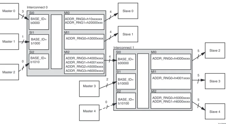
Figure 10shows an example of cascading two AXI Interconnect instances.
Figure 10 shows the following:
• MI slot #2 of AXI Interconnect 0 connects to SI slot 0 of AXI Interconnect 1. The endpoint slave devices #2-4 have address ranges as defined for MI slots #0-2 of AXI Interconnect 1.
Note: For conciseness, BASEADDR-HIGHADDR pairs are represented as ADDR ranges with don’t cares.
• The complete set of all address ranges accessible by Interconnect 1 are listed as multiple address ranges for MI slot #2 of Interconnect 0.
• The arrows represent the ID signals propagated from each master device. AXI Interconnect 0 produces 4 bits of ID output, which is the smallest width possible to keep the master IDs unique. For example, when Master 0 issues a transaction, the output ID is its master ID (1’b0) followed by 3 bits of ID sampled from the master device.
• All transactions from Master 2 have ID value 4’b1010 (no variable thread bits from the master device). • When a transaction from Master 0-2 targets Slaves 2-4, the AXI Interconnect 0 passes a 4-bit ID value to
Interconnect 1. Interconnect 1 then prefixes it with 1'b0 (the Master ID of its SI slot #0) to produce a 5-bit ID that it passes to any of the connected slave devices.
Multiple Address Range Support
The AXI Interconnect core must determine which MI slot is the target of each transaction by decoding the address of each AW and AR channel transaction from the SI slots. This address decode involves only those upper-order address bits needed to distinguish between MI slots and ignores lower-order bits that might be used to distinguish locations within the connected slave device. The entire address value received from the SI is presented to the MI and made available to the slave device. It is visible to any connected monitors, even though the high-order address bits are typically not reused by the slave device.
X-Ref Target - Figure 10
Figure 10: Cascading AXI Interconnect Cores
Master 0 Master 1 Master 2 Master 3 Slave 0 Slave 1 Master 4 Slave 2 Slave 3 Slave 4 5 5 5 ADDR_RNG0=h4000xxxx ADDR_RNG0=h10xxxxxx ADDR_RNG1=h20000xxx ADDR_RNG0=h3000xxxx ADDR_RNG0=h4000xxxx ADDR_RNG1=h4001xxxx ADDR_RNG2=h5000xxxx ADDR_RNG3=h6000xxxx ADDR_RNG0=h4001xxxx ADDR_RNG0=h5000xxxx ADDR_RNG1=h6000xxxx MI0 MI1 MI2 MI0 MI1 MI2 Interconnect 1 SI0 SI1 SI2 SI0 SI1 SI2 BASE_ID= b00000 BASE_ID= b10000 BASE_ID= b1000 BASE_ID= b10100 BASE_ID= b1010 BASE_ID= b0000 Interconnect 0 4 4 4 2 0 1 3 0 X12068
In some cases, there might be multiple, possibly disjoint, address ranges that define when a single slave device (MI slot) is accessed. The address decode logic in the AXI Interconnect core includes the multiple ranges that determine selection of each MI slot. Differentiation between the multiple address ranges is also typically required by the functionality of the connected slave device.
That typically means some of the decode logic implemented by the AXI Interconnect core is replicated in the slave device. The AMBA 4 specification introduces AXI signals AWREGION and ARREGION that can be used to encode the results of which address range is being decoded by the AXI Interconnect core. The AXI Interconnect core generates these REGION outputs for use by slave devices with multiple address decode ranges so that the range decode logic does not need to be replicated in the slave device.
The 4-bit value produced on each REGION signal corresponds to the position within the C_M_AXI_BASE_ADDR and C_M_AXI_HIGH_ADDR parameters, within each MI slot, that matches the transaction address. These address ranges are often represented using multiple parameters on the connected slave device, of a form similar to C_busif_RNGnn_BASEADDR and C_busif_RNGnn_HIGHADDR. See Figure 10 for an example of how multiple address ranges can be assigned to various MI slots.
Whenever a transaction address received on the SI does not match any of the ranges being decoded by the AXI Interconnect core, the transaction is trapped and handled by a decode error module within the AXI Interconnect core. An exception occurs when the AXI Interconnect core has only one MI slot and only one address range. In that case, the C_RANGE_CHECK parameter determines whether address decoding and associated decode error traps are implemented or whether all transactions are propagated to the MI slot.
Cyclic Dependency Avoidance
Any time there is more than one transaction ID (issued by one or more master devices) on which multiple outstanding transactions can be issued, and there is more than one connected slave device that can queue multiple transactions, and any of the slave devices can respond out-of-order on either the R or B channel, there is a potential cyclic dependency (deadlock) risk. Because the AXI Interconnect core is fully AXI-compliant, the AXI Interconnect core is equipped to handle slave devices that support out-of-order response.
How Deadlock Occurs
The following example shows how a sequence of Read transactions can result in deadlock. A similar situation also applies to a sequence of Write transactions when a slave device can reorder its Write response. This example shows a case where there are two master devices (M0 and M1) and two slave devices (S0 and S1) connected using the AXI Interconnect core:
1. Master device M0 reads from Slave device S0.
2. Master device M0 then reads from Slave device S1 (using the same ID thread). 3. Master device M1 then reads from Slave device S1.
4. Master device M1 then reads from Slave device S0 (using the same ID thread).
5. Slave device S0 responds to Master device M1 first. It re-orders the Read response, which is allowable because the received transaction IDs are different. However, the AXI Interconnect core cannot pass the response to Master device M1 because Master device M1 must first receive its response from Slave device S1.
6. Slave device S1 responds to Master device M0 (it does not re-order). But the AXI Interconnect core cannot pass the response to Master device M0 because Master device M0 must first receive its response from Slave device S0.
Avoiding Deadlock Using Single Slave Per ID
The method used in the AXI Interconnect core to avoid deadlock is “Single Slave per ID.” This method does not impact the performance of the transactions of most critical concern. These are the pipelining of multiple Reads and Writes, and by multiple master devices to a performance-critical slave device, such as a memory controller. The “Single Slave per ID” method imposes the restriction that each ID thread received at each SI slot (from each master device) can have outstanding transactions (of each type) to only one MI slot at a time.
However, MI slots are still permitted to issue multiple outstanding transactions from multiple SI slots.
By imposing this rule in the example shown in the previous section, the Read transaction from M0 to S1 in step 2 is stalled until S0 completes its response to M0. Similarly, the transaction from M1 to S0 in step 4 is stalled until S1 completes its response to M1. Whatever ways the transactions proceed forward under these conditions would avoid the interdependencies that could cause deadlock.
The” Single Slave per ID” restriction applies to all transaction threads whenever the AXI Interconnect core is configured as anything more complex than a 1-to-1 pass-through. Besides preventing deadlock, this restriction also guarantees in-order completion of all Write transactions at the SIs, even if different MI slots are targeted by a transaction thread in successive transactions.
For example, a master device writes to a DMA descriptor in memory, then writes to a control register in a DMA engine that subsequently reads that descriptor. Because the AXI Interconnect core does not allow the second Write to propagate to the DMA slave device until the first Write completes (Write response received from the memory controller), there is no risk that the DMA reads stale descriptor data from memory. Each master device is therefore guaranteed in-order completion of transactions to various slave devices, in the same direction, and on the same thread. Therefore, under those conditions, master devices do not need to condition subsequent Write transactions on receiving Write responses for prior transactions.
Note: AXI protocol provides no means to ensure in-order completion between Write and Read transactions other than waiting
for the B-Channel responses of all earlier writes to complete.
Error Signaling
The error conditions detected in the AXI Interconnect core are:
• Address decode error: No eligible MI slot mapped to the address of the transaction, according to the connectivity map and applicable Write-only/Read-only parameters. The AXI Interconnect core returns a DECERR and the transaction is not propagated to any MI slot. However, address decode errors are not trapped when the C_RANGE_CHECK parameter is set to 0. By default, C_RANGE_CHECK is enabled whenever there are multiple MI slots or if there are multiple address ranges. If the C_RANGE_CHECK parameter is forced to OFF (0) when there are multiple MI slots, any access to an illegal address might result in unpredictable and
non-compliant transaction propagation.
• AXI4-Lite access violation: Either of the following conditions:
• Burst length violation: Transaction length >1 data beat when targeting an AXI4-Lite MI slot.
• Data size violation: Transaction data transfer size wider than 4 bytes when targeting an AXI4-Lite MI slot. The AXI Interconnect core returns a DECERR, and the transaction is not propagated to the MI slot. AXI4-Lite access violations are disabled when C_RANGE_CHECK = 0. By default, C_RANGE_CHECK is enabled when any MI slots are configured as AXI4-Lite and any SI slots are configured as any protocol other than AXI4-Lite. If C_RANGE_CHECK is OFF (0), and an invalid transaction targets an AXI4-Lite MI slot, the results are unpredictable and the transaction will probably fail.
• An MI slot with C_M_AXI_SECURE set is targeted by a transaction in which AWPROT[1] or ARPROT[1] is set (unsecure).
Note: It is illegal to disable C_RANGE_CHECK if any MI slots are configured as SECURE.
The AXI Interconnect core does not detect the following error conditions:
• If the response ID received on an MI slot does not map to any SI slot, no READY response is issued from the AXI Interconnect core on the MI slot. The entire response (Write response or Read data burst) is permanently blocked by the AXI Interconnect core. This can cause the problematic slave device and any master device expecting to receive the response to hang.
• The AXI Interconnect core does not trap AXI4 protocol violations, which are the responsibility of the endpoint IP.
• The AXI Interconnect core neither supports nor traps Write data interleaving (all Write data is routed according to write transaction order; WID is not sampled at the SI).
• The AXI Interconnect core does not trap narrow burst violations. This occurs when an SI slot is configured with C_S_AXI_SUPPORTS_NARROW_BURST = 0 and it receives a transaction where there is a length > 1 data beat and the data transfer size is less than the SI slot data width, or any transaction in which AWCACHE[1] or ARCACHE[1] is deasserted. This is the responsibility of the endpoint master IP.
• Xilinx Platform Studio (XPS) enforces design rules that prevent erroneous configurations at compile time. Therefore, no error detection is provided by the AXI Interconnect core for these configuration errors: • Non-integer clock ratios when not configured for asynchronous clocking
• Parameter value range violations
AXI Protocol Converters
These subsections describe AXI protocol converters:
• AXI4-Lite Slave Conversion
• AXI3 Slave Converter
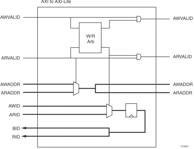
AXI4-Lite Slave Conversion
Each MI slot connected to an AXI4-Lite slave device routes through an AXI4-Lite conversion block. The conversion block single-threads all transactions, including single-threaded Round-Robin arbitration between Write and Read transactions. In most cases, Write and Read addresses are multiplexed onto a single bus, which is then duplicated onto the AWADDR and ARADDR signals of the MI slot. In most cases, because these duplicated signals are trimmed during back-end design implementation, the resources used by AXI4-Lite slaves are approximately the same as if there were only one address bus.
The transaction ID (AWID or ARID) is stripped and stored in the conversion block, and retrieved during response transfers as BID or RID.
Note: The AXI4-Lite protocol conversion does not convert AXI4/AXI3 bursts into a sequence of single-beat transactions for
AXI4-Lite slaves to minimize the resource utilization of the AXI4-Lite solution. Master devices accessing AXI4-Lite slave devices are expected to issue only single-beat transactions in which the SIZE of the data transfer is not greater than 32 bits.
Figure 11 illustrates the AXI4-Lite conversion logic.
X-Ref Target - Figure 11
Figure 11: AXI4-Lite Conversion Logic AXI to AXI-Lite AWVALID ARVALID AWVALID ARVALID AWADDR ARADDR AWADDR ARADDR AWID ARID BID RID W/R Arb X12067
AXI3 Slave Converter
A set of AXI3 slave conversion modules is instantiated at each MI slot connected to an AXI3 slave device, if the MI slot is accessible by one or more AXI4 SI slots.
This module receives an AW or AR transfer (command) on its slave interface and produces one or more commands on its MI, similar to the address channel downsizer module. The data transfer SIZE is never modified by the AXI3 converter. Any time a burst longer than 16 data beats is received, the command is split into a number of shorter burst transactions.
The AXI3 converter module normally allows multiple outstanding transactions to be propagated. Transaction characteristics from the AW/AR channel transfers are queued while awaiting corresponding response transfers. However, due to the possibility of write response and read data re-ordering, transaction acceptance by the AW and AR channel converter is restricted to a single outstanding transaction at a time (for each direction) whenever the transaction requires splitting.
I/O Signals
This section lists the AXI Interconnect core signals.
In Table 3, Table 4, page 29, Table 5, page 31, Table 6, page 32, Table 7, page 33, and Table 8, page 37, the “Default”
column shows whether the input signal is required (REQ) or, if not, its default value if left unconnected. Signal connections are required only for the SI and MI slots that are used. Values in the Default column also provide the protocol mode of the slot: AXI4 and AXI3, or “Lite” for AXI4-Lite. Input signals that are not sampled (do not care) for AXI4-Lite are indicated by “d/c”.
Slave Interface I/O Signals
Table 3 lists the Slave Interface signals. In the Width column “N” refers to the total number of SI slots, which is the
number of master devices connected to the AXI Interconnect core.
When deployed using the CORE Generator tool flow, each of the signal names listed in Table 3 takes the form “Snn_AXI_signalname”, where nn is the 2-digit index number (with leading zero) of each Slave Interface. In the Width column, N = 1 for all signals on the CORE Generator core interface.
Table 3: Slave I/O Signals
Signal Name Direction Default Width Description (Range)
S_AXI_ARESET_OUT_N Output N*1
Reset output (active-Low)
resynchronized to each slot’s clock. (This is not a signal defined by AXI protocol)
S_AXI_ACLK Input REQ N*1 Clock
S_AXI_AWID Input AXI3, AXI4: 0
Lite: d/c N*C_AXI_ID_WIDTH Write Address Channel Transaction ID
S_AXI_AWADDR Input REQ N*C_AXI_ADDR_WIDTH Write Address Channel Address
S_AXI_AWLEN Input AXI3, AXI4: 0
Lite: d/c N*8
Write Address Channel Burst Length (0-255)
S_AXI_AWSIZE Input
AXI3, AXI4:
REQ(1)
Lite: d/c
N*3 Write Address Channel Transfer Sizecode (0-7)
S_AXI_AWBURST Input
AXI3, AXI4:
REQ(1)
Lite: d/c
S_AXI_AWLOCK Input AXI3, AXI4: 0
Lite: d/c N*2
Write Address Channel Atomic Access Type (0, 1)
S_AXI_AWCACHE Input AXI3, AXI4: 0
(2)
Lite: d/c N*4
Write Address Channel Cache Characteristics
S_AXI_AWPROT Input 0b000(3) N*3 Write Address Channel Protection Bits
S_AXI_AWQOS(4) Input AXI4: 0
Lite: d/c N*4
AXI4 Write Address Channel Quality of Service
S_AXI_AWUSER(5) Input AXI3, AXI4: 0
Lite: d/c N*C_AXI_AWUSER_WIDTH User-defined AW Channel signals
S_AXI_AWVALID Input REQ N*1 Write Address Channel Valid
S_AXI_AWREADY Output N*1 Write Address Channel Ready
S_AXI_WID(5) Input 0 N*C_AXI_ID_WIDTH
Write Data Channel Transaction ID for AXI3 masters (sampled and propagated only when the interconnect is in pass-through mode between AXI3 endpoints).
S_AXI_WDATA Input REQ N*C_S_AXI_DATA_WIDTH Write Data Channel Data
S_AXI_WSTRB Input all ones N*C_S_AXI_DATA_WIDTH/8 Write Data Channel Byte Strobes
S_AXI_WLAST Input AXI3, AXI4: 0
Lite: d/c N*1 Write Data Channel Last Data Beat
S_AXI_WUSER(5) Input AXI3, AXI4: 0
Lite: d/c N*C_AXI_WUSER_WIDTH User-defined W Channel signals
S_AXI_WVALID Input REQ N*1 Write Data Channel Valid.
S_AXI_WREADY Output N*1 Write Data Channel Ready.
S_AXI_BID Output N*C_AXI_ID_WIDTH Write Response Channel Transaction ID.
S_AXI_BRESP Output N*2 Write Response Channel Response Code (0-3).
S_AXI_BUSER(5) Output N*C_AXI_BUSER_WIDTH User-defined B Channel signals.
S_AXI_BVALID Output N*1 Write Response Channel Valid.
S_AXI_BREADY Input REQ N*1 Write Response Channel Ready.
S_AXI_ARID Input AXI3, AXI4: 0
Lite: d/c N*C_AXI_ID_WIDTH Read Address Channel Transaction ID.
S_AXI_ARADDR Input REQ N*C_AXI_ADDR_WIDTH Read Address Channel Address.
S_AXI_ARLEN Input AXI3, AXI4: 0
Lite: d/c N*8
Read Address Channel Burst Length code (0-255).
S_AXI_ARSIZE Input
AXI3, AXI4:
REQ(1)
Lite: d/c
N*3 Read Address Channel Transfer Size code (0-7).
S_AXI_ARBURST Input
AXI3, AXI4:
REQ(1)
Lite: d/c
N*2 Read Address Channel Burst Type (0-2).
S_AXI_ARLOCK Input AXI3, AXI4: 0
Lite: d/c N*2
Read Address Channel Atomic Access Type (0, 1).
S_AXI_ARCACHE Input AXI3, AXI4: 0
(2)
Lite: d/c N*4
Read Address Channel Cache Characteristics.
Table 3: Slave I/O Signals (Cont’d)