Copyright by
Cheng-Chih Hsieh 2017
The Dissertation Committee for Cheng-Chih Hsieh
certifies that this is the approved version of the following dissertation:
Cerium Oxide Based Resistive Random Access Memory
Devices
Committee:
Sanjay K. Banerjee, Supervisor Davood Shahrjerdi, Co-Supervisor Jack Lee
Edward Yu Gary Gibson
Cerium Oxide Based Resistive Random Access Memory
Devices
by
Cheng-Chih Hsieh,
DISSERTATION
Presented to the Faculty of the Graduate School of The University of Texas at Austin
in Partial Fulfillment of the Requirements
for the Degree of
DOCTOR OF PHILOSOPHY
THE UNIVERSITY OF TEXAS AT AUSTIN December 2017
Acknowledgments
I wish to thank the multitudes of people who helped me through these years. First and foremost, I would like to begin by thanking my advisor at University of Texas at Austin, Dr. Sanjay K. Banerjee, for his support during my graduate studies at U.T. Austin. His intelligence and kindness, along with his academic council and membership truly enabled the completion of my degree. I am very grateful for his guidance and support. Secondly, I would like to thank my co-advisor at New York University, Dr. Davood Shahrjerdi, for his insightful advice and passion in research. He continually and convincingly conveyed a spirit of adventure in regard to research and scholarship. Without his guidance and persistent help this dissertation would not have been possible. I would also like to thank Dr. Jack Lee, Dr. Edward Yu, and Dr. Gary Gibson for taking the time to serve on my dissertation committee.
I would like to thank administrative and technical staffs of the Mi-croelectronics Research Center for their unfailing and continuous support. I sincerely thank Jean Toll for her assistance and support when dealing with University purchases, tuition issues, academic deadlines. The front office staff, led by Dr. James Hitzfelder, always provides professional and instant help when I have problems with logistics and safety concerns.
and cleanroom staffs of the Microelectronics Research Center. Garcia Ricardo, Jesse James, Bill Ostler, Johnny Johnson, and Marylene Pallard. It’s impossi-ble to keep cleanroom tools functional without their support and maintenance. They also trained me on several tools which are important for my research and kindly shared with me about tips for operating on those tools. Their relentless dedication are pillars for supporting the Microelectronics Research Center.
Next I would like to express my sincere gratitude to graduate students in the Microelectronics Research Center for their camaraderie. William Hsu, my best friend in my life, and also my colleague in the group. The days we studied together and chats in the cleanroom are unforgettable. Tanuj Travedi trained me essential skills for being a good teaching assistant of Integrated Circuits Nanomanufacturing Techniques. The memories we worked together for the course will last forever in my mind. My studies on cerium oxide would not have been possible without highest quality film grown by Dr. Anupam Roy. He is also a great mentor for life. Hema Chandra Prakesh and Amritesh Rai provided a lot of help for performing electrical characterization and logistics of lab inventory. Stephen Szczepaniak offered helps for correct my awkward grammar for the thesis. Rik Dey and Tanmoy Pramanik helped me grow cerium oxide thin films.
Last but not the least, tremendous gratitude goes to my family for all their endless love and encouragement. I am forever indebted to my parents for giving me the opportunities and experiences that have made me who I am. Smiles of my beloved daughter, Emma, always propel me forward to
accom-plish my dreams. At the end I would like express the deepest appreciation to my dear wife, Yoshie Mitsui, who spent sleepless nights with and was always my support in the moments when I need her. This journey would not have been possible if not for them, and I dedicate this milestone to them.
Cerium Oxide Based Resistive Random Access Memory
Devices
Publication No.
Cheng-Chih Hsieh, Ph.D.
The University of Texas at Austin, 2017
Supervisors: Sanjay K. Banerjee Davood Shahrjerdi
Resistive Random Access Memory (RRAM) is an emerging technology of non-volatile memory (NVM). Although the observation of metal oxide that can undergo an abrupt insulator-metal transition into a conductive state has been known for over 40 years, researchers started investigating those materials for memory applications in late 1990s. It has been considered as the next gen-eration memory technology to replace current flash memory because RRAM has demonstrated feasible switching characteristics and potential to build high density arrays and also RRAM is also compatible with contemporary CMOS processes, which means RRAM can be integrated into current CMOS chips. While the structure of RRAM is a simple metal-insulator-metal (MIM) device, there are numerous materials that exhibit resistive switching. The switching behavior is not only dependent on the switching layer materials but also depen-dent on the choice of metal electrodes and their interfacial properties. Many
metal oxides such as hafnium oxide (HfO2), titanium oxide (TiO2), aluminum oxide (Al2O3), nickel oxide (NiO), tantalum oxide (TaO2) and etc. have been studied in details; however, some materials are unexplored such as cerium ox-ide. In addition to nonvolatile storage applications, RRAM is considered as one of essential elements for advancing neuromorphic computing because of its analog switching and retention characteristics. This thesis investigated CeOx
-based RRAMs, from its fundamental device characteristics to neuromorphic applications.
Table of Contents
Acknowledgments v
Abstract viii
List of Figures xii
Chapter 1. Introduction 1
1.1 Memory Technology . . . 1
1.2 Resistive Random Access Memory . . . 4
1.3 Current state of Research . . . 6
1.4 Chapter Overview . . . 9
Chapter 2. Characterization of Cerium Oxide RRAM 13 2.1 Introduction . . . 13
2.2 Fabrication . . . 14
2.3 Electrical and Physical Characterization . . . 15
2.4 Conclusion . . . 23
Chapter 3. Bilayer Cerium Oxide RRAM 27 3.1 Introduction . . . 27
3.2 Hafnium Oxide and Cerium Oxide Stacked Resistive Random Access Memory . . . 30
3.3 Conclusion . . . 42
Chapter 4. Selector Device for RRAM 45 4.1 Introduction . . . 45
4.2 S-type NDR Niobium Oxide . . . 46
4.3 Back-to-back Schottky Diode . . . 54
Chapter 5. Short Term Relaxation of RRAM 65
5.1 Introduction . . . 65
5.2 Device Fabrication and Measurement . . . 66
5.3 Results and Discussion . . . 67
5.4 Conclusion . . . 74
Chapter 6. Neuromorphic Applications 75 6.1 Introduction . . . 75
6.2 Supervised and Unsupervised Learning . . . 76
6.3 Neural Networks . . . 79
6.4 Device Fabrication . . . 80
6.5 Single Hidden Layer ANN for Simple Image Recognition . . . . 81
6.6 Multiclass Image Recognition . . . 86
6.7 Simple Convolutional Neural Network for Image Recognition . 88 6.8 Conclusion . . . 96
Chapter 7. Conclusions 97 7.1 Summary . . . 97
7.2 Recommendations for Future Work . . . 99
Index 101
Bibliography 102
List of Figures
1.1 The current memory technology spectrum and emerging mem-ory technologies. Note that register, cache and DRAM are con-sidered as volatile memory, whereas SSD and HDD are consid-ered as NVM. . . 2 1.2 (a) Schematic of MIM structure for metaloxide RRAM. (b) (c)
Schematic of IV characteristics, showing two modes of opera-tion: (b) unipolar and (c) bipolar . . . 6
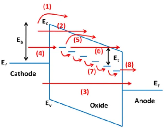
1.3 Schematic of the possible electron conduction paths through a MIM stack. (1) Schottky emission: thermally activated elec-trons injected over the barrier into the conduction band. (2) FowlerNordheim (FN) tunneling: electrons tunnel from the cath-ode into the conduction band; usually occurs at high field. (3) Direct tunneling: electron tunnel from cathode to anode di-rectly; usually occur when the oxide is thin enough. If the oxide has substantial number of traps (e.g., oxygen vacancies), trap-assisted tunneling contributes to additional conduction, in-cluding the following steps: (4) tunneling from cathode to traps; (5) emission from trap to conduction band, which is essentially the PooleFrenkel emission; (6) FN-like tunneling from trap to conduction band; (7) trap to trap hopping or tunneling, maybe in the form of Mott hopping when the electrons are in the local-ized states or maybe in the form of metallic conduction when the electrons are in the extended states depending on the over-lap of the electron wave function; and (8) tunneling from traps to anode. Adapted from [1]. . . 11 1.4 (a) shows the analogy of biological a neuron/synapse connection
and electrical representation of neuron/synapse. (b) shows a typical RRAM array representing an artificial neural network.[2] 12
2.1 Upper right panel shows that the etchant before etching reac-tion is white while lower right panel shows the etchant becomes Persian blue after etching. Left panels show color change of bulk CeOx film after etching. . . 16
2.2 (a) The typical dc sweep I-V characteristics of Al/CeOx/Au
structure. Arrows and numbers indicate the sweeping direction and order. The size of each device is 100µm dot in diameter and sandwiched structure of 30 nm Au, 13nm CeOx, and 30nm Au.
(b) Cross-sectional TEM image with Fast Fourier Transform (FFT) graphs in inset show thickness of each layer. Lattice constant is 5.4˚A at pristine state and 3.93˚A at LRS. . . 18
2.3 (a) Ce 3d core-level XPS spectra of MBE and PVD samples. The three-lobed envelopes structure of Ce 3d XPS spectra is due to multiple final states from Ce4+ and Ce3+. Arrows and symbols are referred to different final states and oxidation state of Ce. Note that symbols with blue color such as u000 , u00, u, v000 , v00, and v are final states from Ce4+; symbols with green color such as uo and vo are finals states from Ce3+. Other two final
states like lo and to are not shown in this figure due to relatively low amplitude and little contribution to the three-lobed envelop structure. (b) O 1s XPS spectra of MBE and PVD samples. The binding energy value of peak of MBE sample is higher than PVD sample, which means MBE sample has more Ce3+ component than PVD sample. . . 21
2.4 (a) HRS and LRS resistance along with switch cycles. The structure of tested device is 30 nm Al/13 nm PVD grown CeOx/30
nm Au at room temperature. (b) HRS and LRS resistance un-der a continuous 300-mV read voltage. The structure of tested device is 30 nm Al/13nm PVD grown CeOx/ 30 nm Au at room
temperature and 150◦C. The voltage sweep followed the numer-ical order in Fig. 2.2(a) for each cycle. Step 1: voltage ramps up to 2.5 V. Step 2: voltage ramps down to 0V, after this half cycle, voltage ramps up to 300mV to read and records the re-sistance. Step 3: voltage ramps up to -2.2 V. Step 4: voltage ramps down to 0V. Then, voltage ramps up to read and records the resistance. . . 24 2.5 (a) and (b) Diameter of device versus set voltage and reset
volt-age of MBE grown CeOx RRAMs. (c) and (d) Diameter versus
set voltage and reset voltage of PVD grown CeOx RRAMs. For
each area value, 20 devices have been tested. Inset graphs in (a) and (b) represent the LRS and HRS resistance dependence of MBE devices and inset graphs in (c) and (d) represent the LRS and HRS resistance dependence of PVD devices. . . 25
2.6 (a) and (b) Switching layer thickness dependence of forming voltage with MBE and PVD grown thin film. (c) and (d) Set voltage is independent of CeOx film thickness for both MBE
and PVD CeOx film. For each thickness value, 15 PVD and
MBE grown CeOx RRAM devices have been tested. . . 26
3.1 Improving memristor device characteristics using an engineered sub-stoichiometric HfOx capping layer. (a) Schematic structure
of two memristors with and without the engineered HfOx,
con-ceptually illustrating the increase of the oxygen vacancy density in the CeOx switching layer. This attribute of the bilayer
mem-ristor results in the forming-free operation and the reduction of the Set voltage. XPS spectra of the (b) engineered HfOx, and
(c) CeOx films with and without the HfOx capping layer. The
XPS studies indicate the increase of the oxygen vacancy concen-tration in the CeOxfilm capped with the oxygen-deficient HfOx
layer. (d) Representative current-voltage characteristics of two memristors, indicating the sub-1V operation of the bilayer mem-ristive device. (e) Heat transfer simulations illustrate enhanced Joule heating in the bilayer structure, causing the marked re-duction of the Reset voltage (scale bars are 2nm). The observed increase in Joule heating arises from the high thermal resistivity of HfOx at nanoscale. The thickness of HfOx is 2nm and the
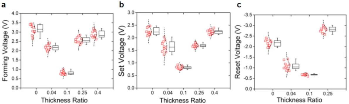
3.2 Effect of HfOx thickness ratio on the memristor device
behav-ior. The data indicates that the optimal device characteristics ((a) forming voltage, (b) Set voltage, and (c) Reset voltage) oc-curs at the thickness ratio of about 0.1. Moreover, the device-to-device variation is reduced at this optimal thickness ratio. The equivalency of the forming and Set voltages at the opti-mal thickness ratio confirms the forming-free operation of the device. Low device variability is critical for implementation of large neural networks with high density of memristive synaptic connections. Therefore, we statistically examined the effect of the HfOx thickness on the important device parameters: Set,
Reset, and forming voltages. In these experiments, the HfOx
thickness was varied, while keeping the total thickness of the bilayer stack fixed at 20nm. The thickness ratio defined in this work is HfOx thickness to total thickness in bilayer. The data
in Figure 3.2 indicates that the insertion of an HfOx capping
layer with the optimal thickness ratio of about 0.1 significantly improves the uniformity of the key device parameters. Interest-ingly, this optimal thickness ratio also coincides with the min-imum operating voltages of the bilayer structure. We surmise that the HfOx film begins to act as an independent switching
layer beyond this optimal thickness ratio, resulting in significant increase in both the device operating voltages and the device variability. Moreover, the Reset voltage begins to increase as the HfOx film becomes thicker. This observation is in
agree-ment with our heat transfer simulation results in Figure 3.3. In xviii
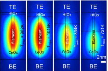
3.3 Effect of HfOx film thickness on Joule heating. Numerical heat
transfer simulation results for several bilayer HfOx/CeOx
struc-tures with varying HfOx to total thickness ratio at the bias
voltage of -0.6V. The total thickness of the HfOx/CeOx stack
was kept at 20nm. The Joule heating begins to diminish as the thickness of the HfOx was increased, which arises from the
thickness dependence of the HfOx thermal conductivity. . . 37
3.4 Device reliability studies. (a) The endurance test results for the CeOx and the optimal HfOx/CeOx devices. In addition to
the improved endurance properties, the bilayer device exhibits larger HRS and LRS values compared to the device with no HfOx. The increase of the LRS and HRS values is favorable
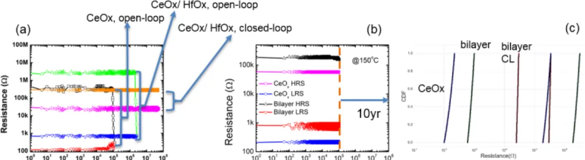
for reducing the switching power consumption of the bilayer device. Besides, when bilayer device were tested in close loop with adaptive programming and relaxed on-off ratio, it survives over 5×10⁷cycles without any degradation. (b) The accelerated retention test for the CeOx and the HfOx/CeOx devices
mea-sured at 150C at constant stress voltage of +0.2V. The results indicate projected data retention of 10 years for both devices. (c) Representative CDF plot of the cycle-to-cycle programing characteristics for two devices with and without the engineered HfOx layer. . . 39
3.5 Analog memory characteristic of the bilayer memristor. The normalized conductance of (a) bilayer memristor is plotted as a function of pulse widths and amplitudes when the device switches from a, fully Off state to fully On state, and (b), fully On state to fully Off state. The dashed lines are guide to the eye and the hatched regions denote unmeasured points. The data in (a), and (b) reveal the gradual change in the conduc-tance of the device between the fully Off and On states. Full On/Off switching energy consumptions of 2.6 and 2.1pJ were calculated from the transient (c), Set and (d), Reset voltage and current waveforms, respectively. . . 41 3.6 Switching cycles of intermediate states. Cycle test is conducted
in both positive polarity and negative polarity to examine if in-termediate states are separable and stable. The pulse voltage increased after every 100 cycles in (a) and (b). The resistance variation in each resistance state is very small1, which means it is very stable. The separation of each resistance state is not linear with applied voltage. But it has potential to generate more resistance states if more voltage interval are added be-tween each applied voltage properly. This also shows that the switching energy between each intermediate state is at femto joule scale . . . 42
3.7 Implementation of STDP learning using the HfOx/CeOx
mem-ristive device. (a) Schematic representation of the learning ex-periment. Two waveforms with identical shapes were applied to the top and bottom electrodes. In the learning experiments, the time intervals between the pre- and post-synaptic spikes were varied in order to probe the synaptic depression (δt<0) and po-tentiation (δt>0). The positive (negative) time difference indi-cates that the pre-synaptic spike occurs before (after) the post-synaptic one. (b) The plot clearly indicates the marked change in the synaptic strength as a function of different pre/post spike intervals. . . 43 3.8 Generation of waveforms for Spike-Timing-Dependent
Plastic-ity (STDP) measurements. Multiple square waves with vari-ous pulse heights were tailored for emulating exponential decay pulses used in STDP studies. The time interval of the pulses on the top and bottom electrodes (that are pre- and post-neural spikes) was varied relative to each other while monitoring the conductance of the device. The pulses were created using the Keysight B1500 pulse generator unit. Depending on the time difference between the pulses illustrated in Figure 3.8(a) and (b), the device demonstrates long-term depression (δt<0) and potentiation (δt >0) . . . 44
4.1 Bright field cross-sectional TEM image ofarepresentative NbOx
selector. Active area of NbOx is assumed to be at a uniform
temperature TN that is higher than the surrounding ambient
temperature, Tamb, due to Joule heating. This heated region is
thermally connected to Tamb through the effective thermal
re-sistance, Rth, and thermal capacitance, Cth, of the surrounding
device structures. . . 49 4.2 I-V curves of two different electroforming processes. Numbers
indicate order of sweeps; arrows indicate time evolution. (a) Type I forming. This results in increasing currents as the ini-tially amorphous Nb2O5 is reduced through interaction with the TiN electrodes. (b) Type II forming. This includes crystalliza-tion to a more resistive tetragonal NbO2 state after the initial reduction. The slope of curve 5 in (b) is positive at high currents due to a ∼100 Ω resistance in series with the selector. . . 51 4.3 (a) Measured (solid) and calculated (dashed) V-I curves for
TiN/NbOx/TiN selector with 52 nm diameter bottom electrode
and 8 nm thick NbOx layer for Tamb = 275−450 K. (b)
Arrhe-nius plot of the conductance measured at biases low enough for it to be ohmic. . . 54
4.4 (a) DC I-V characteristics from two-dimensional numerical sim-ulation by Sentaurus from Synopsys Inc.. Two orange dashed lines represent voltage values calculated for NL ratio. The choice of 1MA/cm2 is based on matching current density of RRAM devices. (b) I-V characteristics on Schottky barrier height dependence. Note that non-linear step size of simula-tion caused I-V curves to show a small hysteresis at low bias during positive polarity sweep, which is an artifact. (c) NL ratio extracted from Figure 4.4(a)(b). . . 58 4.5 (a) Band diagrams at equilibrium and forward bias on D1. The
equivalent circuit diagram was shown at forward bias on D1. Series resistance is labeled as RS.φb1 andφb2represents Schottky barrier height at D1 and D2. (b) Cartoon illustration of cross-sectional view of device. The green arrow indicates the effective area of device. . . 59
4.6 (a) Semilog plot of I-V characteristics of different thickness Ti−aSi−Ti diodes. The dashed circle is where series resistance effect becomes prominent. (b) I-V characteristics of Ti−aSi−Ti and Ni−aSi−Ni with 10 nm amorphous silicon. (c) Comparison of the NL ratio between Ti−aSi−Ti and Ni−aSi−Ni at different thickness. The inset of (c) is linear scale I-V characteristics of (b). (d) I-V curve fitting by using (7). (7) fits well at interme-diate bias where series resistance effect was low and thermionic emission is dominant. . . 63 4.7 (a) Pulse measurement setup and impedance at each stage.The
pulse generator has an output impedence of 50 Ω, and input channel impedance of oscilloscope is 50 Ω as well. (b) shows the transient current response of DUT. Black curve and arrow is input pulse generated by source and blue curve and arrow is current response of MSM diode. The device is a 300 nm ×300 nm crossbar. . . 64 4.8 (a) Test scheme of cycle test. (b) Endurance test up to 108
5.1 Green and black curves in Figure 5.1 are initial resistance of HRS and LRS after programming to RRAM cell. Blue triangles and red dots are resistance after given time delay. From left to right, the time delay between initial read and delay read is 100
µs, 1ms ,and 1s, respectively. . . 66 5.2 Schematic illustration of the adaptive programming algorithm.
Read pulses are 200ns at 0.2V. Write pulses start at 0.2V with 0.1V increment. The interval between each pulse is 10µs. At each attempt to switch the resistive state of the device, a write pulse is applied to the RRAM device followed by a read pulse to check whether the value of the read current is higher(lower) than the target value during the SET(RESET) cycles. If this condition is met, we consider this attempt as a successful SET (RESET). . . 68 5.3 Testing setup for fast sampling measurement. LabView software
was used for programming and controlling FPGA and Python was used for data processing after data collecting by FPGA and LabView. . . 69 5.4 Distribution of HRS and LRS read currents for (a) 1R and (b)
1S1R structures. . . 70 5.5 RTN noise at different current amplitude of MSM selector. (a)
5.6 CDF plots using probit units for (a) 1S1R, (b) 1R with 100ns forming pulse, and (c) 1R with 5µs forming pulse. The arrows labeled ”time” in (a) indicate the temporal progress of the ex-periment. The horizontal arrows indicate the gap between tail bits of the HRS and the LRS. Probit of the HRS curves are plot-ted in a decreasing fashion versus current, while the LRS curves are plotted in an increasing fashion versus current. The read pulse voltage in (a) is 1.7V because of voltage drop at selector device. . . 71 5.7 Effect of the operating window and the forming pulse duration
on the long-term reliability endurance of RRAMs. Devices were subject to the adaptive programming with a read pulse width of 200 ns. . . 73 6.1 The I-V characteristics of voltage contorlled generic
memris-tor can be derived from state dependent Ohm’s law and state equation. The I-V curve shown here is from a sinusoidal voltage source.[3] . . . 77 6.2 Yellow circle represents supervised learning and blue circle
rep-resents unsupervised learning. The intersection of two circles is the ”intermediate” learning. . . 78
6.3 The black crosses and smiley faces represent the input data for classification. The red dashed line is the SVM classifier. The gray triangles in the right diagram represent the input data for clustering. . . 79 6.4 Schematics representation of ANN. The activation function of
synapse in the hidden layer is a delta function. The total num-ber of input neurons is R. Total numnum-ber of synapse in the hidden layer is M. . . 81 6.5 Optical microscope images of a 10×10 RRAM array are at left
and 30 degree tilted and top view SEM images are at right. . 82 6.6 The input training data was encoded to input signals for
train-ing neural networks. Red pixels in traintrain-ing data were converted to hot for non-inverted neural network and blue pixels were converted to hot for inverted neural network. . . 83 6.7 Testing data was encoded into input signals for each column,
then passing to all columns in each neural network. The result is based on comparison of current between non-inverted array and inverted array. . . 84
6.8 (a) represent a RRAM device with nonlinear weight change function versus in a crossbar array. The dashed line in the middle represents the ideal linear weight change. (b) shows the device-to-device variation from 10 RRAM devices in the same array. (c) The prediction accuracy at different pulse voltage during the training. Note that there are two color groups in (c). The red one and blue one are results from different RRAM arrays. Note that the prediction accuracy is precision. Preci-sion in statistics is defined by the ratio of true positives over true positives plus false positives. . . 85 6.9 (a) represents different magnitude of non-linearity used in
Ten-sorFlow simulation for (c). (b) shows the result by TenTen-sorFlow simulation of device-to-device variation on prediction accuracy. Moderate nonlinear weight change is 2 in (a) and strong non-linear weight change is 4 in (a). (c) TensorFlow simulation of non-linearity on prediction accuracy. Note that the simulation assumes no device variation on RRAM synapses. . . 85 6.10 Training images used for multiclass image recognition. The left
images are ideal patterns for each class. . . 87 6.11 Training scheme for multiclass image recognition. The input
image encoded into signals and pass to the assigned columns in RRAM array. One column is trained with non-inverted signals, and the other is trained with inverted signals. . . 87
6.12 Testing scheme for multiclass image recognition. The non-inverted input passed to all columns. The prediction result is based on ”One-vs-All” method,i.e, each binary classifier provides its pre-diction and the final result is the one with maximum current. . 88 6.13 Prediction accuracy versus number of training data set. Note
that the prediction accuracy of each letter is based on definition of precision. And averaged accuracy is based on marco-average of precision. . . 89 6.14 A Simple CNN architecture with depth of three. The input
data is mapped to the feature layer with convolution by filter matrix. Then the feature layer is mapped to subsample layer by pooling. Finally, the classification is performed by a fully connected layer. The depth in CNN means the number of fea-ture layers used for convolution. Each feafea-ture layer might have different filter matrix. . . 90 6.15 The input data is convoluted with the filter matrix and mapped
to feature layer. Here, a 3×3 filter matrix is used for edge detection. The 3×3 pink matrix represents the feature layer. . 90
6.16 The synapses in the feature layer are divided into several pools, and pooling process chooses the maximum weight in each pool then mapping all to a subsample layer. The pool size is 2×2 and the size of feature layer is 4×4, therefore, the subsample layer is 2×2. Synapses in the subsample layer connects to a fully connected layer for classification. Synapses in fully connected layer sums up weights with blue arrows minus weights with red arrows. The fully connected layer provides classification result. 91 6.17 The filter matrix and connection between the subsample layer
and the fully connected layer is adapted from the result by Ten-sorFlow simulation. . . 93 6.18 Training scheme of the CNN. Note that during the training, the
write voltage is always 1.2V and no connection to the subsample layer. . . 94 6.19 Testing scheme of the CNN. The read voltage is 0.2V and the
output is based on the comparison of current from each sub-sample layer. . . 94 6.20 (a) Prediction accuracy of regular testing data set between
sin-gle hidden layer ANN and CNN. (b) Prediction accuracy of 50% ambiguous testing data set between single hidden layer ANN and CNN. . . 95
6.21 (a) Prediction accuracy of CNN with different filter matrix for ambiguous testing data set. The filter matrix is also shown in (a), the one at left is identity filter and the one at right is sharpen filter. (b) Prediction accuracy of each class for CNN with sharpen filter. . . 95
Chapter 1
Introduction
1.1
Memory Technology
In the ”Big Data” era, massive amount of data is stored in data centers and computed at the server end, which is also referred to as cloud computing. In future, the majority of data mining and machine learning problems will be solved in the ”cloud” instead of local machines because data set is too large to be handled efficiently on a local machine. The performance of cloud computing will strongly depend on the performance of the memory architecture and the memory technologies. Figure 1.1 shows the spectrum of the current memory technologies and emerging memory technologies: spin-transfer torque mag-netic random access memory (STT-MRAM), resistive random access memory (RRAM) and phase change random access memory (PCRAM). The left end of the spectrum represents fast, small capacity and volatile memory technologies, on the other hand, the right end of the spectrum represents slow, large capac-ity and non-volatile technologies. Current L1/L2/L3 cache, dynamic random access memory (DRAM), and solid state drive (SSD) are based on comple-mentary metal-oxide-semiconductor (CMOS) technology. These conventional memory technologies might not be able to meet the requirement with device scaling. Thus, these emerging memory technologies have been investigated
Figure 1.1: The current memory technology spectrum and emerging memory technologies. Note that register, cache and DRAM are considered as volatile memory, whereas SSD and HDD are considered as NVM.
wildly for volatile and non-volatile memory (NVM) applications.
STT-MRAM, PCRAM and RRAM are most popular candidates among all potential technologies and share some common properties such as: two-terminal device structure, non-volatile memory, device switches between a high resistance state (HRS) and a low resistance states (LRS). Two differ-ent resistance states can be used to store ”0” and ”1” for digital memory device. Nevertheless, the physics behind resistance state change is quite dif-ferent: STT-MRAM utilizes the parallel configuration and anti-parallel con-figuration of two ferromagnetic layers separated by a tunneling insulator layer to generate LRS and HRS. PCRAM uses chalcogenide compound for switch-ing between the crystalline phase and the amorphous phase to provide LRS and HRS. RRAM switches between LRS and HRS by modulating conductive filament length or interracial reaction on electrode to exchange oxygen
de-fects. These three technologies have different I-V characteristics because of their switching mechanisms. Table 1.1 compares the device performance of conventional CMOS based memory technologies and emerging memory tech-nologies. In Figure 1.1 the arrow of STT-MRAM has overlap with register and L1/L2/L3 cache, and the reason is well explained in Table 1.1. STT-MRAM has smaller area, lower switching energy, similar endurance and comparable read/write time compared to SRAM. Next, RRAM and PCRAM have sim-ilar overlap with SSD, HDD and DRAM in Figure 1.1, and it can be seen that both RRAM and PCRAM are better in terms of area, switching energy, read/write time and endurance. These make RRAM and PCRAM very at-tractive to replace NAND Flash for storage. Recently Intel Inc. and Micron Technology Inc. announced transistor-less NVM product, which is called 3D XPointTM. The product could use PCRAM or RRAM technology based on patents filed by both companies[4–6] and the array architecture revealed. In-tel Inc. claimed that the 3D XPoint NVM can be part of main memory like DRAM[7]. This indicates that RRAM and PCRAM have potentials to re-place DRAM. Although in Table 1.1 DRAM has faster read/write time and lower switching energy, RRAM and PCRAM do not require refresh to retain data; this can significantly improve the efficiency of the computing system. Furthermore, this will blur the borderline between volatile and non-volatile memory. These emerging NVM technologies can be revolutionary for memory subsystem design.
Table 1.1: Performance metrics of current and emerging memory technologies SRAM DRAM NAND Flash STT-MRAM PCRAM RRAM Area (F2) 140 6-12 1-4 20 4-16 <4
Switching energy (pJ) 0.0005 0.005 10-100 2-25 2-25 2.6 Read Time (ns) 0.1-0.3 10 25000 <2 10-50 <10 Write time (ns) 0.1-0.3 10 220000 <10 50-500 25 Retention N/A <1s yrs yrs yrs yrs Endurance >1016 >1016 104−6 >1015 109 108
1.2
Resistive Random Access Memory
As mention in the previous section, RRAM has been considered as one of the promising candidates for the next generation of NVM because of the fast write and read rates, long data retention time, and feasible scalability[8–10]. The resistive switching phenomenon was observed by Hickmott[11] in 1960s. The structure of RRAM is a simple metal-insulator-metal (MIM) device, and there are numerous materials that exhibit resistive switching. Figure 1.2 (a) provides the schematic of a common metal oxide RRAM cell.[1] The basic op-eration of RRAM is as follows: For the pristine samples in its initial resistance state, a larger voltage is needed to trigger the resistive switching behaviors for the subsequent cycles. This is called the electroforming or forming pro-cess. Forming is the process which forms certain phase or configuration so that the switching layer becomes conductive. After forming process RRAM is at high resistance state (HRS). The switching event from HRS to low resis-tance stae (LRS) is called the set process, which usually requires lower voltage. Conversely, the switching event from LRS to HRS is called the reset process. The switching modes of metal−oxide RRAM can be broadly classified into two switching modes: unipolar and bipolar, which depend on the choice of
materials stack for the RRAM cell. Unipolar switching means the switching polarity of set and reset processes is the same, and set or reset happens at cer-tain voltage amplitude. If the unipolar switching can symmetrically occur at both positive and negative polarity, then it is also called nonpolar switching. Bipolar switching means the switching polarity of set and reset depends on the polarity of the applied voltage. So set can only occur at one polarity and reset can only occur at the other polarity. For either switching modes, to avoid a permanent dielectric breakdown in the set process, the common practice is to apply current compliance if voltage sweep is selected (voltage compliance if current sweep is selected). This usually can be done by the semiconductor parameter analyzer, or transistor or rectifying diode. To read the data from the cell, similar to a flash memory, a small read voltage is applied to determine the memory state (HRS or LRS), without disturbing the memory state. Figure 1.2 (b)(c) demonstrates the concept of unipolar and bipolar switching. Note that even the same switching layer can demonstrate both unipolar and bipolar with different combinations of metal electrodes or different stoichiometric ratio of switching layer.
Many reports have studied the current transport mechanisms in LRS and HRS. Most reports show a linear or ohmic relationship in the LRS. How-ever, the conduction characteristics in HRS are quite different: Poole−Frenkel emission, [12, 13] Schottky emission [14, 15], the space charge limited current (SCLC) characteristic[16, 17] were observed in various metaloxide RRAMs. Figure 1.3 summarizes possible transport mechanisms in RRAM.
Figure 1.2: (a) Schematic of MIM structure for metaloxide RRAM. (b) (c) Schematic of IV characteristics, showing two modes of operation: (b) unipolar and (c) bipolar
1.3
Current state of Research
High dielectric constant binary transition metal oxide RRAMs have attracted a lot of interest because of operating voltage compared with sili-con dioxide RRAMs and Pr0.7Ca0.3MnO3 (PCMO). Besides, the fabrication is compatible with current CMOS process[18–20]. There are some materials also demonstrate decent resistive switching characteristics, for example, cerium ox-ide.
RRAM is a memory technology that can be integrated with conven-tional CMOS in a simple way, using a material set compatible with the con-ventional CMOS fabrication environment and process temperatures that al-low its integration at back-end-of-line (BEOL). Because of its al-low-temperature process, RRAM is often envisioned to be stacked in 3-D in a crossbar archi-tecture with an effective memory cell area of 4F2=n, where n is the number of 3-D-stacked memory layers[21]. At the system level, it is envisioned that
a revolution in memory hierarchy and system architecture will be realized by this low-cost, BEOL-compatible, nonvolatile memory with tens of nanosecond bit-alterable read/write speed, over 106 endurance cycles, and potentially low power/energy consumption.
To achieve implementing RRAM, many efforts have been made on memory cell design for optimal memory array design, 3D crossbar architec-ture. A current limiter, which can optimally constrain the forming/set current, is necessary for the filamentary switching device to prevent the degradation of HRS and even the failure of the memory device. A serial transistor with RRAM cell is a good candidate of current limiter than an external electrical measurement instrument because of faster response and very large resistance at saturation region. Special consideration must be taken for design of mem-ory cell of one-transistor-one-RRAM (1T1R) structure to avoid having a large parasitic capacitance between the transistor and the RRAM. The parasitic capacitance causes overshoot current during the forming/set process which in turn increases the reset current. Specifically, during the forming/set pro-cess, the RRAM resistance changes instantly while the voltage drop across the RRAM cannot drop instantly due to the presence of parasitic capacitance. Therefore, during the overshoot period that the voltage across the RRAM gradually decreases, excessive oxygen vacancies form and the conductive fila-ments (CFs) tend to grow laterally and increase in diameter or multiple CFs can be generated. Another popular candidate as current limiter is a bidirec-tional diode with non-linear I-V characteristics for a bipolar switching device
or a p-n diode for unipolar/nonpolar switching device. The advantage of this approach is that this has no area overhead compared to 1T1R scheme and it is easy to fabricate for 3D memory arrays. Such bidirectional diode should have high current density when it turns on and matching operating voltage with RRAM cell. It should not break down while forming process takes place (or RRAM cell is forming-free). There are still no conclusive results on such a bidirectional diode although many promising devices have been proposed, such as mixed ionic electronic conduction (MIEC)[22],VO2 utilizing metal-insulator transition[23], Ovonic threshold switch (OTS) [24] and Schottky diode[25].
What makes RRAM such an exciting technology is not only NVM applications, but also great potential for realizing neuromorphic computing paradigm. RRAM device behaves similarly to what memristor[26] should be like: RRAM retains its resistance state during switching. Some RRAM devices share similar properties with biological synapses, which is analog switching in conductance. This raises a lot of interest in RRAM for building neuromorphic computing system. Traditional Von-Neumann architecture has bottleneck in parallel computing due to the bandwidth limit between central processing unit (CPU) and memory. On the other hand, the brain-like architecture which em-ulates human brain functions overcome the bandwidth limit. Neuromorphic architecture provides several benefits in machine learning problems. One re-cent progress in machine learning is the development of deep learning. Deep learning utilizes the architecture of human brain neural networks, which com-prises pre-neurons, synapses and post-neurons. Pre-neurons and post-neurons
propagate or generate electrical signals to synapses and synapses are the key elements for learning. They received signals and update their weight accord-ingly. RRAM with analog switching is the ideal device to perform weight updating because of the similarity to biological synapse. Figure 1.4 shows a RRAM crossbar array for neuromorphic computing. Top and bottom electrode connect to CMOS neuron circuits; RRAM, which is called memristor in (a) is sandwiched by bottom electrode and top electrode, represents an electrical synapse.
1.4
Chapter Overview
This thesis investigates the fundamental electrical and physical char-acterization of cerium oxide based RRAM devices, bilayer RRAM devices, selector devices, short-term relaxation issue, and lastly, neuromorphic appli-cations. This chapter introduced background and current key issues related to NVM and RRAM technology. Chapter 2 studies the basic CeOx RRAM
device, starting from device fabrication, materials characterization to electri-cal characterization. Performance metrics are discussed in Chapter 2 as well. Chapter 3 addresses the issue of non-analog switching in reset operation for simple CeOx RRAM. The novel bilayer HfOx/CeOx is proposed in Chapter 3,
and the bilayer device provides several benefits compared to single layer CeOx
RRAM. Chapter 4 proposes metal-semiconductor-metal (MSM) diode as selec-tor device to eliminate leakage current in RRAM array. Chapter 5 discusses the origin of short-term relaxation issue in RRAM and combined RRAM/selector
structure. Chapter 5 demonstrates a potential solution to short-term relax-ation. Chapter 6 demonstrates the fabrication of RRAM arrays for nerual network based pattern classifiers. Various configurations of neural network are proposed and demonstrated. A conclusion is given in Chapter 7.
Figure 1.3: Schematic of the possible electron conduction paths through a MIM stack. (1) Schottky emission: thermally activated electrons injected over the barrier into the conduction band. (2) FowlerNordheim (FN) tunneling: electrons tunnel from the cathode into the conduction band; usually occurs at high field. (3) Direct tunneling: electron tunnel from cathode to anode di-rectly; usually occur when the oxide is thin enough. If the oxide has substantial number of traps (e.g., oxygen vacancies), trap-assisted tunneling contributes to additional conduction, including the following steps: (4) tunneling from cathode to traps; (5) emission from trap to conduction band, which is essen-tially the PooleFrenkel emission; (6) FN-like tunneling from trap to conduction band; (7) trap to trap hopping or tunneling, maybe in the form of Mott hop-ping when the electrons are in the localized states or maybe in the form of metallic conduction when the electrons are in the extended states depending on the overlap of the electron wave function; and (8) tunneling from traps to anode. Adapted from [1].
Figure 1.4: (a) shows the analogy of biological a neuron/synapse connection and electrical representation of neuron/synapse. (b) shows a typical RRAM array representing an artificial neural network.[2]
Chapter 2
Characterization of Cerium Oxide RRAM
2.1
Introduction
Similar to other high dielectric constant binary transition metal oxides, such as hafnium oxide and titanium oxide, cerium oxide has high dielectric constant and several valance states, making cerium oxide a potential material for RRAM application. Nevertheless, fundamental characterization of CeOx
based RRAMs, i.e., the scalability, reliability, and mechanism, has been only partially reported[27–29]. In this chapter, we demonstrate key characteristics of CeOx RRAMs. One of the prevailing explanations of resistive switching
is the formation of filament path in the switching layer. The typical RRAM device can be described as a sandwich MIM structure: an insulator thin film stacking on the first metal layer followed by second metal layer above the in-sulator film. The first metal layer is called bottom electrode (BE), and the second metal layer is called top electrode (TE). When the bias is applied on the insulator, oxygen vacancies build up filament paths, which change the re-sistance of MIM. This process is reversible. For bipolar RRAMs, applying the opposite polarity can reverse the process; the oxygen vacancies move back to bulk region of insulator. Certain types of MIM structure show unipolar switch-ing. Most binary transition metal oxide based RRAMs show bipolar switchswitch-ing.
Although some groups have already reported resistive switching of CeOxbased
RRAMs, there are still many unanswered questions and interesting behaviors of the system needed to be addressed, since cerium oxide is a relatively new material in the field. In this work, we report scalability, thickness dependence, endurance test, and mechanism discussion.
2.2
Fabrication
Devices were fabricated on a n-type Si (111) substrate with 300 nm plasma-enhanced chemical vapor deposition (PECVD) grown silicon dioxide on the top. Gold was used as the bottom electrode and deposited above the silicon dioxide layer by electron beam evaporation. Cerium oxide thin film was then deposited at room temperature (RT) by physical vapor deposition (PVD) in in situ oxygen plasma and molecular beam epitaxy (MBE) at 500 degree in Celsius. Then, devices were patterned by photolithography using AZ-5209 photoresist, followed by developing in AZ 726 MIF developer. The top electrode (500 nm - 300µm in diameter) was deposited by electron beam evaporation above the cerium oxide layer, and put in an acetone bath at room temperature for a day to lift off photoresist, followed by washing the device with acetone and isopropyl alcohol. The final step is to wet etch CeOx by
using the top electrode as hard mask; the etching solution is the mixture of hydrochloric acid, potassium hexacyanoferrate, K4[Fe(CN)6]·3H2O, and wa-ter. The mechanism of etching is based on cyanide ions forming coordination compounds with cerium ions. The detailed chemical reactions and solution
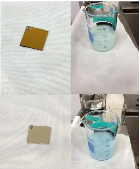
preparation were illustrated in the article by A.Kossoyet al..[30] Figure 2.1 shows color change of etchant and sample before and after reaction.
2.3
Electrical and Physical Characterization
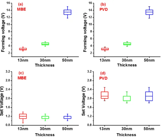
Electric characterization of devices were taken by Agilent Semiconduc-tor Parameter Analyzer B1500 and Lakeshore CRX-VF Probe Station. De-vices were measured by applying voltage to the top electrode while the bottom electrode is grounded. For most RRAMs, there are two basic operation modes called set and reset. When applying bias upon certain point, the current through RRAM suddenly rises; this process is called set. After set process, RRAM is at LRS. If RRAM is bipolar when the bias is applied with the op-posite polarity relative to the bias during the set process, the current will suddenly drop after a certain point. This process is called reset. After reset, RRAM is at HRS. The HRS appeared after reset process can be changed again to LRS by set. The resistance change between LRS and HRS is repeatable and nonvolatile. For the first voltage application on RRAM, usually it requires higher voltage to switch from HRS to LRS, this process is called forming and it is usually considered as a soft breakdown of the MIM structure. Dimension of each device is the same and MBE grown CeOxRRAM shows lower set and reset
voltage and larger operation window than PVD CeOxcounterpart. The
opera-tion window is defined as the ratio of resistance between HRS and LRS. These phenomena can be explained by difference in oxygen point defect mobility in CeOx film.[31] The decrease of the mobility of oxygen vacancy may result in
Figure 2.1: Upper right panel shows that the etchant before etching reaction is white while lower right panel shows the etchant becomes Persian blue after etching. Left panels show color change of bulk CeOx film after etching.
higher voltages needed to drive oxygen vacancies in the dielectric layer. MBE CeOx film has better interfacial properties at CeOx/Al interface, and thus less
pinning of oxygen vacancies. Superior operation window observed in MBE CeOx can be explained by difference in the effective defect levels. In the work
by Gouxet al.[32], CeOx film with high temperature process (750◦C) tends to
have higher activation energy (Ea = 320 meV), which means point defects are
more trapped. A similar mechanism may result in higher resistance values for the HRS in MBE film. Compared with other high- k dielectric based RRAM devices, such as TiO2, AlO3, and HfOx, both MBE and PVD CeOx based
RRAMs have competitive value of the operation window (104 for PVD CeO
x
and 106 for MBE CeO
x). MBE CeOx RRAM shows low set and reset voltage
(1.1 V for set, 0.9 V for reset, and 2.8 V for forming), making CeOx RRAM
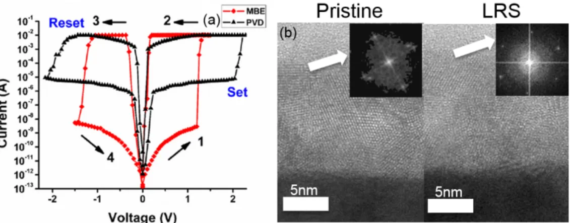
a suitable candidate for low power consumption applications. Figure 2.2(a) represents a typical dc-sweep of CeOx RRAM device.The physical dimension
of each device is the same and MBE grown CeOx RRAM shows lower set
and reset voltage and larger operation window than PVD CeOx counterpart.
Figure 2.2(b) shows cross-sectional transmission electron microscope (TEM) image of MBE grown CeOx RRAM at pristine state and LRS state. Insets
of Figure 2.2(b) show crystalline structure at each state. Lattice constant of crystalline structure near Al/CeOx interface calculated from analytic software
indicates that CeO2 is dominant phase at pristine state and more Ce2O3 at LRS. In addition, CeOx based RRAM devices can switch between HRS and
to 20 MHz.
Figure 2.2: (a) The typical dc sweep I-V characteristics of Al/CeOx/Au
struc-ture. Arrows and numbers indicate the sweeping direction and order. The size of each device is 100 µm dot in diameter and sandwiched structure of 30 nm Au, 13nm CeOx, and 30nm Au. (b) Cross-sectional TEM image with Fast
Fourier Transform (FFT) graphs in inset show thickness of each layer. Lattice constant is 5.4˚A at pristine state and 3.93˚A at LRS.
There are two prevailing hypothesis for the resistive switching mecha-nism in metal oxide based RRAMs. The first one is filamentary conduction in metal oxide. In this model, oxygen vacancies generated by applying a bias form filamentary conduction paths in dielectric. The formation and rupture of filament enable resistive switching in metal oxide based RRAM. The second one is called interface model. The change of oxidation state in memory ma-terials causes resistive switching. In NiO system by Kinoshita et al.[33], the resistance switching happened on the anodic side of the conductive filaments in NiO, which implied that the electrochemical reaction involved in resistive switching. The change in the oxidation state is analogous to anodic oxidation.
To understand the conduction mechanism and reason performance dis-crepancy between MBE CeOx and PVD CeOx, the chemical composition and
chemical bond condition of dielectric layer have been investigated by X-ray photoelectron spectroscopy (XPS). All XPS spectra were acquired at room temperature by Vacuum Generator Scientific SCALAB Mark II system and monochromatic Al KA (hν = 1486.7 eV) X-ray radiation source. The
back-ground pressure was kept below 7.5×10⁻⁸ Torr.[34] And the pass energy for high resolution spectra of Ce 3d and O 1s was 50 eV and 20 eV. Figure 2.3(a) shows Ce 3d XPS spectra of both MBE and PVD grown CeOx. The typical
Ce 3d XPS core-level spectra have three-lobed envelopes (around 882−890 eV, 895−910 eV, and 916 eV) due to different final states of a mixed valency.[35, 36] Note that u000 (v000), u00 (v00), and u (v) represent Ce4+ final states: Ce 3d94f0 O 2p6, Ce 3d94f1 O 2p5, and Ce 3d94f4 O 2p4, respectively, for Ce3d
3/2 and Ce3d5/2. Besides Ce4+ has three final states, Ce3+ final states also appear:
3d94f1 O 2p5 and 3d94f2 O 2p4, expressed as u0 (v0) and uo vo. Final states
configuration of Ce 3d XPS spectra have been studied previously[37, 38], and the focus on Ce 3d XPS spectra in this work is to distinguish and analyze the difference between MBE and PVD grown CeOx thus discuss the mechanism of
resistive switching in Al/CeOx/Au system. Arrows in Figure 2.3(a) indicate
different final states of Ce 3d XPS spectra and uo and vo have stronger
influ-ence on Ce 3d core-level XPS spectra than uo and vo do. The deconvoluted
components of Ce 3d XPS spectra structure have been discussed by Adnot and Bernis and Hasegawa et al.[35] In Figure 2.3(a), MBE Ce 3d XPS spectra
have higher amplitude of peaks than PVD Ce 3d spectra at 904 eV and 885 eV, which corresponds toµ0andν0components. In addition, O 1s spectra also show similar trend between MBE and PVD samples. Figure 2.3(b) shows O 1s spectra of both MBE and PVD grown CeOx thin film. O 1s peak of PVD
CeOx is less steep at lower binding energy side than O 1s peak of MBE CeOx
at lower binding energy side. The binding energy of O 1s in CeOx and Ce2O3
has been reported as 529.2 eV and 530.3eV, respectively. The difference of the binding energy implies that O 1s peak of MBE grown CeOx has more Ce2O3 than PVD grown CeOx. From XPS spectra results of Ce 3d and O 1s, it can
be concluded that MBE sample includes more Ce3+ than PVD sample. A report by Yoshitake et al. about cerium oxide based RRAM claims that the reduced cerium would inhibit the resistive switching in cerium oxide; however, in Al/CeOx/Au system, the influence of Ce3+ is not obvious. MBE sample
shows even lower operation voltage and better operation window than PVD sample. Although Ce3+ is presented in dielectric layer, the majority oxidation state of cerium is still Ce4+. So the presence of Ce3+ would not deteriorate the resistive switching behavior of CeOx.
One of the requirements for potential RRAM device is switching reli-ability. Two basic tests to demonstrate device reliability are the cycling test and the data retention test. 13 nm PVD grown CeOx film 10 µm-size cell is
tested for cycling test at room temperature. The endurance test was carried out by automated program of 1µs pulses with set voltage at 2.5V and reset voltage at -2.1V by Agilent Semiconductor Parameter Analyzer B1500.
Re-Figure 2.3: (a) Ce 3d core-level XPS spectra of MBE and PVD samples. The three-lobed envelopes structure of Ce 3d XPS spectra is due to multiple final states from Ce4+ and Ce3+. Arrows and symbols are referred to different final states and oxidation state of Ce. Note that symbols with blue color such as u000 , u00, u, v000 , v00, and v are final states from Ce4+; symbols with green color such as uo and vo are finals states from Ce3+. Other two final states
like lo and to are not shown in this figure due to relatively low amplitude and little contribution to the three-lobed envelop structure. (b) O 1s XPS spectra of MBE and PVD samples. The binding energy value of peak of MBE sample is higher than PVD sample, which means MBE sample has more Ce3+ component than PVD sample.
sistance is determined when voltage is at 0.3V during dc read. Figure 2.4(a) shows the result that the device could endure at least 105 cycles, with fair accuracy of resistance for both HRS and LRS, and so far no report on CeOx
RRAM has tested reliability over 104 cycles. The device shows a feasible op-erating window and also good repeatability of switching. After 105 cycles, the resistance value at HRS suddenly drops at certain point, and it requires either a strong set or reset to recondition the filament; however, this process increases the electrical stress in the dielectric and gradually damages the de-vice. Figure 2.4(b) shows retention capability for both resistance states of the device. The device was sampled at every 50s with read voltage at 0.3 V at both room temperature and 150 ◦C. Both HRS and LRS are stable till 105 s. These two tests indicate that the device can be potentially applied for future RAM device. To study Al/CeOx/Au system for NVM devices in
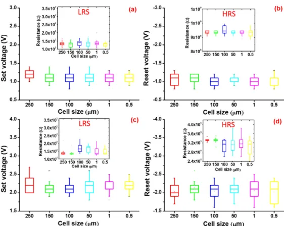
more details, the device is scaled horizontally and vertically. Figures 2.5(a) and 5(b) show that PVD CeOx RRAMs have area-independent set and reset
voltages as device scaled down from 250 µ to 500 nm. Figures 2.4(c) and 4(d) also show that MBE CeOx RRAMs have the similar area- independent
set and reset voltages. Although further scaling of CeOx RRAM needs to be
done for building arrays, Figures 2.5(a)2.5(d) show that Al/CeOx/Au system
has decent scalability in size. The set and reset voltage do not scale down while the size of device shrinks and resistance values at the HRS and LRS can retain at the same order while the device scales down. In addition, horizon-tal scaling results also indicate that the interfacial oxidation and reduction in
our Al/CeOx/Au system are excluded from possible mechanism since the set
and reset voltage are independent to the area of device. For vertical scaling, Figures 2.5(a) and 2.5(b) show that the forming voltage increases when thick-ness of CeOx increases in both MBE and PVD films; this thickness dependent
behavior has been observed in other filamentary path type RRAM devices. Chen[39] proposed a first-order model based on probability analysis showing that thickness scaling would change the forming voltage since the forming is a random process in filamentary path type RRAMs. On the other hand, set and reset voltage are independent to thickness of CeOx film because set and reset
process are local formation and rupture of the filament in switching materials, it requires less energy to eliminate or generate oxygen vacancies compared to forming process.[18] Figures 2.5(c) and 2.5(d) show that Al/CeOx/Au system
with both MBE and PVD films has thickness independent behaviors and this makes the system promising for building extremely scaled devices.
2.4
Conclusion
Resistive switching random access memory devices based on Al/CeOx/Au
sandwiched structure are fabricated by molecular beam epitaxy and electron beam evaporation and demonstrate low set and reset voltage, large operation window (MBE grown CeOx RRAM is larger than 106), stable scalability, and good reliability. Cerium oxide is as favorable as other high-k dielectric ma-terials and should receive more attention for further research and advanced applications such as neuromorphic computing. Besides, based on experiments
Figure 2.4: (a) HRS and LRS resistance along with switch cycles. The struc-ture of tested device is 30 nm Al/13 nm PVD grown CeOx/30 nm Au at room
temperature. (b) HRS and LRS resistance under a continuous 300-mV read voltage. The structure of tested device is 30 nm Al/13nm PVD grown CeOx/
30 nm Au at room temperature and 150◦C. The voltage sweep followed the numerical order in Fig. 2.2(a) for each cycle. Step 1: voltage ramps up to 2.5 V. Step 2: voltage ramps down to 0V, after this half cycle, voltage ramps up to 300mV to read and records the resistance. Step 3: voltage ramps up to -2.2 V. Step 4: voltage ramps down to 0V. Then, voltage ramps up to read and records the resistance.
performed in the chapter, conductive filament path formation and rupture seem more reasonable than interfacial oxidation/reduction.
Figure 2.5: (a) and (b) Diameter of device versus set voltage and reset voltage of MBE grown CeOx RRAMs. (c) and (d) Diameter versus set voltage and
reset voltage of PVD grown CeOx RRAMs. For each area value, 20 devices
have been tested. Inset graphs in (a) and (b) represent the LRS and HRS resistance dependence of MBE devices and inset graphs in (c) and (d) represent the LRS and HRS resistance dependence of PVD devices.
Figure 2.6: (a) and (b) Switching layer thickness dependence of forming voltage with MBE and PVD grown thin film. (c) and (d) Set voltage is independent of CeOx film thickness for both MBE and PVD CeOx film. For each thickness
Chapter 3
Bilayer Cerium Oxide RRAM
3.1
Introduction
Nanoscale metal oxide RRAM have potential in the development of brain-inspired computing systems that are scalable and efficient. In the field of neuromorphic computing, RRAM is also referred as memristor, the cir-cuit element predicted by Chua [26] and found by Hewlett Packard Labs. In Chua’s work [3], biological synapses can be treated as memristor because those synapses have dc current-voltage characteristics matching the definition of generic memristors. That is, dc current-voltage characteristics with hys-teresis and it passes the origin. In neuromorphic computing systems, memris-tors represent the native electronic analogues of the biological synapses. This demonstration is an important step towards the physical construction of high density and high connectivity neural networks. A memristor is a two-terminal memory resistor electronic device, in which a metal oxide switching layer is sandwiched between two metal electrodes [40–43]. In general, memristors offer non-linear switching characteristics, and materials and process compatibility with advanced silicon manufacturing. These attributes have spurred the ex-ploration of memristors as synaptic devices for realizing spike-based hardware learning systems that are capable of processing unstructured, temporal data
[2, 44–47]. However, for memristor-based technologies to be viable, the device should exhibit several key characteristics. It should have a compact nanoscale footprint, operate at a voltage close to 1V that is compatible with comple-mentary metal oxide semiconductor (CMOS) technology, have reproducible electrical characteristics, and possess high switching speed to minimize the energy consumption [42]. Furthermore, the hardware integration of synaptic connections in advanced neural networks requires memristors with multiple re-sistive states [48, 49]. These are challenging requirements and are difficult to implement without significant innovations. The phenomenological principle of memristor device operation is based on the change in the physical properties of a conductive filament (associated with the presence of oxygen vacancies) by applying an electric field across the metal oxide switching layer [50, 51]. The resulting motion of the oxygen vacancies alters the device resistance be-tween low (Set) and high (Reset) states, depending on the direction and the amplitude of the electric field. So far, a variety of structures from a large set of materials (various combinations of metal oxide switching layers and metal electrodes) have been studied in the literature [9]. Several key findings can be drawn from those studies regarding the performance, energy and scalability of this type of devices. The most important finding reveals the trade-off between the switching energy and the data retention time, that is often referred to as voltage-time dilemma[52]. This trade-off is associated with the energy barrier of the device structure.
(Eg), such as titanium oxide (TiOx, Eg∼3.4eV), generally exhibit low
operat-ing voltage and compromised data retention, while those with large bandgap, such as hafnium oxide (HfOx, Eg∼5.4eV) demonstrate the opposite [53].
How-ever, the fabrication of devices with bilayer switching stacks has shown to be effective in mitigating this trade-off. In particular, the improvement in data retention was obtained by the incorporation of an ultra-thin wide bandgap metal oxide capping layer (for example aluminum oxide) [54]. On the other hand, the addition of a reactive capping metal (for example titanium, hafnium, etc.) as an oxygen scavenging layer provided a pathway for reducing the op-erating voltage of the devices [39, 55]. Despite significant advances, a sub-1V memristive device that simultaneously affords built-in analog behavior, en-ergy efficiency on par with a biological synapse, forming-free operation and low device-to-device variations is still elusive.
The cerium oxide RRAM device shows decent operating voltage, fast speed, reliable switching and high operating window; however, it doesn’t demonstrate prominent analog behaviors when it resets. In order to improve analog switching and realize multiple states, an ultra-thin, non-stoichiometric HfOx is added into device stack. In this chapter cerium oxide based
bi-layer memristors that is forming-free, low-voltage (|0.8V|), energy-efficient (full On/Off switching at 2pJ, intermediate states switching at fJ), and reliable are shown. Furthermore, pulse measurements reveal the analog nature of the memristive device; that is it can be directly programmed to intermediate re-sistance states. Leveraging this finding, the device stack demonstrate
spike-timing-dependent plasticity (STDP), a spike-based Hebbian learning rule. In those experiments, the memristor exhibits a marked change in the normalized synaptic strength (>30 times) when the pre- and post-synaptic neural spikes overlap.
3.2
Hafnium Oxide and Cerium Oxide Stacked
Resis-tive Random Access Memory
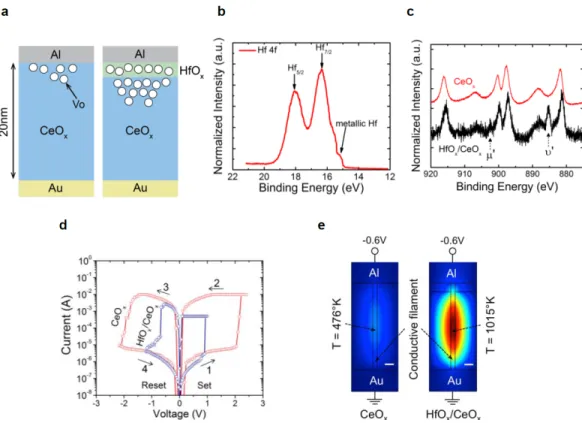
With memristive-based synaptic device by engineering the material properties of an HfOx capping layer in a bilayer structure with a cerium
ox-ide (CeOx) switching layer, the combination of sub-stoichiometric structural
properties of the HfOx capping layer and its enhanced thermal resistivity at
nanoscale dimensions leads to the significant improvement in switching be-havior of the devices in terms of the operating voltages, device performance uniformity, reproducibility, and reliability . Furthermore, this structure yields forming-free devices with an analog resistance state that is inherent to the device itself. This key attribute of our HfOx/CeOx devices enables the
imple-mentation of Hebbian learning [56], validating the plasticity of the synaptic connection. Memristor devices (150µm diameter) were fabricated on silicon substrates capped with 300nm silicon dioxide. The device structure consists of gold bottom electrode, HfOx/CeOx switching layer, and aluminum top
elec-trode. The total thickness of the bilayer switching layer in all experiments was kept at 20nm, while varying the thickness of individual the HfOx and CeOx
Figure 3.1(a) conceptually illustrates the effect of the engineered HfOx
cap-ping layer on the concentration of oxygen vacancies in the CeOx switching
layer. X-ray photoelectron spectroscopy (XPS) was performed to guide the development of the bilayer structure. Figure 3.1(b) shows the Hf 4f spectrum of the engineered HfOx capping layer, revealing the sub-stoichiometric nature
of the film. The data indicates the presence of Hf 4f7/2 and Hf 4f5/2 peaks at 16.32eV and 18.03eV, respectively, which is consistent with the previous reports in the literature [57, 58]. Metallic Hf was also found in the engineered HfOx layer, evident from the peak at 15.02 eV. The chemical composition of
the HfOx was quantified using the CasaXPS software, in which x was found
to be about 1.75. Figure 3.1(c) shows the Ce 3d XPS spectra of the CeOx
switching layer with and without the engineered HfOx capping layer. In these experiments, the CeOx and HfOx layers were 20nm and 0.8nm, respectively.
The thickness of HfOx was chosen so that it allowed X-ray beam to penetrate
into underneath CeOx layer and received decent signal strength. As a result,
the adequately small thickness of the HfOx capping layer allowed the XPS
an-alyzer to receive signal from the CeOx layer. As can be seen in Figure 3.1(c),
the bilayer structure exhibits discernable u0 and v0 peaks at 904 eV and 885 eV [35, 36, 59] that are absent in the spectrum of the CeOx layer with no
HfOx capping layer. The u0 and v0 peaks signals the reduction of the Ce4+
to Ce3+ states, which can be translated to the formation of excess oxygen vacancies at regions near the HfOx/CeOx interface. The marked increase of
forma-tion of the conductive filament using a smaller electric field, thereby enabling the low-voltage operation of the bilayer structure. Figure 3.1(d) shows the representative dc current-voltage characteristics of two CeOx-based devices
with and without the engineered HfOx capping layer, demonstrating
signifi-cant reduction of the Set voltage to below 0.8V. In a memristive device, the transition from low to high resistance states occurs as the polarity of the elec-tric field across the device is reversed. As the reverse elecelec-tric field increases, the oxygen anions in the conductive filament begin to disperse through drift and diffusion processes [47]. Considering the similar thickness of the switching layer in Figure 3.1(d), the improved Reset voltage of the bilayer device may be explained by locally enhanced diffusion of oxygen vacancies. We infer that the enhanced thermal resistivity of HfOx at nanoscale dimensions amplifies
Joule heating in the CeOx switching layer, thereby accelerating the
disper-sion of oxygen anions at a lower electric field. To elucidate this concept, we performed numerical heat transfer analysis using COMSOL simulator for two devices in Figure 3.1(e) at the bias of -0.6V. The simulation results indicate significant enhancement of Joule heating in the bilayer structure. For these simulations, we used the measured electrical parameters of the layers, while the thermal parameters were obtained from the literature[60–63]. The fabri-cation procees is as follows: CeOx layer was reactively evaporated in oxygen
plasma ambient at 0.2mTorr and an average deposition rate of 0.06nm/s. The HfOx layer was formed by plasma-assisted atomic layer deposition (PE-ALD)