c
DISTRIBUTED GRID ANALYTICS PLATFORM (DGAP) FOR POWER GRID MONITORING
AT THE DISTRIBUTION LEVEL
BY YUQI LI
THESIS
Submitted in partial fulfillment of the requirements
for the degree of Master of Science in Electrical and Computer Engineering in the Graduate College of the
University of Illinois at Urbana-Champaign, 2015
Urbana, Illinois Adviser:
ABSTRACT
Phasor measurement units (PMUs) which measure electrical waves with real-time synchronization at widely spread points across the power grid offer great benefits. While the PMU device concept is well known in the power industry, the field of power system analysis stands to benefit greatly from using different methods of designing and implementing an inexpensive PMU that can be widely and densely distributed on the grid. Traditional PMUs are mainly installed at the transmission level, where they are hard to install and maintain, and can be expensive due to the rating requirements of the components. Given their benefits and increasingly widespread installation, easier-to-maintain and less costly PMUs are desired.
In 2000, frequency disturbance recorders (FDRs), which are single-phase PMUs that monitor the power grid at the 120 V distribution level, were operated for the Frequency monitoring Network (FNET) project by Virginia Tech and the University of Tennessee. While installing FDRs at the low-voltage distribution level of the power grid was a great step toward reducing the cost and limitations of PMU use, there are still drawbacks and significant room for improvement: the sampling frequency is low at 1440 samples per second (SPS), there is no auxiliary power supply to support the device during an atypical power grid event, and the USD 2000 price can be driven lower.
This thesis introduces the Distributed Grid Analytics Platform (DGAP) which has a higher sampling rate (20k SPS), a backup power supply, smaller size, and much lower cost (USD 200) while keeping the functionality of the FDRs including accurate data acquisition, GPS time synchronization, inter-net connectivity, and open source data upload. The improvements were re-alized by a more succinct approach for the system design and more updated component selection, which will be explained in this thesis. The designed
DGAPs were built into prototypes and tested in household power outlets, experimentally validating their functionality.
ACKNOWLEDGMENTS
Thanks to Professor Robert C.N. Pilawa-Podgurski, my thesis advisor, for his help and guidance during the past two years. He showed me how to be a professional and serious researcher and prepared me to enter the industrial world. I am grateful for the opportunity to learn from him not only as a great researcher but also as a great person in other aspects: I enjoyed his power electronics classes in which he always presented the contents in a practical but interesting way, and I received great advice from him throughout my graduate school and future planning, without which my career path could be very different.
Thanks to Andrew R. Stillwell for spending much of his precious time on my project. The work in this thesis would not be possible without his tremen-dous help. His industrial background and insight into micro-controllers were momentous to the success of the project. Many people helped me a lot with the work in this thesis. Christopher Drew helped looking into data transfer between C and Python as well as data upload to Open PDC. Mark Hirs-brunner coded the internet connection of Beaglebone. Rodrigo Serna and Jingyi Ma helped experimenting with ADC and GPS. Thanks to my fellow researchers in the research group, Christopher Barth, Enver Candan, Yu-tian Lei, Benjamin Macy, Shibin Qin, Joshua Sheridan, and many more, for sharing their knowledge and all their help.
Thanks to Professor Thomas J. Overbye for funding my project through the Illinois Center for a Smarter Electric Grid (ICSEG).
Thanks to those who have accompanied me throughout graduate school, especially to Yujia Zhang, the other girl in my power electronics lab during my first year, who has been my partner for so many lab courses as well as
for lunches; Di Fan, who has been like a sister to me, has great taste in life and great interest in burning money with me; and Jianan Wang, who almost did not make it into these acknowledgments since he showed up so late in my life, but thankfully he finally came.
Most of all, thanks to my parents for their support. Even though they are not near by my side most of the time, their help and love were a great comfort in my endeavors.
TABLE OF CONTENTS
LIST OF TABLES . . . ix
LIST OF FIGURES . . . x
CHAPTER 1 INTRODUCTION . . . 1
1.1 Introduction . . . 1
1.2 Organization of this Thesis . . . 3
CHAPTER 2 HARDWARE IMPLEMENTATION . . . 4
2.1 System Level Structure . . . 4
2.2 Component Selection . . . 7
2.3 Prototypes . . . 22
CHAPTER 3 SOFTWARE IMPLEMENTATION . . . 25
3.1 Software Work-flow . . . 25
3.2 Mathematical Methods for RMS Voltage, Frequency, and Phase Calculation . . . 26
CHAPTER 4 EXPERIMENTAL RESULTS . . . 30
4.1 Testing Setup . . . 30
4.2 Test with Controllable AC Power Source . . . 32
APPENDIX A SCHEMATIC DRAWING FOR DGAP REV 2.0 . . . 37 APPENDIX B PCB LAYOUT FOR DGAP REV 2.0 . . . 40 APPENDIX C PROTOTYPE PHOTOS FOR DGAP REV 2.0 . . . 46 APPENDIX D COMPONENT LISTING FOR DGAP REV 2.0 . . . 51 APPENDIX E EXPERIMENTAL DATA FOR DGAP REV 2.0 . . . 53 APPENDIX F DGAP CODE IMPLEMENTED IN BEAGLEBONE
BLACK . . . 56 F.1 Assembly Code for Programmable Real-time Unit . . . 56 F.2 C Code for PRU Initialization and Data Transfer Between
Shared Memory and Python Code . . . 65 F.3 Python Code in ARM CPU . . . 75 REFERENCES . . . 84
LIST OF TABLES
2.1 Polymer Li-Ion Cell Features [1] . . . 11 2.2 LP2985-33DBVR Features [2] . . . 13 D.1 Component List for the Distributed Grid Analytics Platform . 52 E.1 Frequency Measurements and Reading Error . . . 54 E.2 Vrms Measurements and Reading Error . . . 55
LIST OF FIGURES
2.1 DGAP hardware structure at the system level. . . 4
2.2 The voltage-step-down circuit. . . 5
2.3 Top view of Beaglebone Black. . . 7
2.4 AM335x functional block diagram adapted from [3]. . . 8
2.5 Top view of Adafruit Ultimate GPS Breakout. . . 9
2.6 Serial data output of the GPS. . . 10
2.7 Diagram of how GPS data contribute to accurate time-stamps. 10 2.8 Connection of MCP73811 for charging rate of 450 mA. . . 12
2.9 Connection of LP2985-33DBVR. . . 14
2.10 Connection of ADC141S626. . . 16
2.11 Channel directions of ADuM640x series adapted from [4]. . . . 17
2.12 Pin configuration of ADuM6401. . . 18
2.13 Regions hollowed out on the box for connectors and LEDs. Front view (top) side view (bottom). . . 21
2.14 Distributed Grid Analytics Platform Rev. 2.0. . . 22
2.15 Distributed Grid Analytics Platform Rev. 1.0. . . 23
3.1 Software work-flow of the FDR. . . 25
3.3 FFT of since wave with integer number of cycles (left) and
non-integer number of cycles (right). . . 28
4.1 Bench setup for DGAP testing. . . 30
4.2 PMU Connection Tester workspace (120 Vrms 60 Hz). . . 32
4.3 PMU Connection Tester workspace (120 Vrms 59 Hz). . . 33
4.4 PMU Connection Tester workspace (120 Vrms 61 Hz). . . 33
4.5 PMU Connection Tester workspace (120 Vrms, 61 Hz to 60.5 Hz). . . 34
4.6 Percentage error vs. frequency. . . 35
4.7 PMU Connection Tester workspace (wall outlet). . . 36
A.1 Low voltage region of the DGAP. . . 38
A.2 High voltage region of the DGAP. . . 39
B.1 PCB layout top view. . . 41
B.2 PCB layout bottom view. . . 42
B.3 Top silkscreen. . . 43
B.4 Top-layer copper. . . 44
B.5 Bottom-layer copper. . . 45
C.1 Top view of the fully assembled DGAP. . . 46
C.2 Front view of the fully assembled DGAP. . . 47
C.3 Side view of the fully assembled DGAP. . . 47
C.4 Top view of the board without BBB. . . 48
C.5 Bottom view of the board without BBB. . . 48 C.6 Top view of the board with BBB and external antenna attached. 49
C.7 Front view of the board with BBB and external antenna
attached. . . 49 C.8 Side view of the board with BBB and external antenna attached. 50 C.9 Rear view of the board with BBB and external antenna
CHAPTER 1
INTRODUCTION
1.1
Introduction
Phasor measurement units (PMU) have been playing an important role in power grid monitoring. A PMU is a device that measures the voltage and current on an electricity grid and obtains the frequency and phase data from the voltage and current data measured [5]. The PMUs are also time synchro-nized, which enables synchronized real-time measurements of wide ranging measurement points on the grid [6]. With continuous sampled and synchro-nized real-time data from different locations, the data are widely used for power system model verification. More importantly, PMUs can be used to perform real-time power grid monitoring; if incorporated with relays and other circuit protective devices [7], the device can trip the grid to prevent damage before things happen [8]. From this real-time monitoring aspect, the data collected around an atypical event can be studied for power system behavior analysis and contribute to future power grid technologies [9]. Due to all the benefits a PMU can provide, they are considered one of the most important measuring devices in the future of power systems [10].
As technology has evolved, PMUs have evolved significantly as well [11]. Traditional PMUs are usually installed on transmission lines with voltage up to 765 kV. This PMU is very expensive because it must operate safely in a high voltage environment; in addition, installing a device on the transmis-sion line can be expensive and time-consuming, costing tens of thousands of dollars per device and requiring several months of effort. Maintaining the device can also be costly. These constraints limit the number of PMUs we can distribute to the field and, thus, their use in the electric power industry.
In 2000, Frequency Disturbance Recorders (FDRs), which are PMUs that can be installed at the low-voltage distribution level of the power grid [12], were introduced. Since voltages involved are much lower than those for tra-ditional PMUs, FDRs are relatively inexpensive and simple to install. FDRs sample at 1440 samples per second and transmit to the Frequency monitor-ing Network (FNET) for processmonitor-ing and storage. As the distribution-level FDRs have been developed, the number of deployed PMUs has significantly increased.
As time goes on, it seems that we always need PMUs to be distributed more densely and sample data faster. That is why Distributed Grid Analytics Platforms (DGAPs) have been developed. DGAPs aim to sample faster and operate more reliably while costing less. DGAPs have been developed and the prototypes are tested and ready for deployment in the field. The cost per DGAP is estimated to be under 200 USD, one tenth that of FDRs. The DGAP is implemented with backup battery power supply, so it can capture data even when the voltage at the power grid is too low to support the device. The DGAP samples data at 20k Hz, which capture more transient behavior of the power grid. The data collected by DGAP — the time-synchronized rms voltage, frequency, and phase data — can be used to do event detection and location estimation [13], power system event visualization, power grid oscillation detection [14], on-line trip detection, off grid/islanding detection [15], and all other power system research. As the data is more transient and more reliable, it could help advance power system research to a new future, especially when renewable energy sources such as solar power come into play [16] and more transient and accurate monitoring are needed.
The upper level description of how the DGAP works is as follows. The DGAP samples a scaled-down version of the power outlet’s voltage signal using an analog-to-digital converter, and these data are processed to a micro-controller for further calculations. Each measurement is time stamped with time information provided by a GPS, and then all those data are transmitted to a server for processing and storage. More detailed explanations will be presented in this thesis.
1.2
Organization of this Thesis
This remainder of thesis is divided into three chapters.
Chapter 2 introduces the design and implementation of the DGAP hard-ware. Considerations during system design and component selections are described in detail. Advantages and possible future improvements of each component are highlighted. These prototypes are used for all the software design and experimental testing explained in the following chapters.
Chapter 3 explains the software structure of DGAP and mathematical implementations for obtaining RMS voltage, frequency, and phase data.
Chapter 4 presents the test setup and experiments performed to verify the functionality of the DGAP prototypes. Obtained data are analyzed, and future efforts of what need to be improved are discussed.
CHAPTER 2
HARDWARE IMPLEMENTATION
In this chapter, the design and implementation of the DGAP hardware are introduced. Considerations during system design and component selections are described in detail. Future improvements that can be done are stated in each section.
2.1
System Level Structure
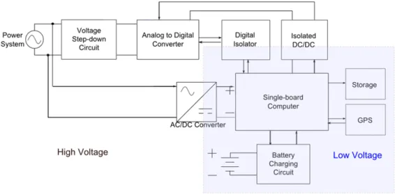
The system level hardware structure of the DGAP is shown in Fig. 2.1
Figure 2.1: DGAP hardware structure at the system level.
The “Power System”terminal represents the 120 Vrms AC power outlet. From the power outlet, the wire goes in two directions: one goes to the data acquiring system, and the other provides power to the device.
At the beginning of the data acquiring system, the 120 Vrms AC voltage feeds into a voltage-step-down circuit through an AC power connector [17]. The voltage-step-down circuit converts the 120 Vrms AC voltage, which is in the range of±170 V, to the range of 0 V to 3.3 V. This step is essential since most analog-to-digital converters (ADCs) only take positive analog voltage input under 5 V. The reason we step down the voltage even further to limit the maxim input value to 3.3 V is that the device is operating on a 5 V power rail, thus the reference voltage provided to the ADC cannot reach 5 V, which places an upper limit of the input voltage; this choice of values will be explained in detail in Section 2.2. The voltage-step-down circuit is shown in Fig. 2.2.
Figure 2.2: The voltage-step-down circuit.
At the input of the voltage-step-down circuit, an input range of ±185 V was used instead of the±170 V, which is ±120×√2 V, to allow some room for disturbance and abnormal performance of the power grid; the output of the circuit ranged from 0.1 V to 3.2 V instead of 0 V to 3.3 V for the same purpose. With this setup, the relationship between input and output can be defined as
output= 3.2V, when input= 185 V
output= 0.1V, when input=−185 V
(2.1)
circuit, the sum of currents flowing into that node is equal to the sum of currents flowing out of that node, the circuit can be represented as
3.3 V−3.2 V R2 + 185 V−3.2 V R1 = 3.2 V R3 3.3 V−0.1V R2 + −185 V−0.1V R1 = 0.1 V R3 (2.2)
By solving Equation. 2.2, the ratio of R1, R2, and R3 was obtained to be
roughly 58:1:1. The choice of exact values of the resistors will be explained in Section 2.2.7.
The stepped-down voltage feeds into the ADC as analog signals, then the ADC outputs digital signals to the micro-controller through a digital isolator. As indicated in Fig. 2.1, there is a high voltage region, which has direct contact to the power outlet, and a low voltage region, which does not touch the 120 Vrms AC voltage at all. The function of the digital isolator is to isolate the high voltage and low voltage region so that if anything abnormal happens at the power grid, or if any component at the high voltage region does not function correctly, the micro-controller does not get burned due to possible overrated voltage or current. The isolated DC/DC in the power path between micro-controller power rail and the ADC serves the same purpose.
From another route, the power outlet feeds into a power adapter which provides 5V DC to the micro-controller, which provides power to the rest of the system. When the power outlet is incapable of providing power to the device, the micro-controller starts drawing power from an external battery through the battery charging circuit; once the device start drawing power from the power outlet, the battery charging circuit charges the rechargeable battery for future use.
A GPS is built in for real-time stamps and synchronization. The micro-controller is connected to internet via Ethernet for data upload. When the device temporarily loses internet connection, a single 256Mb x16 DDR3L 4GB (512MB) memory on the single-board computer will be used for data storage.
2.2
Component Selection
This section explains how the components in the system are selected. A list of components mentioned in this section can be found in Table D.1 within Appendix D.
2.2.1
Single-board Computer
When it comes to choosing what single-board computer to use, there are several different aspect to be considered and several functionalities to be fulfilled.
The single-board computer needs to have a micro-controller that can per-form real-time data sampling at a high enough rate as well as efficiently analyze the acquired data mathematically. It needs to have output power rails to power the rest of the system. It has to have two or more communica-tion interfaces to communicate with peripheral components such as GPS and ADC. It needs to have internet access through Ethernet or wi-fi or some other kind for data sharing. It needs to have some kind of data storage to store data temporarily. And also, since one of the goals of this DGAP is to make it as inexpensive as possible, it should be open-sourced with a reasonable price.
Beaglebone Black (BBB), as shown in Fig. 2.3, is one single-board com-puter which fulfills the listed requirements.
The functional block diagram of the Sitara XAM3359AZCZ100 Processor on board is shown in Fig. 2.4.
Figure 2.4: AM335x functional block diagram adapted from [3]. The ARM Cortex-A8 CPU in the Sitara Processor operates in a Linux system. There are two images to choose from, Debian and Angstrom. Our project used Debian because it has a wider support. All the data analysis can be performed in this ARM CPU. The problem is that Linux lacks a real-time system to sample data deterministically, and it has a slow I/O, around 10kHz, which is not fast enough for our target data sampling rate. Fortunately, there is a programmable real-time unit (PRU) on the Sitara Processor which can fill in these gaps. The PRU samples data with accurate time stamps, disregards any interrupts from background or elsewhere, and can run at 200 MHz, which is fast enough for our device. The only minor disadvantage of this setup is that the PRU is coded in Assembly, which could make it a little bit harder to perform fancier functionalities. There is 64K shared RAM which both the ARM and PRU can access; thus after the PRU
samples the data at an accurate time stamp, it exports the data to the shared RAM, and then the ARM processor takes the data over for further analysis. Duo CPU also gets the work done faster, which can be critical in the future as we raise the sampling rate further.
For communication interface, the Sitara processor has 6 universal asyn-chronous receiver/transmitter (UART) interfaces, 2 serial peripheral Inter-faces (SPIs), and 3 I2C interfaces, which leaves plenty of space for choosing
peripheral components that use communication interfaces. It has a single 256Mb x16 DDR3L 4Gb memory device on board for temporary data stor-age when necessary.
For internet, the Beaglebone can use either the Ethernet cable or a USB wi-fi dongle. For battery, Beaglebone has pulled out battery connection pins as TP5 - TP8 for external battery system connections.
Other than having all the required functionalities, what makes Beaglebone Black stand out from other single-board computers is that both the hardware and software of BBB are open-sourced, which means the schematics and PCB layouts are all available if any modification to the hardware needs to be done.
2.2.2
GPS
The Adafruit Ultimate GPS Breakout, shown in Fig. 2.5, was selected.
Figure 2.5: Top view of Adafruit Ultimate GPS Breakout.
This GPS board is built around the FGPMMOPA6H MT3339 GPS mod-ule. This module is 5 V friendly and ideally has a 20 mA current draw.
This GPS has a UART interface to communicate with the micro-controller (trough pin TX and RX) for time and location information as shown in Fig. 2.6, and also a pulse per second (PPS) output which can be used for time synchronization. Fig. 2.6 shows a series of sample output data from the GPS which are transferred to the micro-controller through UART. The six-digit number right after the “GPRMC” (recommended minimum specific GPS/Transit data) is the “hhmmss” used for time information [18].
Figure 2.6: Serial data output of the GPS.
Fig. 2.7 shows the time relationship between the PPS signal and the serial data. The pulse signals the start of a second, then all the data sampled within this second is stamped by the time information acquired through UART. Since the device desires to output 20 data per second, it will rely on the system clock to divide one second into 20 pieces. The resulting time portion of the final output data of the device is shown in Fig. 2.7.
Figure 2.7: Diagram of how GPS data contribute to accurate time-stamps. Considering that the in-doors usually has very poor satellite reception for
GPS, the Adafruit Ultimate GPS Breakout also has a uFL connector built in for an external active antenna. For the DGAP, an external active antenna with a 5 meter long cable is selected so the antenna can reach out of a window for better satellite reception. There is a “FIX” output that can be connected to an external LED to indicate if the GPS is getting satellite. This signal will be pulled high every second if there is no satellite reception, and will be pulled high every 15 seconds for good satellite reception.
The module can be enabled or disabled easily by pulling the “EN” pin.
2.2.3
Charge Management IC and Li-ion Battery
The backup power supply system is composed of a charge management IC and a battery. This subsystem is connected to Beaglebone Black at pins TP5-TP8, which are presented as a 2x2 header right under the 5 V DC input jack.
By lab observation of DGAP Prototype Version 1.0, the DGAP could draw up to 500 mA current with 5 V DC input but never exceed this amount. A Li-ion battery with features listed in Table 2.1 was selected. The battery can continuously provide 500 mA current to the device and can output 1 A for a short period of time if any unusual power withdrawal occurs.
Table 2.1: Polymer Li-Ion Cell Features [1] Nominal Capacity 500mAh 1.85Wh Charging rate 0.5A Max. (1.0C rate) Continuous Discharging Rate Continuous: 0.5A (1C) Max Discharging Rate 1A (2C) for 30 second
Ideally the four pads TP5-TP8 are provided to allow access to the battery pins on the built-in single-chip PMIC TPS65217 which perform the charge and discharge of the battery power; however, during testing, the PMIC was able to discharge the battery to provide power to the system, but was un-able to charge the battery when external USB or DC power is present. Thus
charge management IC was needed to perform battery charging. Consider-ing the battery’s maxim chargConsider-ing rate is 500 mA, MCP73811, which has a selectable charge current of 85 mA/450 mA [19], was selected for battery charge management. Even though TPS65217 on board is not performing the battery charging alone, the battery charging circuit is still connected to Bea-glebone through the four pads which are connected to TPS65217, thus the max output current of the TPS65217 was checked to make sure the charging current does not exceed the PMIC’s maxim charging current, which is 1.2 A. For a charging rate of 450 mA, which is the application in our device, the PMIC chip is connected as shown in Fig. 2.8; in the future, if withdrawing 450 mA becomes too much for Beaglebone Black to handle, pin 5 can be grounded to select a charging rate of 85 mA.
Figure 2.8: Connection of MCP73811 for charging rate of 450 mA. TP7 on BBB was left floating since the temperature sensor input is not necessary in our case. Note that if the BBB is running off the battery power, the system voltage pins will output 3.3 V instead of 5 V, which is the voltage when BBB is running off the external USB or DC jack.
During prototype testing it was found that if the device is powered from the 5 V DC power jack, when the power is removed, BBB turns off regardless of the present of the battery; but if the device is powered from USB, the BBB keeps functioning with power provided by the battery. Then it was found that, given how the BBB is implemented, if the present 5 V DC power is removed, the power pin to the ARM will be toggled and power down. Thus for the device to smoothly transfer from external power to battery power when needed, the power needs to be provided from USB, but not the 5 V DC power jack.
2.2.4
Linear Regulator
The linear regulator in the device will contribute two parts: the reference voltage of the ADC and the reference voltage Vref in the voltage-step-down
circuit. Typically most linear regulators provide output voltage of 1.8 V, 2.5 V, 2.8 V, 2.9 V, 3.0 V, 3.1 V, 3.3 V, 5.0 V, and 10 V to choose from. We want the output voltage of the linear regulator to be as high as possible because a high reference voltage gives the ADC a wider input range, greater value per bit, and thus better accuracy; but since the Beaglebone Black outputs 5 V through the power isolator to the components on the high voltage side, the value of the linear regulator is limited. The linear regulator with 5.0 V could be the best choice if it is guaranteed that the power isolator always provides
≥5 V to theVin of the linear regulator, but because there can be disturbance
and voltage drop from the power isolator or other cause from the system, the 3.3 V is selected to be safe. Since the DGAP has an accuracy standard to meet, we want the selected chip to have low output tolerance, low dropout, and low noise. After comparisons, LP2985-33DBVR with features shown in Table 2.2 was chosen.
Table 2.2: LP2985-33DBVR Features [2] Output tolerance (Standard Grade) 1.5%
Dropout rate 280 mV at 150 mA
7 mV at 1 mA Noise (with 10-nF Bypass Capacitor) 30µVRM S
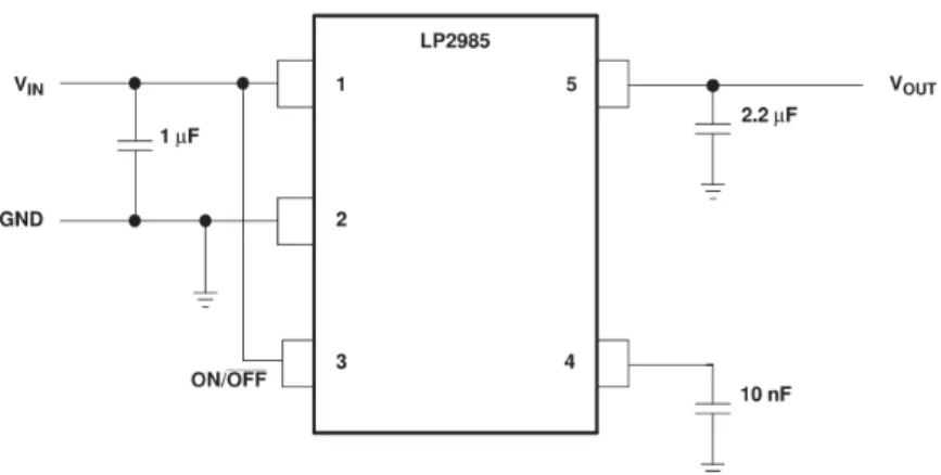
LP2985-33DBVR has a relatively low output tolerance, low dropout, and low noise compared to a selection of other linear regulators and requires fewer external components. The external capacitors are connected as shown in Fig. 2.9 for low-noise operation and output stability. The enable pin (pin 5) is directly connected to high since the output of the linear regulator is constantly needed.
Figure 2.9: Connection of LP2985-33DBVR.
2.2.5
Analog to Digital Converter
The analog-to-digital converter (ADC) takes in a voltage reading between 0 V and the Vref which is 3 V, and outputs a series of digital signals which can
be read by the micro-controller. The analog value for the least significant bit (LSB) of the serial of digital signal can be calculated as
LSB = Vref
2#bits−1 (2.3)
For example, there is a 12-bit built-in ADC in the Sitara processor, so if we use a reference voltage of 3.3 V, the value of the LSB of this particular ADC is
LSB = 3.3 V
212−1 '0.8059 mV (2.4)
Therefore, if the micro-controller reads 2310 from this ADC, for example, the voltage at the input of the ADC can be calculated as
V = 0.8059 mV ×2310 = 1.8615 V (2.5) The value of the LSB is one factor that determines how accurate the ADC reading can be. An ADC with LSB = 0.8059 mV means the voltage read can
only increment by 0.8059 mV, thus it will not reflect the voltage accurately if the voltage variation is less than 0.8059 mV. Decreasing the value of the LSB increases the accuracy of ADC reading. Also notice that the voltage the ADC reads is scaled down from ±185V to 0.1 V to 3.2 V, thus the error will be even larger after the 1.8615 V is transformed back to the full scale. From this aspect, the 12-bit ADC on Beaglebone Black could be too inaccurate to be used in the DGAP to meet the IEEE standard [20].
A 14-bit ADC ADC141S626 was used in the device. As ADC141S626 takes both positive and negative voltage inputs, which is very different from many other ADCs, and its most significant bit (MSB) presents the sign of the voltage input [21], it is thus really a 13 bit ADC with input voltage that is twice wider. Prototype Version 2.0 only used the positive part of the input, which can be improved in the future with some modification of the voltage-scale-down circuit. For Prototype Version 2.0, the value of the LSB of ADC141S626 is
LSB = 3.3 V
213−1 '0.4029 mV (2.6)
The voltage at the power outlet (V1) and the voltage at the input of the
ADC (V2) can be described by a linear equation V1 =aV2+b. To scale back
the voltage reading, we know −185 = 0.1a+b 185 = 3.2a+b (2.7)
Solving Equation 2.7, we get a'119.36, b' −196.94, thus
V1 = 119.36V2−196.94 (2.8)
which means the measured voltage value increments by
This value will be halved if the negative portion of the input range is also used. The real value could be off by a little bit due to the tolerances of the components such as the resistors in the voltage-scale-down circuit, the linear regulator output voltage, etc., thus calibration is needed before put the device in field.
ADC141S626 has a maxim sampling rate of 250 kSPS, which is more than enough to provide our desired 10 kSPS sampling rate. It uses the SPI com-munication interface which is supported by Beaglebone Black. It takes the system clock (SCLK) and chip selection (CS) signals, which determine the sampling rate, from Beaglebone Black and feeds back sampled data Dout.
The external capacitors are connected as shown in Fig. 2.10 for low-noise operation and input stability.
Figure 2.10: Connection of ADC141S626.
2.2.6
Digital & Power Isolators
Digital and power isolators are used between BBB and all the components on the high voltage side, including the ADC and the linear regulator, to isolate any signal and power route. This measure can be very beneficial from the safety aspect; it protects the system on the low voltage side (including the Beaglebone Black, the GPS, the backup battery system) from abnormal current or voltage caused by fault in the power grid or broken parts in the high voltage side which may damage components in the low voltage part or cause safety hazards.
There are many isolators to choose from. For the DGAP, there are 3 signals to be isolated between BBB and the ADC: from BBB to ADC, we have system clock and the chip selection signal; from ADC to the BBB, there is the sampled data. And the BBB needs to provide power to ADC and the linear regulator through a power isolator. The ADuM640x series stands out since it includes the signal isolation channels and power isolator in one single chip. The power isolator can take 5 V or 3.3 V input from the BBB and output 5 V or 3.3 V to the high voltage side, which means even if the BBB is running off the battery power, the system on the high voltage side can still have 5V power rail. The power isolator can output up to 400 mW, which is capable of supporting the high voltage side. As a signal isolator, ADuM640x has four channels; the difference between ADuM6400, ADuM6401, ADuM6402, ADuM6403, and ADuM6404 is the direction of the channels, as shown in Fig. 2.11.
Figure 2.11: Channel directions of ADuM640x series adapted from [4]. The DGAP requires two signal channels in the same direction as the power channel, and one signal channel in the opposite direction; thus both ADuM6401 and ADuM6402 would work, and ADuM6401 was chosen. The pin configuration of ADuM6401 is shown in Fig. 2.12. VDDL (pin 7) is
con-nected to VDD1 (pin 1) to supply power to the data channels, and VSEL (pin
10) is connected to VISO (pin 16) to select 5 V output voltage (VISO = 5V). From the data sheet, it was noted that 5 V output with a 3.3 V input is discouraged since this combination has quite low power efficiency. But since power consumption is not a critical consideration in this project at this stage,
Figure 2.12: Pin configuration of ADuM6401. Prototype Version 2.0 is fine with this setting.
2.2.7
Resistors in the Voltage-Step-Down Circuit
In Section 2.1, we have discussed the voltage-step-down circuit and obtained the ratio between R1, R2, and R3 from Equation 2.2 to be 58:1:1. When
choosing the value of the resistors, we need to consider both the power rating and the noise. The resistance value can be large to prevent reaching the power ratings, but as the resistance value increases, the noise at the output will increase as well; since data accuracy is critical to a DGAP, we want to keep the resistor values as low as possible.
Most surface mount resistors with unitkωusually have power rating of 1/8 W or higher. According to Fig. 2.2, the maxim voltage that can be applied toR2 orR3 is 3.3 V (disregard the 0.1 V margin). The relationship between
resistance R, voltage V, and power P of a resistor is
P = V
2
R (2.10)
R2,3 =
(3.3 V)2
1/8W = 87.12 Ω (2.11)
The maxim voltage that can be applied to R1 is -185 V (disregard the 0.1
V margin), thus the minimum resistance capable for R1 is
R1 =
(−185V)2
1/8W = 273.8kΩ (2.12)
To keep the ratio of 58:1:1, R1 limits the minimum value of R2 and R3.
R1 = 357kΩ was chosen, thus R2 and R3 supposed to be
R2,3 =
357kΩ
58 = 6.16kΩ (2.13)
To ensure the measurements to be as accurate as possible, resistors with 1% tolerance are desired, and these have a set of standard values. 6.19kΩ is the closet one to the calculated 6.16kΩ [22], thus it is selected.
Most of the resistors on board, includingR2andR3, have the 0603 package.
For R1, referring to Appendix B, we can see that the space between the two
pins of R1 is the only blank between the power outlet and the rest of the
circuits behind R1; thus 1206, a larger package for R1 which gives a larger
space between its two pins, is selected for safety reasons.
2.2.8
Circuit Protection and Signal Indication
As mentioned in Section 2.2.7, the space between the two pins of R1 is the
only gap between the power outlet and the rest of the circuits. Even though we have increased the package size of R1, more safety measures can be
ap-plied. A fuse (250 V /500 mA rating [23]) is inserted between R1 and the
power outlet connector to prevent over current /voltage.
For signal transmission, all the signal routes have a 5Ω series resistor to prevent short circuit. Exceptions include R12 and R13 which are in series
with the LEDs, indicating the presence of Beaglebone’s system voltage (Vsys)
and 5 V external voltage. Since the LEDs indicate power and are directly connected to the power rails without current limitation, R12 andR13need to
be larger to limit the current through the LEDs so it does not go over the limit, which is 30 mA for the LEDs selected [24]. By Ohm’s law, R12 and
R13 need to be at least
R12,13=
5 V
30mA = 166.67 Ω (2.14)
assuming the LED does not have a resistance. 200Ω resistors are selected for
R12 and R13.
2.2.9
Container
A Hammond Project Box with size that will fit the board was chosen. The box has eight stands to screw in the PCB. Holes are hollowed out at the front and side of the box as shown in Fig. 2.13 for the connectors and LEDs.
Figure 2.13: Regions hollowed out on the box for connectors and LEDs. Front view (top) side view (bottom).
2.3
Prototypes
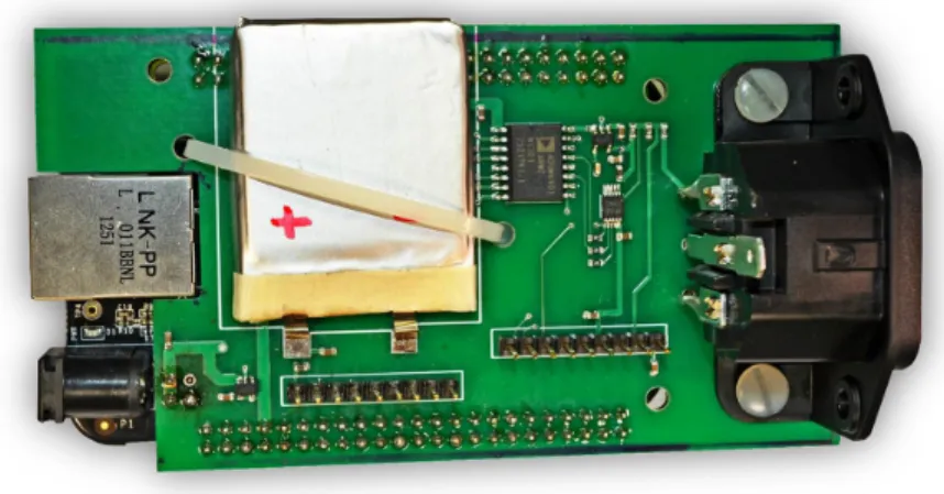
Fig. 2.14 shows the end product. More photos showing the device from multiple views can be found in Appendix C.
Figure 2.14: Distributed Grid Analytics Platform Rev. 2.0.
Compared to DGAP Rev. 1.0 as shown in Fig. 2.15, Rev. 2.0 has more space between the high voltage side and the low voltage side for safety rea-sons.
Figure 2.15: Distributed Grid Analytics Platform Rev. 1.0.
Rev. 2.0 has pulled out Beaglebone system voltage (Vsys), 5 V DC voltage
(VDC), GPS FIX signal (FIX), ADC chip selection (CS), Ethernet enable
(Ethernet), and signal that indicates the presence of the power outlet AC voltage (Vac) to six LEDs on the side edge of the PCB. Vsys indicates that the device is powered. VDC indicates that the device is drawing power from
the external 5 V DC power jack. FIX indicates the GPS satellite reception status, the same pattern as explained in Section 2.2.2. CS indicates that BBB is normally asking ADC to sample data. Vac indicates that the device
is finely plugged into the power outlet.
In the high voltage region of the board, there is a row of headers for testing purposes. Signals pulled out include the 3.3 V reference voltageVref, positive
signal input of ADC (+IN) and negative signal input of ADC (-IN), system voltage (VDD) and Ground (GND) of the high voltage side, chip selection of ADC (CS), serial data output of ADC (DATA), and system clock of BBB (CLK).
At the very middle of the board, there is a 2x2 header (P6). P6 is the battery pads corresponding to TP5-TP8 on Beaglebone black. When assem-bling, after the BBB is secured on the PCB, use wires to connect P6 to TP5 – TP8 on BBB, upper left pin to upper left pin, lower right pin to lower right pin, respectively.
CHAPTER 3
SOFTWARE IMPLEMENTATION
3.1
Software Work-flow
The system level software work-flow for the DGAP is shown in Fig. 3.1
Figure 3.1: Software work-flow of the FDR.
The general idea is as follows. One of the programmable real-time units (PRUs) on board acquires 14 bits raw data from the ADC and transfers it to the shared memory; the other PRU counts the number of micro-controller timebase ticks between pulse per second (PPS) signals from GPS, which will be used for time synchronization. On the other side of the shared memory, the ARM processor will use C code to draw the unscaled raw data and transfer it to Python for further processing. The GPS also provides time information to ARM through UART. After the raw data get scaled and the frequency,
Vrms, and phase are calculated, the data in defined chunk sizes are sent to
an open source PMU data handler called Open PDC through TCP/IP. The Assembly, C and Python code are given in Appendix F.
3.2
Mathematical Methods for RMS Voltage,
Frequency, and Phase Calculation
After the voltage data and the time stamps are all imported to the Python code, different mathematical methods are compared to choose the one that gives the most accurate RMS voltage, frequency, and phase measurements. This section will present the mathematical methods used for data calculation utilized by DGAP.
3.2.1
RMS Voltage Calculation
By definition, the root mean square (RMS) value of a set of values is defined as the square root of the arithmetic mean of the squares of the values as shown in Equation 3.1. xrms = r 1 n(x 2 1+x22+· · ·+x2n) (3.1)
The DGAP calculates Vrms in the exact same way. The device calculates Vrms every 50 ms, with the sampling rate of 20 kSPS; the equation for Vrms
calculation is Vrms= r 1 1000(V 2 1 +V22+· · ·+V10002 ) (3.2)
3.2.2
Frequency Calculation
Frequency is one of the most important parameters of a power system: load unbalance is always faithfully portrayed by a change in the operating fre-quency [26] [27]; thus the obtained frefre-quency data need to be as accurate and as transient as possible. The DGAP calculates frequency using fast Fourier transform (FFT). Fast Fourier transform is the Fourier transform of a block of time data points and represents the frequency composition of the time signal. An example of a 20 Hz perfect sine wave and its FFT is shown in Fig. 3.2.
Figure 3.2: Time waveform of sine function (top) and its FFT (bottom). The sine wave in Fig. 3.2 is indicated by a single discrete peak in the FFT with height of 1.0 at 20 Hz. This is the case when the sine wave is perfect and there are integer number of cycles within the window. If there is not an integer number of cycles in the window, there will be leakages resulting in signal energy leaking over a wide frequency range in the FFT instead of a narrow frequency range as shown in Fig. 3.3 [28].
To reduce this smearing effect, a window is applied to the data before taking FFT. A window is shaped so that it is exactly zero at the beginning
Figure 3.3: FFT of since wave with integer number of cycles (left) and non-integer number of cycles (right).
and end of the data block, which reduces the contribution of the edges to the FFT spectrum and minimizes the effect of leakage to better represent the frequency spectrum of the data. There are several windows to choose from, each with advantages or disadvantages of frequency resolution, spectral leakage, amplitude accuracy, and so on, and best for different signal types. After trying out different windows on data collected by DGAP, the Hanning window was chosen.
With the windowed FFT, a parabolic fit was applied to the data to find the peak more accurately.
3.2.3
Phase Calculation
The phase was simply returned as an angle parameter by the Python rfft function.
CHAPTER 4
EXPERIMENTAL RESULTS
4.1
Testing Setup
The experimental results are taken with the hardware prototype described in Chapter 2 and software setups described in Chapter 3. The bench setup for the experiment is shown in Fig. 4.1
Figure 4.1: Bench setup for DGAP testing.
First, the prototype needs to be calibrated due to the tolerances of compo-nents such as resistors in the voltage-scale-down circuit, the linear regulator output voltage, etc., as explained in Chapter 2.
Referring to Section 2.2.5, we need two points to get the linear relationship between the raw data read and the actual voltage value. An Agilent 6624A System DC Power Supply that can provide up to 50 V was used to provide stable DC voltage to the measuring terminal of the prototype. Two voltages, 0.3 mV and 50.016 V, were measured with readings of 3993.0 and 5061.8
(average of several measurements for more accurate results). The relationship between raw data and voltage is
0.0003 = 5061.8a+b 50.016 = 3993.0a+b (4.1)
Solving Equation 4.1, we get a = 0.0468 and b = -186.86; thus
Vactual= 0.0468Vraw−186.86 (4.2)
Equation 4.2 was updated to the Python code in Appendix F.3.
The DGAP is powered by a 5 V DC supply through a National Instruments VirtualBench.
Before testing the DGAP with some dangerous voltage such as 120 V AC, we tested it with an Agilent 33250A 80MHz Function/Arbitrary Waveform Generator, which can generate a sinusoidal waveform with amplitude up to 20 V peak-to-peak. Agilent 33250A is safer since it limits the current output and thus will not damage the board if anything goes wrong. After a simple test by Agilent 33250A, a Pacific AC Power Source, which can provide up to 400 V two-phase power, was used to pretend the power outlet. We want to test the prototype by a power source instead of plugging it directly to the wall outlet because with a power source with controllable voltage amplitude and voltage frequency, we can see how accurate the measurements are and how the measurements behave as the voltage and frequency go higher or lower than the nominated 120 Vrms 60 Hz.
4.2
Test with Controllable AC Power Source
4.2.1
Functionality Test
PMU Connection Tester was used to monitor the real-time data collected. The nominated voltage of the power grid – 120 Vrms (power source have
actually provided 120.3 Vrms), 60.00 Hz, was tested first, and the results are
presented in the PMU Connection Tester as shown in Fig. 4.2
Figure 4.2: PMU Connection Tester workspace (120 Vrms 60 Hz).
The upper plot shows the frequency reading and the lower plot shows the phase reading. The frequency readings are quite accurate at 60.0000 Hz with some disturbance to 60.0009, which is within the tolerance. The phase readings are kept at 0 degree (depending on the initial phase measurement), which is expected since we are taking one measurement every 50 ms. Within 50 ms there are three full cycles, so we expect to have the same phase mea-surement every time. This is not the case for frequency higher or lower than
60 Hz since the cycles are not complete within 50 ms; the positions at which we measure phase for the sinusoidal waveform are different (shifting) every time we sample. An example with 120 Vrms 59.00 Hz is shown in Fig. 4.3
Figure 4.3: PMU Connection Tester workspace (120 Vrms 59 Hz).
Figure 4.4: PMU Connection Tester workspace (120 Vrms 61 Hz).
One can see that the phase shifts between -180 degrees and 180 degrees. Compare to Fig. 4.4, we can see that the phases changes with slope: for 59 Hz the phase increases as time goes on, for 61 Hz the phase decreases instead, behaviors that are expected.
Figure 4.5: PMU Connection Tester workspace (120 Vrms, 61 Hz to 60.5
Hz).
Also, as the frequency get further away from 60 Hz, the phase shifts faster as the cycle screw will increase (cycles are not completed/more data from next cycle include) for every 50 ms. Fig. 4.5 shows the plots when the frequency changes from 61 Hz to 60.5 Hz. The phase shifts much slower for 60.5 Hz compare to 61 Hz.
The PMU Connection Tester shows the RMS voltage in the Real-time Frame Detail window. As the results show in Fig. 4.2 – 4.5, the RMS voltages are all very close to 120 V, with little offset possibly caused by disturbances.
4.2.2
Reliability Test
To test the reliability of the DGAP for input higher or lower than the nomi-nated 120Vrms60 Hz waveform, frequencies in the range of 59.0 Hz - 61.0 Hz
(actual frequency provided by power supply) are measured and the output (frequency read) is listed in Appendix E, Table E.1. The percentage error is plotted against frequency measured, as shown in Fig. 4.6.
Figure 4.6: Percentage error vs. frequency.
As plotted, percentage error is kept low, but increases as the frequency gets away from 60 Hz. This error may be due to spectrum leakage explained in Chapter 3.
TheVrms voltage measured as shown in Appendix E, Table E.2, kept quite
close to the output value from the power source, which satisfies the goal and leaves less to discuss.
4.3
Power Outlet Measurements
With the DGAP tested and verified with the AC power source, the device is plugged into the wall to read some real power grid data, which is set to 120 Vrms 60 Hz. The data is sent to PMU Connection tester and the result is plotted in Fig. 4.7
The frequency reading is around 60.0050, and Vrms is around 117.1 V,
which is very close to our expectation. The phase angle is shifting around a little bit since the frequency is not perfectly aligned at 60 Hz. From the plot
it can be seen that the frequency wave is more irregular than the previous waves that get clean waveforms from an AC power source.
APPENDIX A
SCHEMATIC DRAWING FOR DGAP REV
2.0
To improve visibility, the schematic drawing of the DGAP is split into low voltage region and high voltage region, which are shown separately in Figs. A.1 and A.2
APPENDIX B
PCB LAYOUT FOR DGAP REV 2.0
APPENDIX C
PROTOTYPE PHOTOS FOR DGAP REV
2.0
The device photos from multiple views are shown in Figs. C.1 – C.9
Figure C.2: Front view of the fully assembled DGAP.
Figure C.4: Top view of the board without BBB.
Figure C.6: Top view of the board with BBB and external antenna attached.
Figure C.7: Front view of the board with BBB and external antenna attached.
Figure C.8: Side view of the board with BBB and external antenna attached.
Figure C.9: Rear view of the board with BBB and external antenna attached.
APPENDIX D
COMPONENT LISTING FOR DGAP REV
2.0
T able D.1: Comp onen t List for the Distributed Grid Analy tics Platform Comp onen t Mo del V alue Lg Qt y Price ($) Single-b oard Computer Beagleb one Blac k 55.95 GPS Adafruit Ultimate GPS Break ou t 3 8.99 An tenna Adapter Adafruit SMA to uFL RF Adapter Cable 3.95 An tenna Adafruit GPS An tenna SMA 12.95 Linear Regulator LP2985-33DBVR 0.22 Battery Charging Mgm t Chi p MCP73811 0.39 Digital & P o w er Isolator ADuM6401 7.60 ADC ADC141S626 3.09 P o w er Outlet Connector Inlet C14 1.83 Li-ion Battery PL-403144 3.56 F use F3469 0.59 LED 78-TLPG560 0 0.11 C 0603 1 µ F 0603 2 . 2 µ F 0603 10 n F R 1206 357 kΩ 0603 6 . 19 kΩ 0603 5 Ω Con tainer HM1056 7 .28 T otal Cost P er Device: 136. 51
APPENDIX E
EXPERIMENTAL DATA FOR DGAP REV
2.0
In Section 4.2, to test the reliability of the DGAP for input higher or lower than the nominated 120 Vrms 60 Hz waveform, frequencies in the range of
59.0 Hz - 61.0 Hz (actual frequency provided by power supply) are measured and the outputs (frequency and voltage read) are listed in Table E.1 and Table E.2 respectively.
Table E.1: Frequency Measurements and Reading Error
Actual Frequency (Hz) Frequency Read (Hz) Error (Hz) Error (%)
62.0 62.1556 -0.1556 0.250968 61.0 61.0800 -0.0800 0.131148 60.9 60.9718 -0.0718 0.117898 60.8 60.8638 -0.0638 0.104934 60.7 60.7562 -0.0562 0.092586 60.6 60.6438 -0.0438 0.072277 60.5 60.5393 -0.0393 0.064959 60.4 60.4318 -0.0318 0.052649 60.3 60.3234 -0.0234 0.038806 60.2 60.2155 -0.0155 0.025748 60.1 60.1074 -0.0074 0.012313 60.0 60.0000 0.0000 0.000000 59.9 59.8924 0.0076 0.012688 59.8 59.7838 0.0162 0.027090 59.7 59.6758 0.0242 0.040536 59.6 59.5678 0.0322 0.054027 59.5 59.4597 0.0403 0.067731 59.4 59.3511 0.0489 0.082323 59.3 59.2431 0.0569 0.095953 59.2 59.1351 0.0649 0.109628 59.1 59.0217 0.0783 0.132487 59.0 58.9195 0.0805 0.136441 58.0 57.8425 0.1575 0.271552
Table E.2: Vrms Measurements and Reading Error
Actual Vrms (V) Measured Vrms (V) Error (V) Error (%)
110.3 110.3 0 0.000000 111.3 111.3 0 0.000000 112.3 112.3 0 0.000000 113.3 113.3 0 0.000000 114.3 114.3 0 0.000000 115.3 115.3 0 0.000000 116.3 116.3 0 0.000000 117.3 117.2 0.1 0.085251 118.3 118.2 0.1 0.084531 119.3 119.2 0.1 0.083822 120.3 120.2 0.1 0.083126 121.3 121.2 0.1 0.082440 122.3 122.1 0.2 0.163532 123.3 123.1 0.2 0.162206 124.3 124.1 0.2 0.160901 125.3 125.1 0.2 0.159617 126.3 126.0 0.3 0.237530 127.3 127.0 0.3 0.235664 128.3 128.0 0.3 0.233827 129.3 128.9 0.4 0.309358 130.3 129.9 0.4 0.306984
APPENDIX F
DGAP CODE IMPLEMENTED IN
BEAGLEBONE BLACK
In this appendix, the code implemented in Beaglebone Black at PRU and ARM is presented. Contributed mainly by Andrew Stillwell.
F.1
Assembly Code for Programmable Real-time Unit
In this section, the assembly code for the PRU, which samples data from ADC and transfers the data to the shared memory, is included.
F.1.1
Data Acquiring
The following assembly code on PRU 0 acquires data from the ADC, and transfers the data to shared memory.
1 . s e t c a l l r e g r 2 9 . w0 2 3 . o r i g i n 0 4 . e n t r y p o i n t MAIN 5 6 #i n c l u d e ” pru . hp” 7 #i n c l u d e ” p r u c t l . h” 8 9 10 11 #d e f i n e RECORDS 20000 12 #d e f i n e GPIO1 0 x 4 8 0 4 c 0 0 0 13 #d e f i n e GPIO CLEARDATAOUT 0 x190 14 #d e f i n e GPIO SETDATAOUT 0 x194
15
16 // sample f r e q i s 2∗T1+12 ( h i g h t i m e ) + 64∗T2 + 178 ( low / CS
e n a b l e t i m e )
17 // t h i s i s d e p e n d e n t on a l l t h e c a l l s made . . . s o t r y n ot t o add /
remove u n l e s s you want t o r e c o u n t
18 #d e f i n e Time1 8625 19 #d e f i n e Time2 40 20 // T1 = 3 6 2 5 , T2 = 40 g i v e s 20 kS / s sample r a t e and 2 . 5MHz SClk 21 //T1 = 8 6 2 5 , T2 = 40 −> 10 kS / s 22 //T1 = 1 8 6 2 5 , T2 = 40 −> 5 kS / s 23 24 25
26 // ∗∗∗ LED r o u t i n e s , s o t h a t LED USR0 can be u s e d f o r some
s i m p l e d e b u g g i n g
27 // ∗∗∗ A f f e c t s : r2 , r 3 28 . macro LED OFF
29 MOV r2 , 1<<21
30 MOV r3 , GPIO1 | GPIO CLEARDATAOUT 31 SBBO r2 , r3 , 0 , 4
32 . endm 33
34 . macro LED ON 35 MOV r2 , 1<<21
36 MOV r3 , GPIO1 | GPIO SETDATAOUT 37 SBBO r2 , r3 , 0 , 4 38 . endm 39 40 41 42 43 44 45 . macro UDEL 46 UDEL: 47 MOV r4 , Time2 48 UDEL1 : 49 SUB r4 , r4 , 1 50 QBNE UDEL1, r4 , 0 // l o o p i f we ’ ve n ot f i n i s h e d 51 . endm 52 53 . macro MDEL 54 MDEL:
55 MOV r4 , Time1 56 MDEL1: 57 SUB r4 , r4 , 1 58 QBNE MDEL1, r4 , 0 // l o o p i f we ’ ve n o t f i n i s h e d 59 . endm 60 61 . macro DEL 62 DEL : 63 MOV r4 , 10000 64 DEL1 : 65 SUB r4 , r4 , 1 66 QBNE DEL1 , r4 , 0 // l o o p i f we ’ ve no t f i n i s h e d 67 . endm 68 69 70 71 72 73 74 75 76 //−−−−−−−−−−−−−−−−−−−−−−−−−−−−−−−−−−−−−−−−−−− 77 MAIN: 78 79 // C24 − L o c a l memory 80 // C o n f i g u r e t h e b l o c k i n d e x r e g i s t e r f o r PRU0 by s e t t i n g 81 // c 2 4 b l k i n d e x [ 7 : 0 ] and c 2 5 b l k i n d e x [ 7 : 0 ] f i e l d t o 0 x00 and 0 x00 , 82 // r e s p e c t i v e l y . T h i s w i l l make C24 p o i n t t o 0 x00000000 (
PRU0 DRAM) and
83 // C25 p o i n t t o 0 x00002000 (PRU1 DRAM) . 84 MOV r0 , 0 x00000000 85 MOV r1 , CTBIR 0 86 ST32 r0 , r 1 87 88 // 89 // SRAM 90 // +−− r T a i l P t r +−−− rHeadPtrPtr 91 // | | +−− r D r m O f f s e t P t r P t r 92 // | | | 93 // | | | 94 // V V V 95 // +−−−−−−−−−−−−−−−−−−−−−−−−−+−−−−−−−−−−−−−−−−−−−−−−−+
96 // | | | 97 // +−−−−−−−−−−−−−−−−−−−−−−−−−+−−−−−−−−−−−−−−−−−−−−−−−+ 98 // <−−−− r T a i l M a s k −−−−−−−−> 99 // 100 // DRAM 101 // 102 // +−− rDrmBasePtr 103 // | 104 // |<−−−−− r D r m O f f s e t −−−−−| 105 // | | 106 // V V 107 // +−−−−−−−−−−−−−−−−−−−−−−−−−−−−−−−−−−−−−−−−−−−−−−−−−−−−−−−−−−−−+ 108 // | | 109 // +−−−−−−−−−−−−−−−−−−−−−−−−−−−−−−−−−−−−−−−−−−−−−−−−−−−−−−−−−−−−+ 110 // <−−−−−−−−−−−−−−−−− rDrmOffsetMask −−−−−−−−−−−−−−−−−−−−−−−−−> 111 // 112
113 #d e f i n e MAGIC NUMBER 0 xbabe7176 114
115
116 #d e f i n e rHeadPtrPtr r 1 0
117 MOV rHeadPtrPtr , ( 0 x0000 + PRU0 OFFSET SRAM HEAD) //
0 x1000 118 119 #d e f i n e rDrmOffsetMask r 1 1 120 MOV rDrmOffsetMask , 0 x 0 0 0 3 f f f f 121 122 #d e f i n e r D r m O f f s e t r 1 2 123 MOV rDrmOffset , 0 x0000 124 125 #d e f i n e rDrmBasePtr r 1 3
126 MOV rDrmBasePtr , ( 0 x0000 + PRU0 OFFSET DRAM PBASE)
127 LD32 rDrmBasePtr , rDrmBasePtr
128
129 #d e f i n e r D r m O f f s e t P t r P t r r 1 4
130 MOV r D r m O f f s e t P t r P t r , ( 0 x0000 + PRU0 OFFSET DRAM HEAD) 131
132 133 LED ON 134 135 l o o p l a b e l : 136 // put pps c o d e h e r e , sample f o r 1 s e c o n d 137 MOV r7 , RECORDS // l o a d r e c o r d s i n t o r 7 138 READLOOP: 139 MDEL 140 MOV r0 , 16 // s p i b i t s c o u n t e r 141 MOV r0 , 16 // do t h i s a g a i n f o r t i m i n g p u r p o s e s 142 CLR r 3 0 . t 0 // e n a b l e CS 143 MOV r3 , 0 // sample s t o r a g e 144 145 SPIREAD : 146 UDEL 147 CLR r 3 0 . t 1 // SCLK F a l l i n g e d g e 148 UDEL 149 SET r 3 0 . t 1 // SCLK R i s i n g e d g e 150 MOV r2 , r 3 1 // r e a d r i g h t a f t e r R i s i n g e d g e
151 AND r2 , r2 , 8 // mask a l l but t h e 4 th b i t − which s h o u l d be
t h e MISO 152 LSR r2 , r2 , 3 // s h i f t t h e MISO b i t t o t h e LSB 153 SUB r0 , r0 , 1 // d e c r e m e n t SPI b i t c o u n t e r 154 LSL r2 , r2 , r 0 // s h i f t MISO b i t t o p o s i t i o n b a s e d on number o f s p i b i t s r e a d 155 OR r3 , r3 , r 2 // OR w i t h p r e v i o u s v a l u e s
156 QBNE SPIREAD, r0 , 0 // l o o p u n t i l a l l 16 b i t s have been
r e a d 157 SET r 3 0 . t 0 // d i s a b l e CS 158 // s h o u l d have a 16 b i t sample i n t h e l o w e r 16 b i t s o f r 3 a t t h i s p o i n t 159 160 // S t o r e r e s u l t s a t ddr d s t addr
161 SBBO r3 , rDrmBasePtr , rDrmOffset , 4 // 1+8 = 9
+ l a t e n c y
162 ADD rDrmOffset , rDrmOffset , 4 // 1
163 AND rDrmOffset , rDrmOffset , rDrmOffsetMask // 1
164 165 // S t o r e DDR f i f o o f f s e t i n t o sram 166 ST32 rDrmOffset , r D r m O f f s e t P t r P t r // 2 167 168 169 SUB r7 , r7 , 1
170 QBNE READLOOP, r7 , 0 // l o o p i f we ’ ve n o t f i n i s h e d 171 172 // Do i t a l l o v e r a g a i n 173 JMP l o o p l a b e l // 1 code/prucode ring.p
F.1.2
Time Synchronization
The following assembly code on PRU 1 counts the number of micro-controller timebase ticks between PPS GPS signals.
1 // 2 // 3 // T h i s s o u r c e c o d e i s a v a i l a b l e under t h e ” S i m p l i f i e d BSD l i c e n s e ” . 4 // 5 // C o p y r i g h t ( c ) 2 0 1 3 , J . K l e i n e r 6 // A l l r i g h t s r e s e r v e d . 7 //
8 // R e d i s t r i b u t i o n and u s e i n s o u r c e and b i n a r y forms , w i t h o r
w i t h o u t 9 // m o d i f i c a t i o n , a r e p e r m i t t e d p r o v i d e d t h a t t h e f o l l o w i n g c o n d i t i o n s a r e met : 10 // 11 // 1 . R e d i s t r i b u t i o n s o f s o u r c e c o d e must r e t a i n t h e above c o p y r i g h t n o t i c e , 12 // t h i s l i s t o f c o n d i t i o n s and t h e f o l l o w i n g d i s c l a i m e r . 13 //
14 // 2 . R e d i s t r i b u t i o n s i n b i n a r y form must r e p r o d u c e t h e above
c o p y r i g h t 15 // n o t i c e , t h i s l i s t o f c o n d i t i o n s and t h e f o l l o w i n g d i s c l a i m e r i n t h e 16 // d o c u m e n t a t i o n and / o r o t h e r m a t e r i a l s p r o v i d e d w i t h t h e d i s t r i b u t i o n . 17 // 18 // 3 . N e i t h e r t h e name o f t h e o r i g i n a l a u t h o r no r t h e names o f i t s c o n t r i b u t o r s
19 // may be u s e d t o e n d o r s e o r promote p r o d u c t s d e r i v e d from
t h i s s o f t w a r e
21 //
22 // THIS SOFTWARE I S PROVIDED BY THE COPYRIGHT HOLDERS AND
CONTRIBUTORS
23 // ”AS I S ” AND ANY EXPRESS OR IMPLIED WARRANTIES, INCLUDING, BUT
NOT
24 // LIMITED TO, THE IMPLIED WARRANTIES OF MERCHANTABILITY AND
FITNESS FOR
25 // A PARTICULAR PURPOSE ARE DISCLAIMED . IN NO EVENT SHALL THE
COPYRIGHT
26 // HOLDER OR CONTRIBUTORS BE LIABLE FOR ANY DIRECT, INDIRECT ,
INCIDENTAL,
27 // SPECIAL , EXEMPLARY, OR CONSEQUENTIAL DAMAGES (INCLUDING, BUT
NOT LIMITED
28 // TO, PROCUREMENT OF SUBSTITUTE GOODS OR SERVICES ; LOSS OF USE,
DATA,
29 // OR PROFITS ; OR BUSINESS INTERRUPTION) HOWEVER CAUSED AND ON
ANY THEORY
30 // OF LIABILITY , WHETHER IN CONTRACT, STRICT LIABILITY , OR TORT 31 // (INCLUDING NEGLIGENCE OR OTHERWISE) ARISING IN ANY WAY OUT OF
THE USE
32 // OF THIS SOFTWARE, EVEN IF ADVISED OF THE POSSIBILITY OF SUCH
DAMAGE. 33 // 34 // 35 36 . s e t c a l l r e g r 2 9 . w0 37 38 . o r i g i n 0 39 . e n t r y p o i n t MAIN1 40 41 #i n c l u d e ” pru . hp” 42 #i n c l u d e ” p r u c t l . h” 43 44 . macro DEL 45 DEL : 46 MOV r4 , 5 0 0 0 0 00 0 47 DEL1 : 48 SUB r4 , r4 , 1 49 QBNE DEL1 , r4 , 0 // l o o p i f we ’ ve no t f i n i s h e d 50 . endm 51 52 53
54 //−−−−−−−−−−−−−−−−−−−−−−−−−−−−−−−−−−−−−−−−−−−−−−−− 55 MAIN1 :
56 // Enable OCP m a s t e r p o r t
57 LBCO r0 , CONST PRUCFG, 4 , 4
58 CLR r0 , r0 , 4 // C l e a r SYSCFG [ STANDBY INIT ] t o e n a b l e
OCP m a s t e r p o r t
59 SBCO r0 , CONST PRUCFG, 4 , 4
60 61 // 62 // SRAM 63 // +−− rHeadPtr +−−− rHeadPtrPtr 64 // | | +−− r S p i n P t r 65 // | | | 66 // | | | 67 // V V V 68 // +−−−−−−−−−−−−−−−−−−−−−−−−−+−−−−−−−−−−−−−−−−−−−−−−−+ 69 // | | | 70 // +−−−−−−−−−−−−−−−−−−−−−−−−−+−−−−−−−−−−−−−−−−−−−−−−−+ 71 // <−−−− rHeadMask −−−−−−−−> 72 // 73 74 #d e f i n e rHeadPtr r 3 75 MOV rHeadPtr , ( 0 x2000 ) 76 77 #d e f i n e rHeadMask r 4 78 MOV rHeadMask , 0 x 2 f f f 79 80 #d e f i n e rHeadPtrPtr r 5
81 MOV rHeadPtrPtr , ( 0 x2000 + PRU0 OFFSET SRAM HEAD) //
0 x3000
82
83 #d e f i n e r S p i n P t r r 6
84 MOV r S p i n P t r , ( 0 x2000 + PRU0 OFFSET SPIN COUNT)
// 0 x3008 85 86 #d e f i n e rS pi nC n t r 7 87 LD32 rSpinCnt , r S p i n P t r 88 89 #d e f i n e rTBCnt r 8 // r e g i s t e r t o c o u n t t i m e b a s e t i c k s 90 MOV rTBCnt , 1 0 0 0 0 0 0 0 3 91 92 #d e f i n e rPPSCnt r 9 // r e g i s t e r t o c o u n t PPS r e c e i v e d 93 MOV rPPSCnt , 0
94
95
96 #d e f i n e rSampMask r 1 2
97 MOV rSampMask , 0 x f f f f
98 #d e f i n e MAGIC NUMBER 0 xbabe7176 99
100 MOV r14 , MAGIC NUMBER
101 // Update sram w i t h new head
102 ST32 r14 , rHeadPtrPtr // dump magic number i n t h e
SRAM s o we know n o t h i n g i s t h e r e 103 104 i n i t l a b e l : 105 QBNE i n i t l a b e l , r31 , 0x3C // l o o p i f we ’ ve no t f i n i s h e d 106 ADD rPPSCnt , rPPSCnt , 1 107 ST32 rPPSCnt , r S p i n P t r 108 DEL // w a i t . 5 s e c o n d s f o r t h e PPS t o go low 109 w a i t l a b e l : 110 ADD rTBCnt , rTBCnt , 2 111 QBNE w a i t l a b e l , r31 , 0x3C // l o o p i f we ’ ve n o t f i n i s h e d 112 ST32 rTBCnt , rHeadPtrPtr 113 ADD rPPSCnt , rPPSCnt , 1 114 ST32 rPPSCnt , r S p i n P t r 115 DEL // w a i t . 5 s e c o n d s f o r t h e PPS t o go low 116 MOV rTBCnt , 1 0 0 0 0 0 0 0 6 117 JMP w a i t l a b e l 118 119 120 121 122 123 124 // Goto t op o f main l o o p 125 JMP w a i t l a b e l // 1 code/prucode pps.p
F.2
C Code for PRU Initialization and Data Transfer
Between Shared Memory and Python Code
The following C code initializes the PRUs, loads the code, reads the ADC data from shared memory, and transfers it to the Python code described in Appendix. F.3. 1 #i n c l u d e <s t d i o . h> 2 #i n c l u d e <s y s /mman . h> 3 #i n c l u d e <f c n t l . h> 4 #i n c l u d e <e r r n o . h> 5 #i n c l u d e <u n i s t d . h> 6 #i n c l u d e <s t r i n g . h> 7 8 #i n c l u d e <p r u s s d r v . h> 9 #i n c l u d e <p r u s s i n t c m a p p i n g . h> 10 #i n c l u d e ” p r u c t l . h” 11 #i n c l u d e ” u n i x S o c k e t C l i e n t . h” 12 13 //−−−−−−−−−−−−−−−−−−−−−−−−−−−−−−−−−−−−−−−−−−−−−−−−− 14 s t a t i c v o i d ∗ddrMem ; 15 s t a t i c v o i d ∗pru0DataMem ; 16 s t a t i c v o i d ∗pru1DataMem ; 17 18 //−−−−−−−−−−−−−−−−−−−−−−−−−−−−−−−−−−−−−−−−−−−−−−−−− 19 v o i d show hex ( u n s i g n e d c h a r ∗bf , i n t b y t e s ) 20 { 21 i n t i d x ; 22 u n s i g n e d s h o r t w ; 23 v o l a t i l e u n s i g n e d c h a r ∗v b f ; 24 25 v b f = b f ; 26 27 i d x = 0 ; 28 w h i l e( i d x < b y t e s ){ 29 i f( 0==( i d x %16) ) p r i n t f (”\n0x%08x ”, i d x ) ; 30 p r i n t f (”%02x%02x ”, v b f [ i d x + 1 ] , v b f [ i d x ] ) ; 31 i d x +=2; 32 } 33 p r i n t f (”\n”) ; 34 } 35
36 //−−−−−−−−−−−−−−−−−−−−−−−−−−−−−−−−−−−−−−−−−−−−−−−−− 37 v o i d s h o w c s v ( u n s i g n e d c h a r ∗bf , i n t b y t e s ) 38 { 39 i n t i d x ; 40 u n s i g n e d s h o r t w ; 41 v o l a t i l e u n s i g n e d c h a r ∗v b f ; 42 43 i d x = 0 ; 44 w h i l e( i d x < b y t e s ){ 45 w = ( (u n s i g n e d s h o r t) ( v b f [ i d x + 1 ] )<<8 ) | (u n s i g n e d s h o r t) ( v b f [ i d x ] ) ; 46 // w = w >> 2 ; 47 p r i n t f (”%d , %d\n”, idx , w) ; 48 i d x +=2; 49 } 50 p r i n t f (”\n”) ; 51 } 52 53 //−−−−−−−−−−−−−−−−−−−−−−−−−−−−−−−−−−−−−−−−−−−−−−−−− 54 u n s i g n e d i n t g e t u 3 2 ( v o i d ∗p t r , i n t o f f s e t ) 55 { 56 u n s i g n e d i n t v ; 57 58 v = ∗( (u n s i g n e d i n t∗) ( ( (v o l a t i l e u n s i g n e d c h a r∗) p t r )+ o f f s e t ) ) ; 59 60 r e t u r n( v ) ; 61 } 62 63 //−−−−−−−−−−−−−−−−−−−−−−−−−−−−−−−−−−−−−−−−−−−−−−−−− 64 v o i d s e t u 3 2 ( v o i d ∗p t r , i n t o f f s e t , u n s i g n e d i n t v ) 65 { 66 ∗( (u n s i g n e d i n t∗) ( ( (v o l a t i l e u n s i g n e d c h a r∗) p t r )+ o f f s e t ) ) = v ; 67 } 68 69 //−−−−−−−−−−−−−−−−−−−−−−−−−−−−−−−−−−−−−−−−−−−−−−−−− 70 i n t main (i n t a r g c , c h a r ∗a r g v [ ] ) 71 { 72 u n s i g n e d i n t r e t ; 73 t p r u s s i n t c i n i t d a t a p r u s s i n t c i n i t d a t a =
PRUSS INTC INITDATA ;
75 v o i d ∗p p t r ; 76 u n s i g n e d i n t dRead = 0 ; 77 u n s i g n e d i n t dWrite = 0 ; 78 u n s i g n e d i n t dDDR = 0 ; 79 u n s i g n e d i n t ddrMask = 0 x 0 0 0 3 f f f f ; // t h i s i s b a s e d on t h e d e f a u l t DDR s i z e , update i f t h a t i s changed 80 FILE∗ o u t f i l e ; 81 82 // N e c e s s a r y v a r i a b l e s f o r s o c k e t o p e r a t i o n 83 c h a r s o c k e t P a t h [ ] = ” /tmp/ t e s t S o c k e t ”; 84 i n t s ; 85
86 // TODO: a l o t o f t h e s e a r e n o t used , l e f t o v e r from sample
c o d e 87 i n t i d x ; 88 i n t bLoad0 = 0 ; 89 i n t bLoad1 = 0 ; 90 i n t bShow = 0 ; 91 i n t bStop = 0 ; 92 i n t bSnap = 0 ; 93 i n t bClean = 0 ; 94 i n t bCsv = 0 ; 95 i n t bShowSram = 0 ; 96 i n t b S e t S p i n = 0 ; 97 i n t bRun1 = 0 ; 98 i n t o f f s e t = 0 ; 99 i n t s p i n C o u n t = 1 0 0 ; 100 i n t i = 0 ; 101 i n t k = 0 ;
102 i n t f s = 1 0 0 0 0 ; //ADC s a m p l i n g f r e q u e n c y − may change t h i s t o an i n p u t
103 i n t fPMU = 2 0 ; // PMU sample r a t e − up t o 20 S/ s f o r 60 hz 104 i n t s P r o c = f s /fPMU ; 105 i n t s B u f f [ s P r o c ] ; 106 c h a r cmd [ 1 0 0 ] ; 107 c h a r temp [ 3 2 ] ; 108 c h a r ∗d a t a = NULL ; 109 s i z e t l e n = 0 ; 110 s s i z e t dataLen ; 111 i n t e r r o r = 0 ; 112 113
114 115 116 117 118 o u t f i l e =f o p e n (” d a t a . c s v ”, ”w”) ; 119 120 p r i n t f (”∗∗∗∗∗∗∗∗∗∗”) ; 121 // c r e a t e a s o c k e t which i s i d e n t i f i e d by an i n t e g e r v a l u e s 122 c r e a t e S o c k e t (& s ) ; 123 // c o n n e c t t h i s s o c k e t t o t h e u s e r d e f i n e d s o c k e t path ( a k i n t o an i p a d d r e s s and p o r t ) , 124 // on which t h e python s e r v e r i s l i s t e n i n g 125 c o n n e c t T o S o c k e t (&s , s o c k e t P a t h ) ; 126 127 i d x =1; 128 w h i l e( idx< a r g c ){ 129 i f( 0==strcmp ( a r g v [ i d x ] ,”−l o a d 0 ”) ){ 130 bLoad0 = 1 ; 131 } 132 133 i f( 0==strcmp ( a r g v [ i d x ] ,”−l o a d 1 ”) ){ 134 bLoad1 = 1 ; 135 } 136 137 i f( 0==strcmp ( a r g v [ i d x ] ,”−show ”) ){ 138 bShow = 1 ; 139 } 140 i f( 0==strcmp ( a r g v [ i d x ] ,”−s t o p ”) ){ 141 bStop = 1 ; 142 } 143 i f( 0==strcmp ( a r g v [ i d x ] ,”−snap ”) ){ 144 bSnap = 1 ; 145 } 146 i f( 0==strcmp ( a r g v [ i d x ] ,”−c l e a n ”) ){ 147 bClean = 1 ; 148 } 149 i f( 0==strcmp ( a r g v [ i d x ] ,”−c s v ”) ){ 150 bCsv = 1 ; 151 } 152 i f( 0==strcmp ( a r g v [ i d x ] ,”−run1 ”) ){ 153 bRun1 = 1 ; 154 } 155 i f( 0==strcmp ( a r g v [ i d x ] ,”−sram ”) ){
156 c h a r ch ; 157 bShowSram = 1 ; 158 o f f s e t = s t r t o l ( a r g v [ i d x + 1 ] , &ch , 0 ) ; 159 } 160 i f( 0==strcmp ( a r g
![Figure 2.4: AM335x functional block diagram adapted from [3].](https://thumb-us.123doks.com/thumbv2/123dok_us/798810.2600956/21.918.223.695.176.664/figure-am-x-functional-block-diagram-adapted.webp)

![Figure 2.11: Channel directions of ADuM640x series adapted from [4].](https://thumb-us.123doks.com/thumbv2/123dok_us/798810.2600956/30.918.179.746.499.752/figure-channel-directions-adum-x-series-adapted.webp)