A Programmable GPS Receiver with
Test Circuits in 0.18 m CMOS
N. Riahi
, M. Jenabi
1and A. Fotowat Ahmady
1A 0.18 m single chip GPS receiver, with 19.5 mA current consumption, is implemented in 6.5 mm2. Low-IF architecture was used for a high level of integration and low power consumption.
A serial input digital control, with additional testing structure, not adding more than 4% to the Si area, is used in the actual RF circuits, in case of problems, minimizing the number of Si runs.
INTRODUCTION
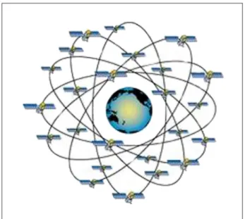
The Global Positioning System (GPS) is a collection of satellites owned by the U.S. government that provides highly accurate, worldwide positioning and navigation information, 24 hours a day. It is made up of 24 NAVSTAR GPS satellites (Figure 1), which orbit 12000 miles (about 20000 km) above the Earth, constantly transmitting the precise time and their position in space. GPS receivers, anywhere on (or near) the Earth's surface, listen on the information received from three to twelve satellites and, from that, determine the precise location and time of the receiver, as well as how fast and in what direction it is moving [1].
The GPS has found its way into the consumer market. GPS systems are available in cars, watches, cell phones etc. There is much recent research on integrating all CMOS transceiver systems on chip [2-7]. A single-chip GPS receiver was designed using 0.18 m CMOS. The receiver works in the GPS L-1 band at 1575.42 MHz, which carries the C/A code.
ARCHITECTURE AND SPECIFICATIONS A low-IF architecture with 4 MHz IF was chosen. The low-IF frequency guarantees a low energy at the image frequency and the feasibility of an integrated IF lter at a relatively low power consumption. With IF of 4 MHz, since the image-frequency of the C/A code lies in the P-code band, no other strong signals are present in this band and only 15 dB image rejection is needed to limit the noise gure degradation, due to
*. Corresponding Author, Department of Engineering, Alzahra University, Vanak, Tehran, I.R. Iran.
1. KavoshCom Asia Company, No. 291, Motahari Ave., Tehran, I.R. Iran.
Figure 1. GPS satellites constellation.
image noise, to less than 0.15 dB [2]. Direct conversion and low-IF architecture are the most popular wireless receiver architectures today. Direct conversion avoids the problem of image frequency, but issues associated with low-frequency noise, DC oset and LO-leakage, makes its implementation extremely dicult. Fre-quency planning of the proposed receiver is chosen to keep reference clock harmonics and any wireless transmissions far away from the signal and image bands.
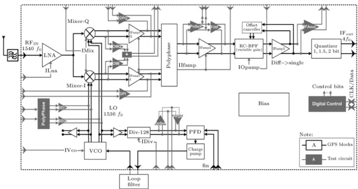
The front-end of the receiver is a quadrature low-IF receiver, consisting of a Low Noise Amplier (LNA), image rejection, using IQ mixers and a passive polyphase lter. The IF path includes a programmable gain active band-pass lter, two IF ampliers and a quantizer. The quadrature dierential LO signals, switching two double-balanced mixers, are produced
Figure 2. GPS receiver block diagram with the test circuits and test pins.
by a synthesizer block. The receiver uses only a few external passive components for the LNA input matching circuit and PLL loop lter. The non-grey blocks in Figure 2 show the receiver architecture.
In analog circuit design, especially RF design, exact circuit models, consisting of all parasitic, are critical. Although the circuit models become more precise with time, RF/analog circuits must be taped out three, four or more times to achieve the nal spec. A programmable GPS receiver has been designed with eight programming modes, one for normal operation and the others for testing the receiver blocks. The re-ceiver modes were designed to test the circuit blocks in the closest possible condition to their actual operation, instead of resorting to separate test structures that consume large Si areas (due to inductors). Therefore, after the rst tape-out, all of the circuit problems could be recognized; hence, a minimum number of needed tape outs.
RECEIVER PATH RF Section
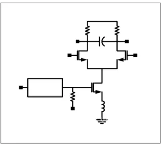
The GPS input signal is applied to a common source conguration LNA, with inductive degeneration pro-viding a high voltage gain, a low noise gure and sucient linearity. A single-ended LNA has been pre-ferred to a balanced one to reduce power consumption and silicon area. Substrate noise has been eliminated, using deep N-Well. The cascade conguration increases LNA gain, reduces the eect of Miller capacitance and
increases LNA reverse isolation. In the LNA circuit (Figure 3), R1 is used for dc biasing and C1 for
by-passing. Lg controls gain and noise matching, C2
aects input matching and the noise gure, LL and
CL are tuning circuits and Ls aects gain, linearity
and noise matching. The LNA features a 2.5 dB noise gure at 1.57 GHz, an 18 dB voltage gain, a 250 MHz bandwidth and lower than -12 dB S11 over the LNA passband. The LNA draws 2.5 mA from a 1.8 V supply yielding 4.5 mW power consumption.
The 1.57 GHz RF signal is quadrature down-converted by the I-Q single balanced mixers (Figure 4), which are ac coupled to the LNA. Single-balanced
Figure 4. A single-balanced mixer.
mixers have lower input noise than double-balanced mixers for the same power consumption. The problem of a single-balanced mixer is the leakage of LO fre-quency to the output. Since the LO frefre-quency is much higher than the IF, the output LO frequency would be eliminated completely by the limited bandwidth IF path. The load is a simple resistor. The current consumption is 1.26 mA for each mixer, the mixer gain is 16 dB and the LO rejection is -32 dB.
IF Section
The down-converted signal is amplied using an IF amplier. A second-order integrated passive polyphase lter (Figure 5) has been used to recombine I and Q signal paths after rejecting the image noise. A combination of I and Q signal paths in a single real path decreases power consumption and the chip area. The polyphase lter is an RC structure with inputs and outputs symmetrically disposed. A polyphase RC passive lter has zero power consumption, high image rejection, low sensitivity to mismatching in components and high linearity. The average image noise rejection of the polyphase lter is 20 dB [8].
The IF-chain performs ltering and further am-plication. An active RC lter is the best choice for its high linearity, high dynamic range and variable gain.
Figure 5. A second-order polyphase lter.
Although the lter noise is high, it has no eect on the receiver input noise, due to the high gain of the LNA, the mixer and the IF amplier chain. A cascade of a bandpass and a low-pass lter is used to implement a fourth-order transfer function [3]. Programmable capacitor and resistor banks control the gain of the two lter stages without aecting the frequency response and bandwidth. The designed lter is centered at 40,
where f0 = 1:023 MHz and has a 5 MHz bandwidth
to cover the input signal spectrum over a wide range of temperature and process changes. The lter gain changes from -3 dB to 52 dB and the ltered signal is amplied by an IF amplier. The maximum gain of the IF-chain is 86 dB, with a 55 dB gain range. With 34 dB front-end gain, a 120 dB total on-chip gain is achieved. The quantizer quantizes the unsampled signal to a selectable level of 1, 1.5 or 2b. The IF strip draws 5.54 mA from a 1.8 V voltage supply.
SYNTHESIZER
The quadrature LO signals are generated for the receiver with a fully-integrated second order type-II Phase Locked Loop (PLL) frequency synthesizer. It has a low phase noise fully-integrated quadrature LC VCO, which uses 4 nH square inductors with a Q of 6 and MOS varactors (Figure 6). The VCO frequency tuning range is about 400 MHz (considering process variation, a temperature range of between -40 to 125 degrees and 10% variation on the L and C values). The minimum signal output amplitude of the VCO is about 0.2 Vp-p, because the mixer conversion gain drops at the smaller amplitude. The VCO output is divided by 128 and compared with the reference frequency. Each divide-by-2 block consists of two master slave ipops implemented by CML logic with resistive loads. Each ip-op is optimum for speed and power. The charge pump sends 0.3 mA current pulses to the o-chip loop lter and the resulting voltage controls the VCO frequency. Table 1 shows the synthesizer specications.
Table 1. The synthesizer specications. Synthesizer
PLL spurs -60 dBc
Reference frequency 12.276 MHz Phase noise @ 1 MHz -105 dBc/Hz
Lock time < 10 s
RMS phase error 6 degree Current consumption 6.5 mA
Figure 7. Staggered wafers method.
DESIGN FOR TESTABILITY
Trouble shooting methods are staggered wafers with ex-tra devices, test structures and a design for testability. The staggered wafers need some resistors/capacitors and device arrays placed on the whole chip, for con-necting to the circuit when necessary. One starts with about 20 wafers and some wafers are put on hold in
progress of the fabrication.
This method uses a standard test array and needs access to the circuit connections (Figure 7). The test structure method uses on-chip test structures and the main circuit blocks are placed twice on the chip; one for full function and small pieces for testing. It needs a large number of pins to access these blocks and the masks cannot be used for production.
In the design for a testability method, some input and output drivers are considered to drive the input port and test the output port signal of the main circuit blocks. Several test modes are dened to test each block separately. A large number of controlling signals, or a shift register with input programming signals and logic circuits, to produce the controlling signals, are needed.
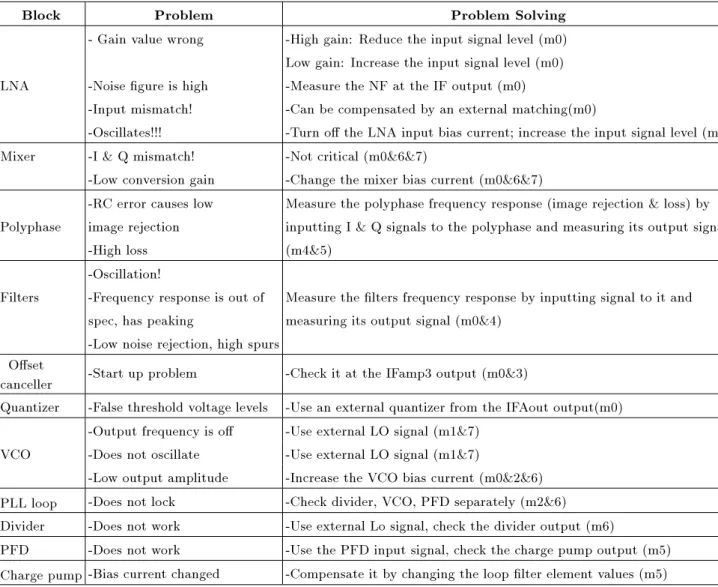
Each circuit block could have a defect after fabrication, due to insucient modeling. Some test circuits are added for detecting the defective block and testing the other receiver blocks in the test structures method. Table 2 shows all probable problems and their problem solving approaches for the receiver blocks.
The test circuits and internal test pins are added to the receiver, as shown in the grey colored sections of Figure 1. The additional circuit only adds 4% to the Si area. A critical item to the success of this approach is shown in Figure 8. By activating the buer circuits, RF blocks can be tested in their original form and, by making them high impedance, a normal operational mode is possible without disturbance. The additional test structures, based on Figure 7, are as follows: 1. Input drivers: DPI & DPQ (4 MHz quadrature
inputs), FiltF (4 MHz lter inputs), PFDF (12 MHz PFD inputs),
2. Output drivers: OMI & OMQ (4 MHz mixer
Table 2. All of the GPS receiver probable problems and the problem solving (note: MX MODE X).
Block Problem Problem Solving
- Gain value wrong -High gain: Reduce the input signal level (m0) Low gain: Increase the input signal level (m0) LNA -Noise gure is high -Measure the NF at the IF output (m0)
-Input mismatch! -Can be compensated by an external matching(m0)
-Oscillates!!! -Turn o the LNA input bias current; increase the input signal level (m0) Mixer -I & Q mismatch! -Not critical (m0&6&7)
-Low conversion gain -Change the mixer bias current (m0&6&7)
-RC error causes low Measure the polyphase frequency response (image rejection & loss) by Polyphase image rejection inputting I & Q signals to the polyphase and measuring its output signal
-High loss (m4&5)
-Oscillation!
Filters -Frequency response is out of Measure the lters frequency response by inputting signal to it and spec, has peaking measuring its output signal (m0&4)
-Low noise rejection, high spurs Oset
canceller -Start up problem -Check it at the IFamp3 output (m0&3)
Quantizer -False threshold voltage levels -Use an external quantizer from the IFAout output(m0) -Output frequency is o -Use external LO signal (m1&7)
VCO -Does not oscillate -Use external LO signal (m1&7)
-Low output amplitude -Increase the VCO bias current (m0&2&6) PLL loop -Does not lock -Check divider, VCO, PFD separately (m2&6) Divider -Does not work -Use external Lo signal, check the divider output (m6)
PFD -Does not work -Use the PFD input signal, check the charge pump output (m5) Charge pump -Bias current changed -Compensate it by changing the loop lter element values (m5)
outputs), PoSen (4 MHz polyphase outputs) and DoSen (12 MHz divided-by-128 outputs);
3. LO drivers: BEI & BEQ (1.57 GHz Mixer LOs). The test structures require many pins. A serial input digital block is used to minimize additional pins. Eight working modes were designed for the receiver, one for normal operating and the others for checking all of the circuit blocks (Table 3). 20 additional pins are considered for all of the testing modes; 6 input bias current test pins to control the main circuit blocks (bias currents for the LNA, Mixer, IF Amps, Filter OpAmps, VCO and dividers are programmable), 2 External input LO pins, 4 input pins for I & Q IF signals, 2 output pins to check the mixers output, 2 input/output pins to check polyphase outputs or IF input signal for the lter, 2 output pins to check IFAmp3 output and 2 input/output pins to check the divider output or 12 MHz input signal for PFD. After removing all of the circuit defects, the additional testing pins can be
used as VCC and GND inputs to reduce their parasitic
elements values.
All receiver blocks were tested separately after the rst tape-out, using the dened working modes. All the blocks specs, except the VCO, met the simulation results. The VCO oscillated at 1.9 GHz. The RF-IF path and the divider block were tested with external LO frequency, using m1 and m7 modes. The problem was solved in the next tape-out.
MEASUREMENT RESULTS
The receiver is fabricated in a standard 0.18 m CMOS deep N-Well process. The chip specications are summarized in Table 4.
The IF lter frequency response and variable gain range are shown in Figure 9. The pass-band ripple is less than 0.5 dB. Figure 10 shows the 1,2-bit quantizer output. The GPS receiver has been housed in a standard 48-pin TQFP package that allowed multiple
Table 3. Eight working modes for the GPS receiver (M0-7). Normal Ext.
VCO
VCO Test
IF Test
RC Filter
PFD Poly
Mixer VCO Test
Mixer Ext. VCO
DPIQ O O X On X On O O
OMIQ O O X O X O On On
IFampA On On X O X O O O
PoSen O O X O O On X X
FiltF O O X O On O X X
IAampB On On X On O O X X
IFAout On On X On On X X X
VCO O On O On On On O On
DIV O O O O On On O O
DoSen On O O X X On O X
PFDF O On On X X O On X
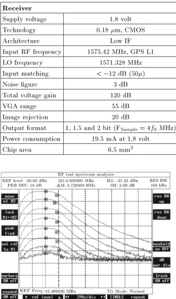
Table 4. The GPS receiver specications. Receiver
Supply voltage 1.8 volt
Technology 0.18 m, CMOS
Architecture Low IF
Input RF frequency 1575.42 MHz, GPS L1
LO frequency 1571.328 MHz
Input matching < 12 dB (50)
Noise gure 3 dB
Total voltage gain 120 dB
VGA range 55 dB
Image rejection 20 dB
Output format 1, 1.5 and 2 bit (FSample= 4f0 MHz) Power consumption 19.5 mA at 1.8 volt
Chip area 6.5 mm2
Figure 9. IF lter frequency response and variable gain range.
Figure 10. a) 1-bit quantizer output; and b) 2-bit quantizer output.
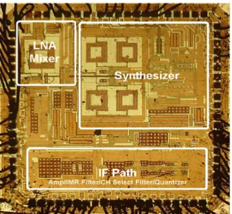
ground and test pins. A micrograph of the 6.5 mm2IC
is shown in Figure 11.
CONCLUSION
A low-IF GPS radio was implemented in a 0.18 m CMOS process with a 19.5 mA power consumption in 6.5 mm2. A serial input digital control, with an
Figure 11. A micrograph of the GPS receiver.
additional testing structure, is used in the actual RF circuits, in case of problems, minimizing the number of Si runs.
REFERENCES
1. Rabaeijs, A. et al. \GPS receiver prototype for integra-tion into system-on-chip", IEEE Trans. on Customer
Electronics, 49, pp 48-58 (Feb. 2003).
2. Behbahani, F. et al. \A 27-mW GPS radio in 0.35-um CMOS", IEEE Int. Solid-State Circuits Conf. Dig. Tech. Papers, pp 398-399 (Feb. 2002).
3. Motagna, G. et al. \A 35-mW 3.6-mm2 fully integrated 0.18-m CMOS GPS radio", IEEE J. Solid-State Circuits, 38, pp 1163-1171 (July 2003).
4. Kadoyama, T. et al. \A complete single-chip GPS receiver with 1.6-V 24-mW radio in 0.18-m CMOS", IEEE J. Solid-State Circuits, 39, pp 562-568 (April 2004).
5. Vancorenland, P. et al. \A fully integrated GPS receiver front-end with 40-mW power consumption", in IEEE Int. Solid-State Circuits Conf. Dig. Tech. Papers, pp 396-397 (Feb. 2002).
6. Steyaert, M. et al. \A fully integrated GPS receiver front-end with 40-mW power consumption", IEEE Int. Solid-State Circuits Conf. Dig. Tech. Papers, pp 396-397 (Feb. 2002).
7. Shaeer, D.K. et al. \A 115-mW, 0.5m CMOS GPS receiver with wide dynamic-range active lters", IEEE J. Solid-State Circuits, 33, pp 2219-2231 (Dec. 1998). 8. Behbahani, F. et al. \CMOS mixers and polyphase lters for large image rejection", IEEE J. Solid-State Circuits, 36, pp 873-887 (June 2001).