Area–time efficient hardware architecture for
factoring integers with the elliptic curve method
Jan Pelzl, Martin Sˇimka, Thorsten Kleinjung, Jens Franke, Christine Priplata, Colin Stahlke, Milosˇ Drutarovsky´, Viktor Fischer and Christof Paar
Abstract: Since the introduction of public key cryptography, the problem of factoring large composites has been of increased interest. The security of the most popular asymmetric cryptographic scheme RSA depends on the hardness of factoring large numbers. The best known method for factoring large integers is the general number field sieve (GNFS). One important step within the GNFS is the factorization of mid-size numbers for smoothness testing, an efficient algorithm for which is the elliptic curve method (ECM). Since smoothness testing is also suitable for parallelization, the implementation of ECM in hardware is promising. We show that massive parallel and cost-efficient ECM hardware engines can improve the area–time product of the RSA moduli factorization via the GNFS considerably. The computation of ECM is a classic example of an algorithm that can be significantly accelerated through special-purpose hardware. We thoroughly analyse the prerequisites for an area–time efficient hardware architecture for ECM. We present an implementation of ECM to factor numbers up to 200 bits, which is also scalable to other bit lengths. ECM is realized as a software–hardware co-design on a field-programmable gate array (FPGA) and an embedded microcontroller (system-on-chip). Furthermore, we provide estimates for state-of-the-art CMOS implementation of the design and for the application of massive parallel ECM engines to the GNFS. This appears to be the first publication of a realized hardware implementation of ECM, and the first description of GNFS acceleration through hardware-based ECM.
1 Introduction
Since ancient times, factoring integers has been investi-gated painstakingly by many mathematicians. With the dawn of asymmetric cryptography in the mid-1970s the problem of factoring large composites has again attracted increased mathematical interest. These days, by far the most popular asymmetric cryptosystem is RSA, which was developed by Ronald Rivest et al. in 1977 [1]. The security of the RSA cryptosystem relies on the difficulty of factoring large numbers. Hence, the development of a fast factorization method could allow cryptanalysis of RSA messages and signatures.
However, until now the problem of factorization has remained hard.
Several efficient algorithms for factoring integers have been proposed. Each algorithm is appropriate for a different situation. For instance, the elliptic curve method (ECM, see [2]) allows for efficient factoring of numbers with relatively small factors. The general number field sieve (GNFS, see [3]) is best for factoring numbers with large factors and, hence, can be used for attacking the RSA cryptosystem. In the GNFS many mid-size integers arise that have to be checked for smoothness, i.e. whether they decompose completely into small prime factors. The sieving step of the GNFS finds some of these factors. After dividing them out, we obtain a co-factor that has to be checked for smoothness. We call this co-factorization or smooth-ness testing. An appropriate choice for this task is the multiple polynomial quadratic sieve (MPQS) or the ECM.
The current world record in factoring a random RSA modulus is 200 decimals and was achieved with a complete software implementation of the GNFS in 2005 [4], using the MPQS for the factorization of the cofactors. For larger moduli it will become crucial to use special hardware for factoring. Recently, some new hardware architectures for the sieving step in the GNFS have been proposed (e.g. SHARK [5], TWIRL [6]). The efficiency of SHARK, for example (and possibly other innovative GNFS realizations) is directly related to efficient support units for smoothness testing within the architecture.
It appears that the use of the ECM rather than the MPQS is the better choice for this task, since the MPQS requires a larger silicon area and irregular operations. ªIEE 2005
IEE Proceedingsonline no. doi:10.1049/ip-ifs: Paper first received
Jan Pelzl and Christof Paar are with the Horst Go¨rtz Institute for IT Security, Ruhr University Bochum, Germany
E-mail: {pelzl, cpaar}@crypto.rub.de
Martin Sˇimka and Milosˇ Drutarovsky are with the Department of Electronics and Multimedia Communications, Technical University of Kosˇice, Park Komenske´ho 13, 04120 Kosˇice, Slovak Republic
E-mail: {Martin.Simka, Milos.Drutarovsky}@tuke.sk
Thorsten Kleinjung and Jens Franke are with the Department of Mathematics, University of Bonn, Beringstraße 1, D-53115 Bonn, Germany E-mail: {thor, franke}@math.uni-bonn.de
Christine Priplata and Colin Stahlke are with EDIZONE GmbH, Siegfried-Leopold-Straße 58, D-53225 Bonn, Germany
E-mail: {priplata, stahlke}@edizone.de
Viktor Fischer is with the Laboratoire Traitement du Signal et Instrumentation, Unite´ Mixte de Recherche CNRS 5516, Universite´ Jean Monnet, 10, rue Barrouin, 42000 Saint-Etienne, France
On the other hand, the ECM is an almost ideal algorithm for dramatically improving the area–time (AT) product through special-purpose hardware. First, it performs a very high number of operations on a very small set of input data and is thus not very I/O intensive. Second, it requires relatively little memory. Third, the operands needed for supporting the GNFS are well beyond the width of current computer buses, arithmetic units, and registers, so that special-purpose hardware can provide a much better fit. This justifies the higher development costs compared with a solution with DSPs. Lastly, it should be noted that the nature of the smoothness testing in the GNFS allows for a very high degree of parallelization. Hence, the key for efficient ECM hardware lies in fast arithmetic units. Such units for modular addition and multiplication have been studied thoroughly in the past few years, e.g. for use in cryptographic devices using elliptic curve cryptography (ECC), see e.g. [7, 8]. Therefore, we could exploit the well-developed area of ECC architectures for our ECM design.
In this work, we present an efficient hardware implementation of the ECM to factor numbers up to 200 bits, which is also scalable to other bit lengths. We provide an elaborate specification of an AT efficient ECM architecture, especially suited for hardware implementations. For proof-of-concept purposes, the ECM architecture has been realized as a software– hardware co-design on an FPGA and an embedded microcontroller (system-on-chip). Timings of the real hardware for the operations of the ECM algorithm are presented. We also provide estimates for a state-of-the-art CMOS implementation of the design and for the application of massive parallel ECM engines to the GNFS. Our design has a good scalability to larger and smaller bit lengths. In some range, both the time and the silicon area depend linearly on the bit length. Such a design perfectly fits the needs of more recent proposals for hardware architectures for the GNFS (see, e.g. [5]) and can reduce the overall costs of a GNFS device considerably.
There are many possible improvements of the original ECM. Based on these improvements, we have adapted the method to the very restrictive memory requirements of efficient hardware, thus minimizing the AT product. The parameters used in our imple-mentation are best suited to finding factors of up to 40 bits.
For the implementation, a highly efficient modular multiplication architecture described by Tenca and Koc¸ [9] is used which allows for reliable estimates for a future application-specific integrated circuit (ASIC) implemen-tation. We propose grouping1000 ECM units together on an ASIC and describe a controlling unit that syn-chronously feeds the units with programming steps, So that the ECM algorithm does not need to be stored in every single unit. In this way we keep the overall ASIC area small and still do not need much bandwidth for communication.
Section 3 introduces ECM and some optimizations relevant for our implementation. The choice of para-meters and arithmetic algorithms, the design of the ECM unit and a possible parallelization are described in Section 4. The next two sections present our FPGA implementation, some estimates for a realization as an ASIC implementation and a case study of GNFS support with ECM hardware. The last section collects results and conclusions.
2 Previous work on ECM in software and hardware
To our knowledge, ECM has never been implemented in hardware before. In the context of special-purpose hardware for the GNFS, [10] mentions that the construc-tion of special ECM hardware might be promising for supporting the GNFS. However, we are not aware of any publication dealing with ECM hardware until now. ECM is related to elliptic curve cryptosystems; hence, hardware implementations of recent elliptic curve cryptosystems using Montgomery coordinates may also be of interest. The advantage of the use of Montgomery form curves in cryptography is the inherent resistance to side channel attacks due to almost indistinguishable group operations; i.e. the elementary operations for addition and duplication of points are quite similar. A handicap of the Montgomery form is the fact that not every arbitrary curve can be transformed into Montgomery form. Hence, there is merely interest in implementing ECC based on Montgomery form curves. A parallel software implementation of the ECM on several workstations (Pentium II @ 350 MHz, Linux OS) is reported in [11]. The implementation uses fast network switches and has been programmed based on the Message-Passing Interface standard.
Two massively parallel implementations of ECM based on systolic versions of the Montgomery modular multiplication are described in [12]. The authors apply a single instruction, multiple data approach on a particular type of parallel computer. Furthermore, they achieve an efficiency improvement by applying a computational trick to reduce the weight of the scalars. A well-known free software implementation of the ECM to factor integers is available from [13] (GMP-ECM). The implementation is based on the GNU Multiple Precision Arithmetic Library (GMP). The original purpose of the project was to find a factor of 50 digits or more by ECM. Through the participa-tion of several developers, GMP-ECM is an excellent resource for a state-of-the-art ECM software implemen-tation, including many useful algorithms.
3 Elliptic curve method
The principles of the ECM are based on Pollard’s (p1) method ([14]). In the following, we describe H. W. Lenstra’s ECM (see [2]).
3.1
The algorithm
LetNbe an integer without small prime factors which is divisible by at least two different primes, one of themq. Such numbers appear after trial division and a quick prime power test.
LetE=Qbe an elliptic curve with good reduction at all prime divisors ofN(this can be checked by calculating the gcd ofNand the discriminant ofE, which very rarely yields a prime factor ofN) and a pointP2EðQÞ. Let
EðQÞ !EðFqÞ, Q7!Q be the reduction modulo q. If
the order o of P2EðFqÞ satisfies certain smoothness
conditions described below, we can discover the factor
q of N as follows. In the first phase of the ECM, we calculateQ¼kP, wherekis a product of prime powers
pe4B1with appropriately chosen smoothness bounds.
The second phase of the ECM checks for each prime
B1<p4B2whether pQreduces to the neutral element
for both phases of the ECM. Phase 2 can be done efficiently, e.g. using the Weierstraß form and projective coordinates pQ¼(xpQ : ypQ : zpQ) by testing whether gcd(zpQ, N)>1. Note that we can avoid all gcd com-putations but one at the expense of one modular multiplication per gcd by accumulating the numbers to be checked in a product moduloNand performing one final gcd.
If we are using only one single curve, the properties of the ECM are related to those of Pollard’s (p1) method. The advantage of the ECM lies in the possibility of choosing a different curve after each trial to increase the probability of finding factors ofN.
All calculations are done moduloN. If the final gcd of the product P and N satisfies 1<gcd(P, N)<N, a factor is found. The parameters B1 and B2 control
the probability of finding a divisor q. More precisely, if o factors into a product of co-prime prime powers (each4B1) and at most one additional prime between
B1andB2, the prime factorqis discovered.
The procedure will be repeated for other elliptic curves. To generate them one commences with the starting point P and constructs an elliptic curve such thatPlies on it (see Appendix 9.1).
It is possible for more than one or even all prime divisors of N to be discovered simultaneously. This happens rarely for reasonable parameter choices and can be ignored by proceeding to the next elliptic curve.
The running time of the ECM is given by
TðpÞp!1¼ e ffiffiffiffiffiffiffiffiffiffiffiffiffiffiffiffiffiffiffiffiffiffi2 logplog logp p
ð1þoð1ÞÞ
operations; thus, it mainly depends on the size of the factors to be found and not on the size of N [15]. (Remark: The operations are computed modN; hence, the running time of the operations depends onN.)
3.2
The elliptic curves
Apart from the Weierstraß form there are various other forms for the elliptic curves. We use Montgomery’s form (1) and compute in the set S¼EðZ=NZÞ=f1g only using thex- andz-coordinates.
By2z¼x3þAx2zþxz2 ð1Þ This was suggested in [16] by Montgomery. Curves of this form always have an order divisible by 4; i.e. not every curve can be transformed to the Montgomery form. In our case, the curves can be chosen in such a way that they have an order divisible by 12. Appendix 9.1 describes the construction of such curves.
The residue class ofPþQin this set can be computed from P, Q and PQ using six multiplications (2). A duplication, i.e. 2P, can be computed from P using five multiplications (3). Since we are only interested in checking whether we obtain the point at infinity for some prime divisor of N, computing in S is no restriction. In the following we will not distinguish between EðZ=NZÞ and S, and pretend to do all computations inEðZ=NZÞ. Addition: xPþQzPQ½ðxPzPÞðxQþzQÞ þ ðxPþzPÞðxQzQÞ2 ðmodNÞ zPþQxPQ½ðxPzPÞðxQþzQÞ ðxPþzPÞðxQzQÞ2 ðmodNÞ ð2Þ Duplication 4xPzP ðxPþzPÞ2 ðxPzPÞ2 ðmodNÞ x2P ðxPþzPÞ2ðxPzPÞ2 ðmodNÞ z2P4xPzP½ðxPzPÞ2 þ4xPzPðAþ2Þ=4 ðmodNÞ ð3Þ
3.3
The first phase
If the triple (P,nP, (n þ1)P) is given we can compute (P, 2nP, (2nþ1)P) or (P, (2nþ1)P, (2nþ2)P) by one addition and one duplication in Montgomery’s form. Thus Q¼kP can be calculated using [log2k]
additions and duplications according to Algorithm 2,
amounting to 11[log2k] multiplications. In the case
zP¼1 we can reduce this to 10[log2k] multiplications.
By handling each prime factor of k separately and using optimal addition chains the number of multi-plications can be decreased to roughly 9.3[log2k] [16].
The addition chains can be precalculated.
3.4
The second phase
The standard way to calculate the points pQ for all primes B1<p4B2 is to precompute a (small) table of
multiples kQ where k runs through the differences of consecutive primes in the interval ]B1, B2]. Then, p0Q
is computed with p0 being the smallest prime in
that interval and the corresponding table entries are added successively to obtain pQ for the next prime p. Algorithm 1: ECM
Phase 1:
1. Choose arbitrary curveE=Qand random pointP2EðQÞ 6¼ O. 2. Choose smoothness boundsB1;B22Nand compute
k¼ Y pi2P;piB1 pepi i ; epi¼maxfq2N:p q i B2g: 3. ComputeQ¼kP¼(xQ,yQ,zQ) andd¼gcd(zQ,n). Phase 2: 1. SetP:¼1.
2. For each primepwith B1<p4B2computepQ¼(xpQ:ypQ:
zpQ) andP¼PzpQ.
3. Computed¼gcd(P,N).
4. A non-trivial factordis found, if 1<d<N. Else: restart from Step 1 in Phase 1.
Algorithm 2: Exponentiation for curves in Mon-tgomery form
INPUT: Integerg>1 withg¼ ðgtgt1. . .g1g0Þ2and a pointPon the curveEM:By2 ¼x3 þAx2 þx. OUTPUT: ProductQ¼gP. 1.Pn¼P Pnþ1¼2P 2.fori¼t1to1do: (a)ifgi¼1,then Pn¼PnþPnþ1 Pnþ1¼2Pnþ1 (b)else Pnþ1¼PnþPnþ1 Pn¼2Pn 3.ifg0¼1,thenQ¼Pn þ Pnþ1 4.elseQ¼2Pn. 5.returnQ
Two major improvements have been proposed for the ECM [17, 16]. Using Montgomery’s form, the procedure is difficult to implement but can be improved as follows. The following lemma allows us to reduce the complexity by repeatedly multiplying a difference of two products instead of computing complex point operations in each step of Phase 2:
Lemma 1 Let q ¼a þb, with a and b co-prime. Furthermore, let qQ¼AþB, with A¼aQ and B¼bQ, then zqQ ¼0 mod t for gcd(zQ, N)¼1 if and
only if
xAzBzAxB0 modt Proof
(1) Montgomery’s point addition formula yields
tjzqQ,tjxAB½xAzBzAxB2
(tjðxAzBzAxBÞ
(2) if zqQ0 mod t, qQ is the identity point on the elliptic curve overFt. Hence,A¼ B; i.e. AandBare
zero or
xA=zAxB=zBmodt
A¼B¼0 yields Q¼0, thus t|zQ, which is a contradiction to the assumption of gcd(zQ, n)¼1. Then we have
xA=zAxB=zB modt and
xAzBzAxB mod t respectively
The improved standard continuation uses a para-meter 2<D<B1. First, a table T of multiples kQ of
Q for all 14k<D/2, gcd(k, D)¼1 is calculated. Each primeB1<p4B2can be written asmD±kwith
kQ 2 T. Now, with Lemma 1 gcd(zpQ, N)>1 if and only if gcd(xmDQzkQxkQzmDQ, N)>1. Thus, we calculate the sequencemDQ (which can easily be done in Montgomery’s form) and accumulate the product of allxmDQzkQxkQzmDQfor whichmDkormDþkis prime.
The memory requirements for the improved standard continuation are j(D)/2 points for the table T and the points DQ, (m1)DQ, mDQ for computing the sequence, altogether j(D)þ6 numbers. The com-putational costs consist of the generation of T and the calculation of mDQ, which amounts to at most
D/4þB2/Dþ7 elliptic curve operations (mostly
additions) and at most 3(p(B2)p(B1)) modular
multi-plications,p(x) being the number of primes up tox. The last term can be lowered ifDcontains many small prime factors since this will increase the number of pairs (m,k) for which both mDk and mDþk are prime. Neglecting space considerations, a good choice for
Dis a number around ffiffiffiffiffiffiB2
p
, which is divisible by many small primes.
4 Methodology
We will now discuss the parameterization of ECM, optimized for our purposes. Finally, the design of the ECM unit is described.
4.1
Parameterization of the ECM algorithm
Our implementation focuses on the factorization of numbers up to 200 bits with factors of up to 40 bits.
Thus, ‘good’ parameters for B1, B2, and Dhave to be
found, yielding a high probability of success and a relatively small running time and area consumption. With the running time depending on the size of the (unknown) factors to be found, optimal parameters cannot be known beforehand. Hence, good parameters can be found by experiments with different prime bounds.
On the basis of deduction from software experiments, we chooseB1¼960 andB2¼57 000 as prime bounds.
The value ofkhas 1375 bits; hence, assuming the binary method (Algorithm 2), 1374 point additions and 1374 point duplications for the execution of Phase 1 are required. Due to the use of Montgomery coordinates, the coordinatezPof the starting pointPcan be set to 1; thus, addition takes only five multiplications instead of six. The improved Phase 1 (with optimal addition chains) has to use the general case, wherezP6¼1. For the sake of simplicity and a preferably simple control logic, we choose the binary method for the time being. For the chosen parameters, the computational complexity of Phase 1 is 13 740 modular multiplications and squarings. (In this contribution, squarings and multi-plications are considered to have an identical complexity since the hardware will compute a squaring with the multiplication circuit. With optimized addition chains this number can be reduced to12 000 modular multipli-cations and squarings.)
According to (3), duplicating a point 2PA¼PC involves the input values xA, zA, A24 and N, where
A24¼(Aþ2)/4 is computed from the curve parameter
A[see (1)] in advance and should be stored in a fixed register. A point addition PC¼PAþPB handles the input valuesxA,zA,xB,zB,xAB, zAB andN[see (2)]. Notice that during Phase 1 the valuesN,A24,xABand
zAB do not change. Furthermore, zAB¼z1 can be
chosen to be 1. Thus, no register is required forzAB. The output valuesxC and zC can be written to certain input registers to save memory. If we assume that the ECM unit does not execute addition and duplication in parallel, at most seven registers for the values in Z=NZ are required for Phase 1. Additionally, we will require four temporary registers for intermediate values. Thus, a total of 11 registers is required for Phase 1.
For the prime bounds chosen, 5621 primesp2[B1,B2]
have to be tested in Phase 2. With the prime bounds fixed, the computational complexity depends on the size ofD. Hence, Dshould consist of small primes in order to keepj(D) as small as possible. We consider the cases
D¼6,D¼30,D¼60 andD¼210. The initial values can be computed by first computing QQ^¼DQ, then ðB1=DÞQQ^with the binary method, yielding automatically
½ðB1=DÞ 1QQ^. The total number of modular
multi-plications is determined by the number of point additions, point duplications and multiplications for the product P. Table 1 displays the computational complexity and the number of registers required additionally for Phase 2. For the numbers in the table, we assume the use of Algorithm 2 for computing the initial values; e.g. in the caseD¼30, the cost for the computation ofDQ, [(B1/D)1)DQ, and (B1/D)DQ is
as much as eight point additions and eight point duplications. For the same D, the computation of the table involves five point additions and two point duplications, yielding to a total of 13 590 modular multiplications. (Remark: for the caseD¼210, we start withB1¼1050 in order to ensure thatDand B1share
For Phase 2 we choose D¼30 to obtain a minimal AT product of the design. Sincej(D)¼8 is small, only eight additional registers are required to store all coordinates in a table. Unlike in Phase 1, we have to consider the general case for point addition where
zAB6¼1. Hence, an additional register for this quantity is needed. For the productPof allxAzB zAxB, one more register is necessary. The temporary registers from Phase 1 suffice to store the intermediate results
xAzB, zAxB and xAzBzAxB. Hence, 10 additional registers for Phase 2 yield a total of 21 required registers for both phases. The computational complexity of Phase 2 is 1881 point additions and 10 point duplications. Together with the 13 590 modular multiplications for computing the product P, 24 926 modular multiplications and squarings are required.
For a high probability of success (>80%) for the parameters given, software experiments suggest running the ECM on20 different curves.
4.2
Design of the ECM hardware
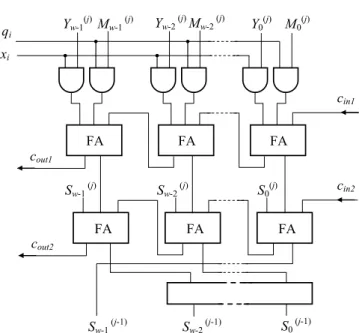
The ECM unit consists mainly of three parts: the arithmetic logic unit (ALU), the memory part (register) and an internal control logic (seeFig. 1). Each unit has a very low communication overhead since all results are stored inside the unit during computation. Before the actual computation starts, all required initial values (xP, N, A24) are assigned to memory cells of the unit.
This is the only input. The only output is the above-mentioned productP. The numberP is read from the unit’s memory only at the very end of the computation. The computation of gcd(P, N) is performed outside of the unit, namely by the central control logic. The commands for the ECM units are generated and timed by the central control logic outside. Commands are generated and timed by a central control logic outside the ECM unit(s).
4.2.1 Central control logic
The central control logic is connected to each ECM unit via a control bus (ctrl). It coordinates the data exchange with the unit before and after computation and starts each computation in the unit by a special set of commands. The commands contain an instruction for the next computation to be performed (i.e. add, subtract, multiply, square), includ-ing the input and output registers to be used (R1–R21). The start of an operation is invoked by setting thestartbit to ‘1’.
The control bus has to offer the possibility to specify which input register(s) and which output register are active. Only certain combinations of input and output registers occur, offering the possibility to reduce the complexity of the logic and the width of the control bus by compressing the necessary information. For simpli-city and clarity, we skip the further optimization of the commands. Instead, we use a clearly understandable structure for the commands. A command consists of 16 bits which are assigned as follows (LSB is left):
start operation input 1 input 2 output
X XX XXXX XXXX XXXXX
If several ECM units work in parallel, only one central control logic is needed. All commands are sent in parallel to all units. Only in the beginning and in the end do a unit’s memory cells have to be written and read out separately. Once the computations in all units are finished, an LSB of the central status register is set to ‘0’ to indicate the units’ availability for further commands.
4.2.2 Internal control logic
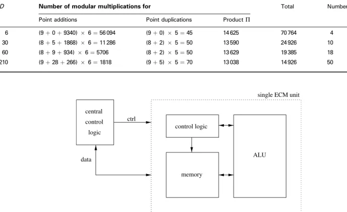
Each unit possesses an internal control logic in order to coordinate the dataTable 1: Computational complexity and memory requirements for phase 2 depending onD
D Number of modular multiplications for Total Number of registers Point additions Point duplications ProductP
6 (9þ0þ9340) 6¼56 094 (9þ0) 5¼45 14 625 70 764 4 30 (8þ5þ1868) 6¼11 286 (8þ2) 5¼50 13 590 24 926 10 60 (8þ9þ934) 6¼5706 (8þ2) 5¼50 13 629 19 385 18 210 (9þ28þ266) 6¼1818 (9þ5) 5¼70 13 038 14 926 50 control logic ctrl data control central logic
single ECM unit
memory
ALU
input and output from and to the registers, respectively. Once a command with the corresponding start bit is set, the computation inside the unit is started. Once the computation is finished, a bit is set to ‘1’ to indicate the unit’s availability for further commands. The modular arithmetic is coordinated inside the ALU and data transfer is organized by the internal control logic.
4.2.3 Memory
The addresses specified above refer to relative addresses inside each unit since we want to address the same register in multiple units in parallel. For reading from or writing to a single register in a specific unit, the unit needs to be addressed separately. In combination with a unique address for each unit, a register has a unique hardware address and can be addressed from outside the unit. This is imperative since the central control logic writes data to these registers before Phase 1 starts and it reads data from one of the registers after Phase 2 has been finished. Each register can contain n bits and is organized in e¼dnþ1/we words of sizew(seeFig. 2). Memory access is performed wordwise. Reasonable values forwarew¼4, 8, 16, 32, but these are not mandatory.4.2.4 Arithmetic logic unit
The ALU performs the arithmetic modulo 2N, i.e. modular multiplication, modular squaring, modular addition and subtraction. Possible benefits from using multiple ALUs are one ECM unit are discussed in Appendix 9.2. The objectives for the choice of implemented algorithms are mentioned in Section 4.3.4.3
Choice of the arithmetic algorithms
The main purpose of the design is to synthesize an AT efficient implementation of the ECM. Hence, all algo-rithms are chosen to allow for low area and relatively high speed. Low area consumption can be achieved by structures which allow for a certain degree of serial-ization and hence do not require much memory. For ECM, we have chosen a set of algorithms which seem to be very well suited to our purpose. In the following, we briefly describe the algorithms for modular addition, subtraction, and multiplication to be implemented for the ALU. Squaring is done with the multiplication circuit since a separate hardware circuit for squaring would increase the overall AT product. Similarly, subtraction can be computed using a slightly changed adder circuit.
4.3.1 Computing with Montgomery residues
It is well known that Montgomery multiplication [18]is an efficient method for modular multiplication. Montgomery’s algorithm replaces divisions by simple shift operations and thus is very efficient in hardware and software. The method is based on a representation of the residue class modulo the modulus N. The correspondingN-residue of an integerx is defined as
x0¼xrmodN
wherer¼2nwith 2n1<N<2nsuch that gcd(r,N)¼1 (which is always true for N odd). Since it is costly to switch always between integers and theirN-residue and vice versa, we will perform all computations in the residue class.
4.3.2 Modular multiplication
An efficient Montgom-ery multiplier, highly suitable for our design, is described in [9]. The multiplier architecture presented allows for wordwise multiplication and is scalable regarding operand size word size and pipelining depth. The internal word additions are performed by simple adders. Fig. 3 shows the architectures of one stage. Whereas in [9] a structure with carry-save adders and redundant representation of operands has been imple-mented, we have chosen a configuration with carry-propagate adders and non-redundant representation that makes a more effective implementation possible,FA FA FA FA FA FA Yw-1(j) Mw-1(j) Yw-2(j)Mw-2(j) Y0(j) M0(j) Sw-1 (j) Sw-2(j) S0(j) qi xi Sw-1 (j-1) Sw-2(j-1) S0 (j-1) cin1 cin2 cout1 cout2
Fig. 3 Multiplier stage with carry-propagate adders and
non-redundant representation
P1
2 1 0 w bits w bits w bits w bits e 2 1 0 w bits w bits w bits w bits e 21 registersP21
especially when the target platform supports fast carry chain logic. A detailed analysis and comparison of both structures can be found in [19].
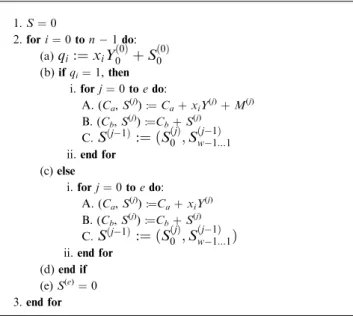
The hardware depicted performs a slightly modified multiple word radix-2 Montgomery multiplication (Algorithm 3). Instead of more expensive wordwise
addition in Step (a) we have used only bit operations. In Algorithm 3, word and bit vectors are represented as
N¼ ð0,Nðe1Þ,. . .,Nð1Þ,Nð0ÞÞ Y¼ ð0,Yðe1Þ,. . .,Yð1Þ,Yð0ÞÞ S¼ ð0,Sðe1Þ,. . .,Sð1Þ;Sð0ÞÞ X¼ ðxn1,. . .,x1;x0Þ
where words are marked with superscripts and bits are marked with subscripts.
The final reduction step of the originally proposed Montgomery multiplication can be omitted when the following condition is fulfilled:
4M<2n
With bounded input valuesX,Y<2M, the output value is also bounded (S<2M).
According to [9], the number of clock cycles per multiplication is given by (4):
Tmul¼
n
p ðeþ1Þ þ2p ð4Þ
A minimal AT product of the sole multiplier can be achieved with a word width of 8 bits and a pipelining depth of 1 (w¼8, p¼1, see [9]). However, for our ECM architecture, the AT product does not depend only on the AT product of the multiplier. In fact, the multiplier takes only a comparatively small part of the overall area. On the other hand, the overall speed relies primarily on the speed of the multiplier. Thus, we choose a pipelining depth of p¼2 for word width
w¼32 bits in order to achieve a higher speed.
4.3.3 Modular addition and subtraction
Addition and subtraction is implemented as one circuit. As with the multiplication circuit, the operations are done wordwise and the word size and number of words can be chosen arbitrary. Since the same memory is used for input and output operands, we choose the same word size as for the multiplier. The subtraction relies on the same hardware, except that one input bit has to be changed (sub¼1) in order to compute a subtraction rather than an addition (see Fig. 4, FA denotes a full adder). All operations are done modulo 2N.The actual computation is done in a wordwise manner using a word size ofw¼32. Algorithms 4 and 5 show
the elementary steps of a modular addition and subtraction, respectively.
If xþy2N, a reduction can be applied by simple subtraction of 2N. Hence, Algorithm 4 is used for the modular addition. z contains the result and T is a (temporary) register. A comparison z<2N takes the same amount of time as a subtraction T¼z2N. Thus, we compute the subtraction in all cases and decide Algorithm 3: Multiple word radix-2 Montgomery
multiplication [9] 1.S¼0 2.fori¼0ton1do: (a)qi:¼xiYð00ÞþS ð0Þ 0 (b)ifqi¼1,then i.forj¼0toedo: A. (Ca,S(j)): ¼CaþxiY(j)þM(j) B. (Cb,S(j)):¼CbþS(j) C.Sðj1Þ:¼ ðSðjÞ 0 ;S ðj1Þ w1:::1
ii.end for (c)else i.forj¼0toedo: A. (Ca,S(j)):¼CaþxiY (j) B. (Cb,S(j)): ¼CbþS(j) C.Sðj1Þ:¼ ðSðjÞ0 ;Sðjw11Þ:::1Þ
ii.end for (d)end if (e)S(e)
¼0 3.end for
Fig. 4 Addition and subtraction circuit
Algorithm 4: Modular addition
INPUT: Two integersx,y<2N
OUTPUT: Sumz¼xþymod 2N
1.z¼xþy
2.T¼z2N
3.ifT0thenz¼T
4.returnz
Algorithm 5: Modular subtraction
INPUT: Two integersx,y<2N
OUTPUT: Differencez¼xymod 2N
1.T¼z¼xy
2.ifz<0thenz¼Tþ2N
by the sign of the values which one to take as the result (zorT). IfTis the correct result, the content ofThas to be copied to the registerz.
For a modular addition, we need at most
Tadd¼3 ðeþ1Þ ð5Þ
clock cycles, where e is the number of words (for implemented non-redundant form of operands
e¼dnþ1/we). On average, we would have to reduce only every second time. However, since the control of Phase 1 and Phase 2 is parallelized for many units, we have to assume the worst case running time, which is given by (5).
The subtraction xy can be accomplished by the addition of x with the bitwise complement of y and 1. The addition of 1 is simply achieved by setting the first carry bit to one (cin¼1) (Step 1). Since the result can be negative, a final verification is required. If necessary, the modulus has to be added. Algorithm 5 describes the modular subtraction.
In Step 1, both memory cellszandTobtain the same value, which can be performed in hardware in parallel at the same time without any additional overhead. After the computation of the difference, one can check for the correctness of the result.
Hence, subtraction can be performed more efficiently than addition and requires in the worst case
Tsub¼2 ðeþ1Þ ð6Þ
clock cycles.
4.4
Parallel ECM
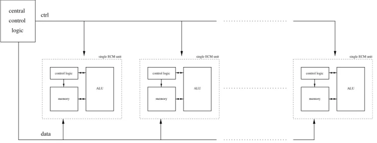
The ECM can be perfectly parallelized by using different curves in parallel since the computations of each unit are completely independent. For the control of more than one ECM unit, it is essential to know that both phases, Phase 1 and Phase 2, are controlled completely identically, independent of the composite to be factored. Fig. 5 shows the control of several ECM units in parallel.
Solely the curve parameter and possibly the modulus of the units, and hence the coordinates of the initial point, differ. Thus, all units have to be initialized differently, which is done by simply writing the values into the corresponding memory locations sequentially. During the execution of both phases, exactly the same commands can be sent to all units in parallel. Since the
running time of multiplication/squaring is constant (does not rely on input values) and for addition/ subtraction differs at most in 2(eþ1) clock cycles, all units can execute the same command at exactly the same time. After Phase 2, the results are read from the units one after another. The required time for this data I/O is negligible for one ECM unit since the computation time of both phases dominates. For several units in parallel, the computation time does not change, but the time for data I/O scales linearly with the number of units. Hence, not too many units should be controlled by one single logic. For massively parallel ECM in hardware, the ECM units can be segmented into clusters, each with its own control unit.
5 Implementation
This section presents the actual hardware implementa-tion done on a system-on-chip (FPGA and embedded microprocessor). This first hardware implementation of the ECM is designed as a proof of concept. Remark, that all timings are obtained by using real hardware, not only simulation.
5.1
Hardware platform
The ECM implementation is realized as a hybrid design. It consists of an ECM unit implemented on an FPGA (Xilinx Virtex2000E-6) and a control logic imple-mented in software on an embedded microcontroller (ARM7TDMI, 25 MHz). For more information on the hardware platform used, the interested reader is referred to [20]. The ECM unit is coded in VHDL (very high-speed integrated circuit hardware description language) and was synthesized for a Xilinx FPGA (Virtex2000E-6, [21]). For the actual VHDL implementation, memory cells have been realized with the FPGA’s internal block RAM. For simulation and synthesis FPGA Advantage tools were used; place and route was done in Xilinx ISE. The unit, as implemented, listens for commands which are written to a control register accessible by the FPGA. Required point coordinates and curve parameters are loaded into the unit before the first command is decoded. For this purpose, these memory cells are accessible from the outside by a unique address. Internal registers, which are used only as temporary registers during the computation, are not accessible from the outside.
control central
logic
control logic
single ECM unit
memory
ALU
control logic
single ECM unit
memory
ALU
control logic
single ECM unit
memory
ALU
ctrl
data
The control of the unit is done by the microcontroller present on the board which controls the data transfer from and to the units and issues the commands for all steps in Phase 1 and Phase 2. For code generation, debugging and compilation, ARM Developer Suite 1.2 was used. For details on the ARM microprocessor, see [22]. At a later stage, a soft-coded processor core (in VHDL) could be used instead of an ARM microprocessor.
The actual design was done for n¼198 bit compo-sites. The parameters for the multiplier are p¼2 and
w¼32. Scaling the design to bit lengths from 100 to 300 bits can be easily accomplished. In this case, the AT product will decrease or increase according to the size ofn2.
For a suitable implementation on a selected platform one can choose the word width w, number of words e
(length of operands), level p of pipeline stages of the multiplier and the number of ECM units. Although the implementation presented was realized on a Xilinx Virtex-E FPGA, the proposed algorithms and the design architecture can be implemented on any FPGA. Hence, a significant speed increase over state-of-the-art devices can be expected. At any rate, the platform at hand is sufficient for proof-of-concept purposes. Since the suggested clock rate of the synthesis tool was higher than the actual supported frequency of the hardware, no attempt to further accelerate the design has been made. Due to the lack of FPGA specific optimizations, the code can easily be used for different types of FPGAs.
5.2
Results
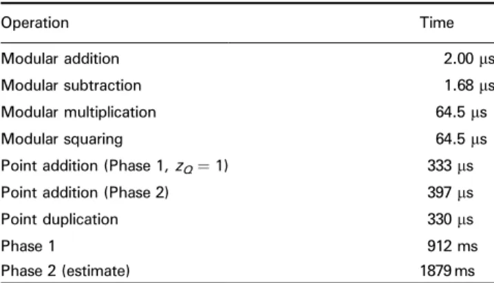
After the synthesis and place and route, the binary image was loaded onto the FPGA and clocked with a frequency of 25 MHz. Hence, the cycle length of the ALU performing the modular arithmetic is 40 ns.Table 2 shows the timings of relevant operations of the imple-mentation. The timings of both phases include the time required for data I/O. For the FPGA used, the actual design has a maximum clock frequency of 38 MHz. Due to the limits of the board’s clock generation capabilities, only 25 MHz are applied for our timing analysis.
Although a squaring is computed with the multi-plication circuit, the overhead is slightly lower, yielding a mere 0.3% faster execution. Point addition in Phase 1 is more efficient since it makes use of the fact that the
zcoordinate of the difference of points can be chosen to be 1.
We should note that the work on Phase 2 is still in progress. Though the FPGA part of Phase 2 has been
completed, the complicated control logic has still to be optimized and partially revised. Parts of Phase 2 are already running on the platform; some parts are in progress. Hence, we provide an estimate of the running time based on the running time of the timings given in Table 2. Based on experience from the complete hardware implementation of Phase 1, we believe this estimate is fairly accurate.
The ECM unit including full support for Phases 1 and 2 of the ECM with word widthw¼32 bits, number of words e¼7 and level of pipeline p¼2 has the following area requirements: 1754 LUTs, 506 flip-flops and 44 blocks RAM. Minimum clock period is 26.225 ns (maximum clock frequency: 38.132 MHz). Further improvements in data organization inside the ECM unit should yield higher performance of the whole design.
Due to the system’s latency for loading and storing values in the registers, not more than 100 ECM units (FPGA) should be controlled by one processor. With a much higher number of units the communication over-head would outweigh the computation time. However, the control logic of the data I/O has not been the focus of our optimization efforts yet, and thus we assume that slight improvements of the speed of the data I/O are still feasible. In particular, if an ASIC implementation is the target, such numbers are likely to change.
6 A case study: supporting GNFS with ECM ASICs
Building an efficient and cheap ECM hardware can influence the overall performance of the GNFS since ECM can be perfectly used for smoothness testing within the GNFS [5]. In this section, we briefly estimate the costs, space requirements and power consumption of a special ECM hardware in the form of an ASIC. In our estimate, we focus on the production cost, which we believe to be much higher than the development cost of such an ASIC. This special hardware could be produced as single ICs (such as common CPUs), ready for use in larger circuits. We choose a setting with a word width
w¼8 and assume the use of carry-save adders to allow for a higher clock rate [9].
6.1
Estimation of the running time
We can determine the running time of both phases on basis of the underlying ring arithmetic. The upper bounds for the number of clock cycles of a modular addition and a modular subtraction are given in (5) and (6), respectively. A setting with n ¼199, w¼8,
p ¼8 and e¼25 yields Tadd¼3(eþ1)¼78 and
Tsub¼2(eþ1)¼52 cycles. According to (4), the
implemented multiplier requiresTmul ¼666 cycles. For
each operation we should include Tinit¼2 cycles for
initialization of the ALU at the beginning of each computation.
For the group operations for Phase 1 we obtain
TPadd¼5Tmulþ3Taddþ3Tsubþ11Tinit
¼3742 cycles and
TPdbl¼5Tmulþ2Taddþ2Tsubþ9Tinit
¼3608 cycles
clock cycles. For phase 2, TPadd changes to
T0Padd¼4410 cycles since zAB 6¼ 1 in most cases; hence, we have to take the multiplication by zAB into account.
Table 2: Running times of the ECM implementation
(198 bits modulus),p¼2,w¼32 (Xilinx Virtex2000E-6
and ARM7TDMI, 25 MHz) Operation Time Modular addition 2.00ms Modular subtraction 1.68ms Modular multiplication 64.5ms Modular squaring 64.5ms
Point addition (Phase 1,zQ¼1) 333ms
Point addition (Phase 2) 397ms
Point duplication 330ms
Phase 1 912 ms
The total cycle count for both phases is
TPhase 1¼1374ðTPaddþTPdblÞ ¼10 098 900 and
TPhase 2¼1881T0Paddþ50TPdblþ13590Tmul¼17 553 730
clock cycles. Excluding the time for pre- and post-processing, a unit needs 27.7106 clock cycles for both phases on one curve. If we assume a frequency of 500 MHz, such a complex computation can be performed in55 ms.
6.2
Estimation of area requirements
According to [9], the multiplier with w¼8, p ¼8 requires 21 400 transistors in standard CMOS technol-ogy (assuming 4 transistors per NAND gate). (Remark: the numbers provided in [9] refer to a multiplier built with carry-save adders. Since we implemented the architecture with carry-propagate adders, given num-bers are larger (20%) than those which would be achieved with our design). We assume that the circuit for addition and subtraction can be achieved with at most 1000 transistors. For the memory, we assume (area expensive) static RAM which requires 25 200 transistors for 21 registers. For the control inside the unit we assume an additional 6000 transistors. The central control requires <2 000 000 transistors. Hence, one unit requires53 600 transistors. Assuming the CMOS technology of a standard Pentium 4 processor (0.13mm, 55 million transistors), we could fit 990 ECM units into the area of one standard processor. One ECM unit needs an area of 0.1475 mm2 and has a power dissipation of40 mW.
6.3
Application to the GNFS
Considering the architecture of [5] for a special GNFS hardware, we have to test 1.71014 cofactors up to 125 bits for smoothness. Since both the running time and the area requirement scale linearly with the bit size, we can multiply the results from the subsections above with a factor of 125/1980.628. If we distribute the computation over a whole year, we have to check 5 390 665 cofactors per second.
For a probability of success of >90%, we test 20 curves per rest; thus, we need 3 850 000 ECM units, which would yield a total chip area of 625 000 mm2 (¼4300 ICs of the size of a Pentium 4) and a power consumption of 175 kW. If we assume a cost of $5000 per 300 mm wafer, as done in [6], the ECM units would cost less than $45 000 for the whole GNFS architecture, which is negligible in the context of the overall costs.
7 Conclusions
In our current work, we present a thorough analysis of adequate algorithms for an ECM hardware architecture. The parameterization of the algorithms was done particularly to fit the needs of a hardware environment, yielding a high efficiency in terms of the AT product. Furthermore, this is the first publication showing a real hardware implementation of the ECM algorithm. The implementation is a hardware–software co-design and has been implemented on an FPGA and an ARM microcontroller for factoring integers of size up to 198 bits. We implemented a variant of the ECM which allows for a very low AT product and hence is very cost effective. Our implementation impressively shows that
due to very low area requirements and low data I/O, the ECM is predestined for use in hardware. A single unit for factoring composites of up to 198 bits requires 506 flip-flops, 1754 lookup tables and 44 Blocks RAM (<6% of logic and 27% of memory resources of the Xilinx Vertex2000E device). Regarding a possible ASIC implementation, 990 ECM units could be placed on a single Pentium 4-sized chip.
As demonstrated, the ECM can be perfectly paralle-lized, and thus an implementation at a larger scale can be used to assist the GNFS factoring algorithm by carrying out all required smoothness tests. A low-cost ASIC implementation of the ECM can decrease the overall costs of the GNFS architecture SHARK, as shown in [5]. We believe that extensive use of ECM for smoothness testing can further reduce the costs of such a GNFS machine.
As future steps, the control logic for the second phase will be finalized. Variants of Phase 2 can be examined in order to achieve the lowest possible AT product. To achieve a higher maximal clock frequency of the ECM unit, the control logic inside the unit might be optimized.
Since most of the computation time is spent on modular multiplications, an improvement of the imple-mentation of the multiplication directly affects the overall performance. Hence, alternative architectures for the multiplication can be investigated.
With the VHDL source code at hand, the next logic step is the design and simulation of a full custom ASIC containing the logic, which is currently implemented in the FPGA. For an ASIC implementation, a parallel design of many ECM units is preferable. The control can still be handled outside the ASIC by a small microcontroller, as is the case with the work at hand. Alternatively, a soft core of a small microcontroller can be adapted to the specific needs of ECM and be implemented within the ASIC. With a running ECM ASIC, exact cost estimates for the support of algorithms such as the GNFS can be obtained.
8 References
1 Rivest, R.L., Shamir, A., and Adleman, L.: ‘A method for obtaining digital signatures and public-key cryptosystems,’
Commun. ACM, 1978,21, pp. 120–126
2 Lenstra, H.W.: ‘Factoring integers with elliptic curves,’Annals of Mathematics,Vol. 126, no. 2, pp. 649–673, 1987
3 Lenstra, A.K., and Lenstra, H.W. Jr., eds.,: ‘The development of the number field sieve’. Lecture Notes in Mathematics Volume 1554 (Springer, 1993)
4 Franke, J., and Kleinjung, T.: ‘E-mail announcement’. http:// www.crypto-world.com/announcements/rsa200.txt, accessed May 2005
5 Franke, J., Kleinjung, T., Paar, C., Pelzl, J., Priplata, C., and Stahlke, C.: ‘SHARK — a realizable special hardware sieving device for factoring 1024-bit integers.’ Proc. Workshop on Cryptographic Hardware and Embedded Systems — CHES 2005, Edinburgh, August 2005,LNCS(Springer, 2005) 6 Shamir, A., and Tromer, E.: ‘Factoring large numbers with
the TWIRL device.’ Proc. Advances in Cryptology — Crypto 2003, Santa Barbara, CA, USA, August 2003, LNCS, 2729. Springer, 2003, pp. 1–26
7 Orland, G., and Paar, C.: ‘‘A ScalableGF (p) elliptic curve processor architecture for programmable hardware.’’ (Koc¸, C¸.K., Naccache, D. and Paar, C. (Eds) Proc. Workshop on Crypto-graphic Hardware and Embedded Systems—CHES 2001, Paris, France, May 2001,LNCS2162. (Springer, 2001), pp. 348–363 8 Gura, N., Chang, S., Sumit, H.G., Gupta, V., Finchelstein, D.,
Goupy, E., and Stebila, D.: ‘An end-to-end systems approach to elliptic curve cryptography,’ In Koc¸, C¸.K., and Paar, C. (Eds): Proc. Cryptographic Hardware and Embedded Systems—CHES
2002, San Francisco Bay, USA, August, 2002, LNCS, 2523 (Springer, 2002), pp. 349–365
9 Tenca, A., and Koc¸., C¸.K.: ‘A scalable architecture for modular multiplication based on montgomery’s algorithm,’IEEE Trans. Comput., 2003,52, (9), pp. 1215–1221
10 Bernstein, D.: ‘‘Circuits for integer factorization: a proposal,’’ http://cr.yp.to/papers.html#nfscircuit, 2001.
11 Wolski, E., Filho, J.G.S., and Dantas, M.A.R.: ‘Parallel implementation of elliptic curve method for integer factorization using message-passing interface (MPI’). In Proc. SBAC- PAD 13th Symposium on Computer Architecture and High-Perfor-mance,Pirenopolis, September 2001,
12 Dixon, B., and Lenstra, A.: ‘Massively parallel elliptic curve factoring’. In R. Rueppel, (ed.) Proc. Advances in Cryptology-Eurocrypt’92,LNCS658. (Springer, 1993), pp. 183–193 13 P. Zimmermann: ‘ECMNET page,’ http://www.loria.fr/
zimmerma/records/ecmnet.html, accessed
14 Pollard, J.: ‘A Monte Carlo method for factorization,’
Nordisk Tidskrift for Informationsbehandlung (BIT), 1975, 15, pp. 331–334
15 Brent, R.P.: ‘Factorization of the tenth Fermat number,’Math. Comput., 1999,68, (225), pp. 429–451
16 Montgomery, P.: ‘Speeding up the Pollard and elliptic curve methods of factorization,’Math. Comput., 1987,48, pp. 243–264 17 Brent, R.P.: ‘Some integer factorization algorithms using elliptic curves,’Australian Comput. Sci. Commun., 1986,8, pp. 149–163 18 Montgomery, P.: ‘Modular multiplication without trial division,’
Math. Comput., 1985,44, pp. 519–521
19 Drutarovsky´, M., Fischer, V., and Sˇimka, M.: ‘Comparison of two implementations of scalable montgomery coprocessor embedded in reconfigurable hardware.’ Proc. XIX Conf. Design of Circuits and Integrated Systems–DCIS 2004, Bordeaux France, November 2004, pp. 240–245
20 NEC Corporation: ‘Preliminary user’s manual system-on-Chip Lite, Development board, hardware, Document No. A15650EE1V0UM00’, http://www.ee.nec.de/_pdf/ A15650EE1V0UM00.PDF, accessed July 2001
21 Xilinx,: ‘Virtex-E 1.8V field programmable gate arrays— production product specification,’ http://www.xilinx.com/ bvdocs/publications/ds022.pdf, accessed June 2004
22 ARM Limited: ‘ARM7TDMI (Rev 3)—technical reference manual,’ http://www.arm.com/pdfs/DDI0029G_7TD-MI_R3_trm.pdf, accessed 2001
23 Atkin, A.O.L., and Morain, F.: ‘Finding suitable curves for the elliptic curve method of factorization,’Math. Comput., 1993,60, (201), pp. 399–405
9 Appendix
9.1
Finding suitable curves in Montgomery form
Assume a curve of the form
By2 ¼x3þAx2þx with gcdððA24ÞB;nÞ ¼1:
Such curves have a group order divisible by 4.
To obtain an order divisible by 12, choose A andB
such that A¼3a 46a2þ1 4a3 ; B¼ ða21Þ2 4a3 witha¼ t21 t2þ3 The point x0;y0 ð Þ ¼ 3a 2þ1 4a ; ffiffiffiffiffiffiffiffiffiffiffiffiffiffiffi 3a2þ1 p 4a ! is on the curve if 3a2þ1¼4(t4þ3)/(t2þ3)2 is a rational square, which can be obtained by t2¼ (u212)/4u andu312u being a rational square. It is also possible to find suitable curves with torsion groups of order 16 [16, 23], but these yield no noticeable performance increase for our application.
9.2
Use of multiple ALUs
In this subsection, we will discuss the influence of using more than one ALU on the execution time and area of
both phases. We have to find a trade-off between lowering the overall execution time and increasing the area. Obviously, a naive approach would be the parallel use of ten ALUs instead of one to compute every multiplication in parallel. But most operations depend on previously made computations and are, thus, not completely parallelizable. Even if some operations are parallelizable, their results have to be stored for post-processing; hence, more registers are required. For the following analysis, we assume optimal addition chains for the point multiplications withk. (In the case of using the simple Montgomery ladder, we might interleave point addition and point duplication of each step, yielding full utilization of two ALUs. This case requires additional registers and is not considered in our analysis.)
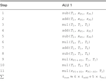
Typical operations during Phase 1 are the point operations point addition and point duplication.Table 3 shows the sequence of required computations for a point addition (withzP ¼1, as implemented for Phase 1). The operations for multiplication, addition and subtraction are denoted bymul,addandsub; the output operand is the first argument and the two input arguments are at the second and last positions.Tiare temporary registers. We identify at most two independent multiplication operations in this operation; i.e. before starting with multiplications 9 and 10, the results of the multi-plications from Steps 3 and 6 (and some additions and subtractions) have to be available.
Hence, at most two ALUs can significantly improve the execution time of Phase 1. Table 4 shows the parallelized sequence of the point addition for two ALUs. In Step 6 we can see ALU 1 running idle for the time of a multiplication since the point addition algorithm cannot be optimally parallelized. If we neglect
Table 3: Point addition with one ALU (pseudocode)
Step ALU 1 1 sub(T1,xP1,zP1) 2 add(T2,xP2,zP2) 3 mul(T3,T1,T2) 4 add(T1,xP1,zP1) 5 sub(T2,xP2,zP2) 6 mul(T4,T1,T2) 7 add(T1,T3,T4) 8 sub(T2,T3,T4) 9 mul(xP1þP2,T1,T1) 10 mul(T3,T2,T2) 11 mul(zP1þP2,xP1P2,T3) P
tsum6taddþ5tmul
Table 4: Point addition with two ALUs (pseudocode)
Step ALU 1 ALU 2
1 sub(T1,xP1,zP1) add(T4,xP1,zP1) 2 add(T2,xP2,zP2) sub(T5,xP2,zP2) 3 mul(T3,T1,T2) mul(T6,T4,T5) 4 add(T1,T3,T6) sub(T2,T3,T6) 5 mul(xP1þP2,T1,T1) mul(T3,T2,T2) 6 mul(zP1þP2,xP1P2,T3) P
the time for addition and subtraction, we can reduce the execution time by 40%. The number of temporary registers increases by 50% from four to six.
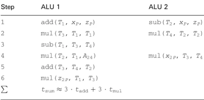
Tables 5 and 6 show the computations for a point duplication with one and two ALUs, respectively. Similar to point addition, we cannot manage an optimum parallelization since ALU 1 is running idle for some time.
The overall running time in the parallelized algorithm can be reduced by 40%; the number of registers required for intermediate results stays constant.
Phase 2, parameterized according to Section 4.1, is more complex to parallelize. All point operations can be
parallelized as described above. The computations for the product involve three multiplications, where two can be executed in parallel. Hence, an acceleration of35% can be achieved with two ALUs. (Remark: an improved acceleration of up to 50% could be attained by investi-gating a higher degree of optimization by interleaving parts of the operations.)
Combining both phases, two ALUs yield a total speed increase of 37%. Hence, the AT product of two ALUs is higher than that of a single ALU. Additionally, two more registers for intermediate values are required. However, considering the AT complexity of the entire ECM unit, the AT product does slightly decrease. The reason for this behaviour is the impact of the area due to the 21 registers of the unit. An additional ALU and two more registers only slightly influence the total area consumption, yielding a lower AT product.
Table 6: Point duplication with two ALUs (Pseudocode)
Step ALU 1 ALU 2
1 add(T1,xP,zP) sub(T2,xP,zP) 2 mul(T3,T1,T1) mul(T4,T2,T2) 3 sub(T1,T3,T4) 4 mul(T2,T1,A24) mul(x2P,T3,T4) 5 add(T3,T4,T2) 6 mul(z2P,T1,T3) P
tsum3taddþ3tmul
Table 5: Point duplication with one ALU (Pseudocode)
Step ALU 1 1 add(T1,xP,zP) 2 sub(T2,xP,zP) 3 mul(T3,T1,T1) 4 mul(T4,T2,T2) 5 sub(T1,T3,T4) 6 mul(T2,T1,A24) 7 mul(x2P,T3,T4) 8 add(T3,T2,T4) 9 mul(z2P,T1,T3) P