I M M I N P L P
U s i n g t h e N T C i n s i d e a p o w e r
e l e c t r o n i c m o d u l e
C o n s i d e r a t i o n s r e g a r d i n g t e m p e r a t u r e
m e a s u r e m e n t
A p p l i c a t i o n N o t e , V 1 . 0 , N o v . 2 0 0 9
Edition 2010-01-13 Published by
Infineon Technologies AG 59568 Warstein, Germany
© Infineon Technologies AG 2010. All Rights Reserved.
LEGAL DISCLAIMER
THE INFORMATION GIVEN IN THIS APPLICATION NOTE IS GIVEN AS A HINT FOR THE
IMPLEMENTATION OF THE INFINEON TECHNOLOGIES COMPONENT ONLY AND SHALL NOT BE REGARDED AS ANY DESCRIPTION OR WARRANTY OF A CERTAIN FUNCTIONALITY, CONDITION OR QUALITY OF THE INFINEON TECHNOLOGIES COMPONENT. THE RECIPIENT OF THIS APPLICATION NOTE MUST VERIFY ANY FUNCTION DESCRIBED HEREIN IN THE REAL APPLICATION. INFINEON TECHNOLOGIES HEREBY DISCLAIMS ANY AND ALL WARRANTIES AND LIABILITIES OF ANY KIND (INCLUDING WITHOUT LIMITATION WARRANTIES OF NON-INFRINGEMENT OF INTELLECTUAL PROPERTY RIGHTS OF ANY THIRD PARTY) WITH RESPECT TO ANY AND ALL INFORMATION GIVEN IN THIS APPLICATION NOTE.
Information
For further information on technology, delivery terms and conditions and prices please contact your nearest Infineon Technologies Office (www.infineon.com).
Warnings
Due to technical requirements components may contain dangerous substances. For information on the types in question please contact your nearest Infineon Technologies Office.
Infineon Technologies Components may only be used in life-support devices or systems with the express written approval of Infineon Technologies, if a failure of such components can reasonably be expected to cause the failure of that life-support device or system, or to affect the safety or effectiveness of that device or
AN2009-10
Using the internal NTC
Application Note 3 V1.0, 2009-11
AN2009-10
Revision History: 2009-11 V1.0
Previous Version: none
Page Subjects (major changes since last revision)
This Application Note replaces the AN2001-02 entitled Using integrated NTC with reliable isolation
We Listen to Your Comments
Any information within this document that you feel is wrong, unclear or missing at all? Your feedback will help us to continuously improve the quality of this document. Please send your proposal (including a reference to this document) to:
Table of Contents Page
1 Outline ... 5
2 Internal design ... 5
2.1 Isolation considerations ... 5
3 Considering the thermal situation for the NTC ... 6
4 Temperature measurement with NTC, analog approach... 8
4.1 Dimensioning R1 for the voltage divider ... 9
AN2009-10
Using the internal NTC
Internal design
Application Note 5 V1.0, 2009-11
1
Outline
One of the most critical parameters in power electronic devices is the chip temperature. A direct measurement however would require a sensor mounted on the chip or even being part of it. This would reduce the active area that contributes to the chip’s current carrying capabilities.
A viable alternative to determine the chips temperature is the calculation of the junction temperature using a thermal model and measuring the base plate’s temperature to have a known point to start from. In many of Infineon’s power electronic modules, thermistors, also known as NTC, are integrated as a temperature sensor to ease the design of an accurate temperature measurement.
The present application note deals with several topics related to isolation requirements, accessing the NTC and reading the temperature value from it.
2
Internal design
The NTC is mounted in close vicinity to the silicon chips to achieve a close thermal coupling. Depending on the module, the NTC is mounted either on the same DCB as the silicon or it may be mounted on a separate substrate:
NTC inside the EconoDUAL™ 3 mounted on a separate DCB close to the IGBT
NTC inside a module without baseplate, mounted close to the silicon
2.1
Isolation considerations
Independent from the NTC’s position, it is covered with the isolating gel that fills the module. In any regular operating condition, the isolation requirements are met. An isolation test is conducted during production according to the standard EN50187 to assure the isolation quality.
The standard defines several levels of isolation quality, differentiating in functional and reinforced isolation. Reinforced isolation, often required in inverter designs, is defined as:
An improved basic isolation with such mechanical and electrical properties that, in itself, the isolation provides the same degree of protection against electrical shock as double isolation. It may consist of one or more layers of isolation material.
Considering the thermal situation for the NTC In case of failure, the possibility exists, that a conducting path connecting the high voltage to the NTC may come to existence as hinted out in Figure 1:
Figure 1 Conducting path in case of failure
The path itself could be formed by moving bond wires that change their position during the failure event or by a plasma path forming as a consequence of arcing during failure.
For this reason, the isolation for the internal NTC only qualifies a functional isolation. In case reinforced isolation is required, additional isolating barriers have to be added externally.
Several methods have proven to be viable alternatives over the recent years, among them:
• Having the control designed with reference to the high voltage and add an isolation barrier between touchable parts and the whole control electronic
• Use analog amplifiers with internal isolation barrier to sense the voltage across the NTC
• Transfer the NTC’s voltage to a digital information that can be transported to the control by means of isolating elements like magnetic or optic couplers
Though in some applications a functional isolation for the NTC could be sufficient it should carefully be checked that all isolation requirements for the particular design are met.
3
Considering the thermal situation for the NTC
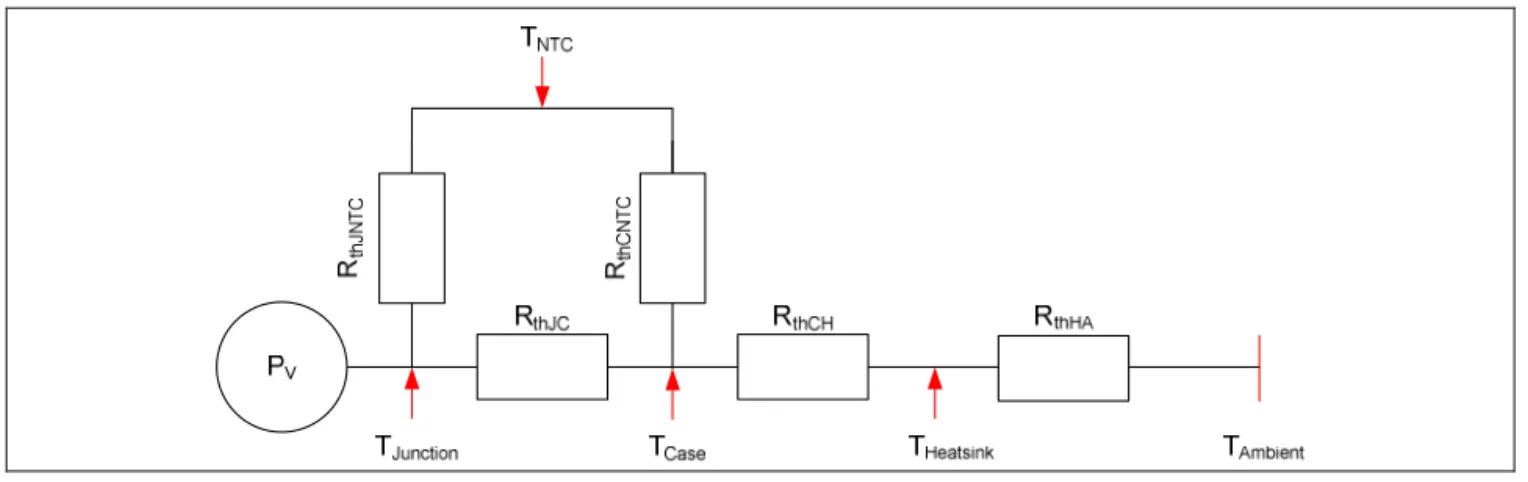
The NTC, mounted to a module’s DCB, is connected to thermal flow inside the module as briefly depicted in Figure 2:
Figure 2 Flow of thermal energy inside a power electronic module
The majority of heat generated in the chip flows directly to the heatsink from where it is dissipated to the environment. Additionally, heat flows through the DCB material and the baseplate towards the NTC’s position.
As heat does not flow instantaneously, the NTC is only suitable to represent the case temperature in static points of operation. Transient phenomena like heat generated in short circuit conditions can not be monitored or detected as the correlating time constants are far too small.
AN2009-10
Using the internal NTC
Considering the thermal situation for the NTC
Application Note 7 V1.0, 2009-11
An equivalent schematic representing the thermal situation and the possible pathes for the heat to flow is given in Figure 3
Figure 3 Equivalent thermal schematic From this overview, two conclusions can be drawn:
1. As there is a temperature drop along the path RthJNTC connecting the chip’s junction to the NTC, the
thermistor’s temperature TNTC has to be lower than the junction temperature TJunction
2. For the same reason, the temperature of the NTC has to be higher than the temperature that can be detected at the heatsink.
From experience, the difference between the heat sink’s temperature and the NTC’s temperature is about 10K at temperature levels common for power electronic devices.
Knowing the proper values for the Rth-chain is mandatory if temperatures that cannot be measured directly
are calculated from these values. For a given module, the according values for RthJC and RthCH can be read
from the datasheet for both the IGBT as well as for the diode. IGBT values
Diode values
Figure 4 Rth-Values as printed in Infineon’s datasheets for power electronic modules
With these values the thermal situation now can be calculated
(
)
K
R
P
T
K
T
T
R
R
R
P
T
R
P
T
T
R
P
T
T
R
P
T
T
R
P
T
T
H T thHA V amb H NTC thHA thCH thJC V amb th V amb J thHA V amb H thCH V H C thJC V C J10
10
~
+
=
+
⋅
+
+
+
⋅
+
=
⋅
+
=
⋅
+
=
⋅
+
=
⋅
+
=
∑
4
4 3
4
4 2
1
Temperature measurement with NTC, analog approach As the NTC only reflects the case temperature, it is sufficient to know the sum of losses and the module’s total RthCH that is given in the section “Modul / module” within the datasheet as well:
Figure 5 Rth-Value for a complete module as printed in Infineon’s datasheets
For more information about thermal modeling and calculation of thermal aspects please check the Infineon database for the application note AN2008-03 Thermal equivalent circuit models.
4
Temperature measurement with NTC, analog approach
This basic approach is based on a voltage divider with the NTC as a thermally sensitive device as shown in Figure 6:
)
(
)
(
1 1ϑ
ϑ
R
R
R
U
U
R+
⋅
=
Figure 6 Voltage divider utilizing the internal NTC
The charakteristic of the NTC is given in the datasheet in two different formats. A graphic representation R=f(ϑ) is given completed by parameters to analytically describe an approximation of the graph. The valid mathematical representation is
−
⋅
=
2 11 1 25
)
(
T TB
e
R
R
ϑ
with the parameters
K
T
k
R
K
B
3433
,
5
,
298
,
15
1 25
100 /
25
=
=
Ω
=
For a more accurate calculation, the datasheets also provide the values B25/50 and B25/80 in case only a
smaller temperature range is in focus.
With the voltage UR known through measurement, the actual resistance R(ϑ) can be calculated to be
R R
U
U
U
R
R
−
⋅
=
1 1)
(
ϑ
,leading to an expression for the actual temperature:
.
If a temperature value is wanted, the equation can easily be solved using a microprocessor that uses a digitized value of UR as an input.
If only a threshold signal for a maximum temperature is needed, a comparator that triggers at a predefined value is sufficient.
AN2009-10
Using the internal NTC
Temperature measurement with NTC, digital approach
Application Note 9 V1.0, 2009-11
4.1
Dimensioning R
1for the voltage divider
Choosing R1 needs to be done carefully to achieve a proper reading. If chosen too small, the flowing current
inside the NTC will lead to losses that in turn heat up the device thereby falsifying the measured results. If, on the other hand, R1 is chosen too large, the measured voltage gets too small and in turn the measurement
looses accuracy again.
To minimize the influence of the current, a thermal view is helpful. The thermal conductivity for the NTC is 145K/W. If a 1K influence is tolerable, the power dissipation inside the NTC may not exceed Pmax=6.9mW.
Assuming that a measurement up to 100°C needs to be done, the NTC will reach a value of R100=493Ω.
From this, the maximum current can be calculated to be
mA
R
P
I
3
.
74
100 max
max
=
=
.With a supply voltage U1=5V and a current limit of 3mA, the resistor R1 becomes
Ω
≈
−
=
100843
max 1
1
I
R
U
R
.As there is no such resistor, 910Ω can be chosen, leading to Imax=3.56mA; any value that limits the current to
I<4mA can be considered as long as 1K difference is tolerable.
5
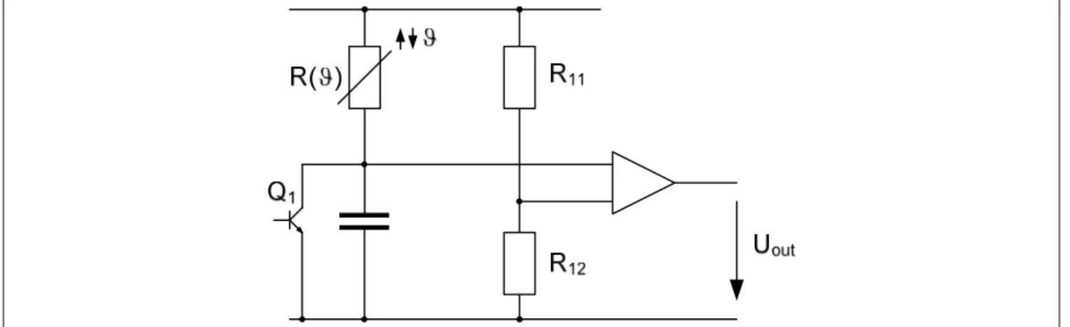
Temperature measurement with NTC, digital approach
Instead of using a voltage divider, the change of the NTC’s resistance over temperature is used to influence the time constant of an R-C-combination, a basic schematic is given in Figure 7.
Figure 7 Basic schematic to get a digital temperature information
The resistors R11 and R12 define the threshold for the comparator to change its output. The signal Uout is also
used to trigger the transistor Q1 to discharge the capacitor. As charging of the capacitor is defined by the
NTC’s resistance R(ϑ), Uout becomes a pulse pattern with a frequency fout=g(ϑ).
To reconstruct the actual temperature from Uout, it is sufficient to count pulses for a well defined period. The
number of pulses identifies the temperature; mapping pulses to temperatures can be done using an analytic description or a look-up table with interpolation between the two closest values.