Conducting AFM on graphene
THESIS
submitted in partial fulfillment of the requirements for the degree of
BACHELOR OF SCIENCE
in
PHYSICS
Author : Ruben van Erkelens
Student ID : 1437267
Supervisor : Jan van Ruitenbeek, Federica Galli
2ndcorrector : Thijs Aartsma
Conducting AFM on graphene
Ruben van Erkelens
Huygens-Kamerlingh Onnes Laboratory, Leiden University P.O. Box 9500, 2300 RA Leiden, The Netherlands
July 4, 2018
Abstract
This thesis deals with the use of conducting AFM to image the topography and conducting properties of graphene on SiO2. Specifically, the current image will be used to distinguish graphene from SiO2and the
height image to identify the edge of the wafer. These together can show how far graphene reaches this edge. For testing the usability of the Conducting AFM module measurements were also made on gold and on
Contents
1 Introduction 1
2 Theory 3
2.1 Graphene 3
2.2 Nanogap junction 5
3 Fundamentals of AFM 7
3.1 Atomic Forces 7
3.2 Principles of AFM 8
3.3 AC mode 10
3.4 Conducting AFM 12
3.5 Current preamplifier 13
3.6 Force/distance- and current/distance-curves 14
3.7 I/V spectroscopy 16
3.8 Quantitative Imaging mode 16
3.9 AFM probes 17
3.10 AFM setup 19
4 Results 21
4.1 AC Edge Measurements 21
4.2 QI Edge Measurements 22
4.3 CAFM on Gold/Mica 23
4.4 CAFM on Graphite 25
4.5 CAFM on Graphene/SiO2 27
4.6 QI CAFM Settings 34
Chapter
1
Introduction
A material that is 200 times stronger than steel, 1000 times lighter per square meter than paper, with a theoretical electron mobility 107 times higher than that of copper and being only one atom thick sounds very promising for many scientific purposes [1]. This material exists, and it is called graphene. Ever since its discovery in 2004 by Novoselov et al.[2], who won a Nobel prize for their work, physicists have recognized the po-tential of graphene and have done a considerate amount of research on it. The amount of articles published on graphene has been rising exponen-tially ever since its discovery.[3]
2 Introduction
Chapter
2
Theory
2.1
Graphene
Graphene is a two-dimensional material completely consisting of carbon atoms, structured in a hexagonal lattice, each 1.42 Angstrom apart, which originates from graphite. Graphite is way more common than graphene, it can be found in nature and it is a mineral crystalline form of carbon. Graphite is a layered material. Sheets of graphene themselves seldom break, and are even reported to be 200 times stronger than steel.[4] In graphite the layers are kept together by weak van der Waals bonds, there-fore they can be easily separated. One can make graphene by exfolia-tion, that is, by using sticky tape on graphite, taking a few layers off. Doing this over and over again can leave a few layers or possibly even one layer of graphene. This method was first reported to work by Geim and Novoselov, who successfully isolated graphene and characterized its properties, for which they won the Nobel prize in 2004.[2]
occu-4 Theory
pied states at zero temperature. A band with higher possible energy states exists, and is called the conduction band. Valence band and conduction band are separated by a band gap in which no states are possible. Metals have no band gap, and therefore have one band containing both occu-pied and unoccuoccu-pied states. At temperatures higher than zero, thermal energy can excite delocalized electrons, moving them up to a higher elec-tron state. This leaves an unoccupied lower energy state called a hole. Metals have no band gap, meaning that this can happen with relatively low energy excitations. Insulators have a band gap which is generally too great to overcome, meaning that electrons will not occupy higher energy states. Semi-conductors do have a band gap, but this band gap is rela-tively small. With an excitation energy that is great enough, the band gap can be overcome, moving an electron up to the conduction band. These excited electrons are referred to as free electrons and they are free to move through the material or fill up an existing hole. Free electrons will move in a certain direction once a bias voltage is applied, giving a current. The pos-sibility for flow of electrons is what makes a material conducting. Doping of a semi-conductor can further increase conductivity, by using impuri-ties with possible energy states in the energy range of the band gap of the semi-conductor.
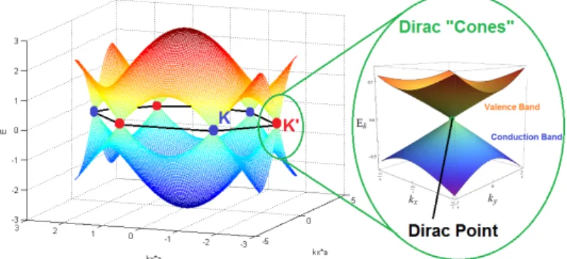
Figure 2.1:Dirac cones of graphene at six hexagonal separated points in a energy-momentum spectrum. Copyright: muonray
2.2 Nanogap junction 5
points gives a relation between energy and momentum by: E=±vF|p|[5] withEand|p|the energy and absolute momentum of the electron respec-tively andvF =8·105m/sthe Fermi speed. This formula has similar form as the relativistic formula for massless particles moving with the speed of light, where the speed of light c is replaced by vF. Thus, electrons near valence band to conduction band energy effectively behave as massless particles. A result is that graphene has a very high electron and hole mo-bility, theoretically 200, 000cm2V−1s−1, which is 107times higher than that of copper. Practically, this mobility is less due to the substrate on which the graphene lies. On SiO2substrates the theoretical limit becomes slightly less to 40, 000cm2V−1s−1.[6]
2.2
Nanogap junction
With electronics becoming smaller and smaller, one can imagine the im-portance of junctions at the nanoscale in electrical circuits. Nanogap junc-tions can also be used though for measuring the resistance of molecules by placing them in between the electrodes of the junction. Though nanogap junctions are often consisting of two metal electrodes, there are definitely reasons to look at graphene as a material for electrodes. Graphene is thin-ner than metals, making it possible to measure on smaller molecules. DNA being a good example, where graphene is thin enough to measure on each nucleotide individually, without the next nucleotide bothering the mea-surement, thus becoming a DNA sequencer. The process in which these graphene nanogap junctions are made, matters a lot for the quality of the junction. The graphene on the junctions of interest for this project were made with a process called Chemical Vapor Deposition (CVD).
6 Theory
Figure 2.2:Schematic view of two wafers with graphene (white) on top.[7]
Chapter
3
Fundamentals of AFM
3.1
Atomic Forces
An Atomic Force Microscope (AFM) measures the atomic Forces between a very sharp probe (AFM tip) and the surface of the sample to produce a high resolution image of the sample surface. Atomic forces are the short range interactions experienced as neutral molecules or atoms get close to each other. There are several atomic forces to consider. Firstly, there is the Coulomb repulsion force; as atoms get closer to each other, their respec-tive electrons will repel each other for having the same charge sign. The second force follows from the Pauli exclusion principle. The Pauli exclu-sion principle states that two electrons cannot occupy the same quantum state, this means that if two atoms are so close to each other that their elec-trons are almost overlapping each others orbitals. If a shell is full, no more electrons can be added, because then electrons would have the same state. The result is a repulsive force.
8 Fundamentals of AFM
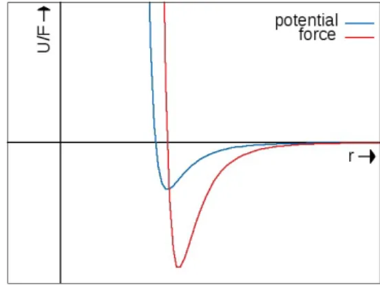
Molecules with more electrons will have a higher associated London dis-persion force. No permanent dipoles are needed for this interactions and therefore this interaction occurs with all molecules. All together, the forces approximately follow the Lennard-Jones potential
U(r) = ar−12−br−6
And the force, being its negative derivative, given as:
F(r) = −dU(r)
dr =12ar
−13− 6br−7
.
Here U is the potential, r the distance between two molecules or atoms and a and b two constants. Figure 3.1 shows what this potential and force looks like.
Figure 3.1:Lennard-Jones potential (blue) and its corresponding force (red)
From the point where the force goes from attractive to repulsive (soU
at a minimum), two molecules or atoms are said to be ”in contact”.
3.2
Principles of AFM
3.2 Principles of AFM 9
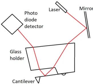
by using a laser and a photo diode detector. The laser points at the can-tilever, of which it reflects towards the photo diode detector, so when the cantilever deflects, the laser path will be different. Laser alignment is nec-essary each time a new tip is mounted or when the laser position is off due to thermal drift. The photo diode detector has four quadrants, each
quad-Figure 3.2:A laser reflects off the deflected cantilever onto a photo diode detector. From: https://www.doitpoms.ac.uk/tlplib/afm/cantilever.php
10 Fundamentals of AFM
force changes and therefore the position of the probe changes. Feedback corrects these changes depending on the mode used. The most classical mode for the AFM is contact mode, where the tip experiences an amount of force to make contact with the sample surface. The feedback does this by continuously changing the tip-sample distance so that the force remains constant. The changes are proportional to the topography of the surface, and therefore the height is mapped.[8] One might prefer contact mode for its simplicity, however there are definitely advantages to other modes. Some other modes and their advantages and features shall be discussed in the next sections.
3.3
AC mode
A common problem with contact mode is that the tip and sample both ex-perience high lateral and vertical forces, due to being so close to each other. This can severely damage the sample or make the tip blunt and distort the image. On biological/soft materials, the tip can damage or displace the sample. A solution is to oscillate the cantilever, making the tip come in contact only a short duration, and thus not exerting that much force over a long period of time. In standard AC mode the cantilever is oscillated around its resonance frequency with an amplitude which is large enough so that the tip will be in contact with the surface and then immediately out of contact again.
The cantilever can be represented by a driven, damped harmonic oscil-lator:
mx¨+cx˙ +kx =F0eiωt
withxthe displacement,mthe cantilever mass,cthe damping coefficient,
kthe spring constant of the cantilever,F0eiωt the driving force represented as a driving force amplitudeF0and a complex exponential dependent on angular frequencyω and time t. This equation can be solved for the am-plitude of the cantilever:
A(ω) = F0/m
[(ω20−ω2)2+4γ2ω2]1/2
withω0 =
√
3.3 AC mode 11
damping force, thus also increasing the damping factor γ. From the for-mula for the amplitude it can be seen that an increased damping factor results in lesser amplitude. The resonance frequency, which can be found by taking the derivative of the expression forAand setting to zero, yield-ingω2r = ω20−2γ2, decreases with increasing damping factor. Also, the phase difference between driving force and cantilever oscillation, given by φ = tan−1[( 2γω
ω02−ω2)], increases or decreases depending on the sign of the denominator as damping factor increases.[9] Differences in the ampli-tude and phase of the cantilever from those of the driving force are what is measured to make an image. The amplitude is used as a setpoint for feedback in AC mode. The described effect can be seen more clearly in figure 3.3.
Figure 3.3:Amplitude change and change in resonance frequency in the repulsive regime (tip in contact).[10]
be-12 Fundamentals of AFM
cause the contact time is too short and the Conducting AFM preamplifier is not fast enough to measure in this short time. More about this will be said in section 3.5.
3.4
Conducting AFM
3.5 Current preamplifier 13
3.5
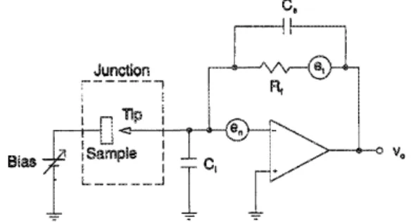
Current preamplifier
In CAFM, the output is very small (nA) current. This means a preampli-fier is needed to amplify and translate the current into voltages. A basic preamplifier circuit scheme for CAFM is given in figure 3.4[11] This is a so called trans-impedance amplifier and is similar/identical to the one used for Scanning Tunneling Microscopy (STM).
Figure 3.4:Circuit of a preamplifier used in CAFM.
At the left of this circuit, a bias is applied to the sample, if the condi-tions for CAFM are met, then a current will flow to the tip. The first nui-sance is in the form of a shunt parasitic capacitance, Ci. This capacitance comes from the wires from the tip to the preamp. This can be minimized by minimizing the distance from tip to preamp. The operational amplifier (opamp) in the preamp has a noise voltage source, en, depending on the characteristics of the opamp. There is a feedback resistor Rf b, and with it a parasitic shunt capacitance Cs associated to the resistor. Next in the circuit the thermal noise (Johnson noise),et, is given byet =
q
4kBTRf bf, it is caused by thermal motion of electrons in a resistor, withkBthe Boltz-mann constant,Tthe temperature, and f the frequency range. Finally, the preamp will give an output voltageVo. Its value depends on all the previ-ous components, however if one was to consider an ideal preamp without noise, the output voltage would be given by: Vout =−IinRf b. The current is amplified to a voltage by a factor of−Rf b, which is called the gain of the preamp.
14 Fundamentals of AFM
It is desired to have an as high as possible signal to noise ratio, yet a wide enough bandwidth range to measure in. The CAFM by JPK used for this thesis uses a value for the resistor of 108Ω, and has a bandwidth up to 1−2kHz.[13] Measuring with a frequency higher than the band-width frequency, will decrease significantly the output signal out of the preamplifier. This would be the case for AC mode, as the frequencies of the tips used to make high quality images in AC mode are much higher than 2kHz (usually around 70 or 300kHz). Also, to prevent tip wear, the tip in AC mode does not go very deep into the sample, meaning that it is in contact only very shortly. This makes AC mode suboptimal for CAFM, because the short contact and high frequency combination would give a very poor signal to noise ratio. Either contact mode or, as discussed in sec-tion 3.8, QI mode can be used, since they both measure in a low enough frequency range or slow enough.
3.6
Force/distance- and current/distance-curves
Force/distance-curves (F/d-curves) or current/distance curves (I/d-curves) can give a lot of valuable information. They describe how the force and current react as the tip comes closer to or moves away from the sample. An example of how a F/d-curve can look like is figure 3.5.
Figure 3.5:Force/distance-curve[14]
can-3.6 Force/distance- and current/distance-curves 15
tilever deflect by F = −kx. With an infinitely stiff sample, the decreased distance (which is not really a distance anymore as tip and sample are in contact) is completely compensated by the deflection (so the sample is not deformed/indented), the slope of the F/d curve then gives the spring con-stant of the cantilever. However, a realistic sample forms a spring as well, the decreased distance is compensated both by a deformation in the sam-ple and a deflection of the cantilever. The slope gives the combined spring constant. The force keeps increasing with decreased distance until a force setpoint is reached, after which the probe is retracted back. When retract-ing, starting at D, the behaviour is different from probe extend/approach as atomic and adhesion forces prevent that the tip comes out of contact, but eventually, when using enough force to retract, the tip will go out of contact. The adhesion forces are non-conservative and come from a wa-ter film which is always present on surfaces in ambient. The wawa-ter on the sample surface tends to stick around the tip and pull it down as it retracts, causing a bent of the cantilever. Using soft cantilevers will keep the tip in the water for a longer distance and if the water film is thicker, the adhesion forces will be higher. When getting sufficiently far away, so at E, the tip comes loose and it is out of contact (F).
Just like the force, the current is very much dependent on the distance from tip to sample. At great distance there is no current, the tunneling dis-tance is too large. However as the disdis-tance gets very small, say in the order of nanometers, a current will start to run, even though tip and sample are not in contact yet. This is the tunneling current, coming from the quan-tum mechanical nature of electrons, as they have a probability to cross the potential wall of the gap between tip and sample. Its current has an expo-nential dependence on the distance. The tunneling current is very small in comparison with the current when in contact but it can be measured by the preamp if set on a very high gain (108−109). It should be noted however that measuring the tunneling current can be difficult, because one would have to keep the tip sufficiently close the sample but not yet in contact.
16 Fundamentals of AFM
3.7
I/V spectroscopy
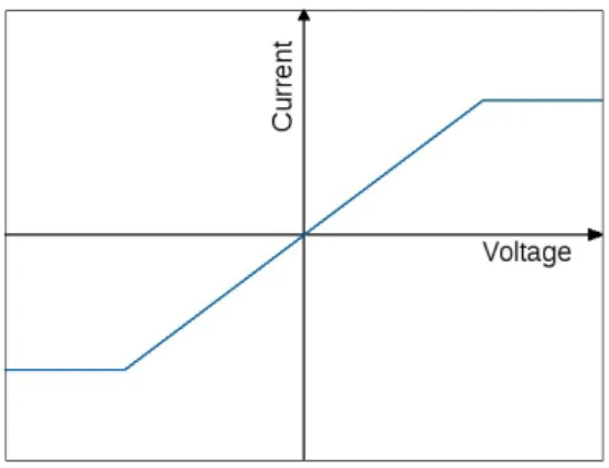
Once in contact, the force can be kept constant by the feedback in AFM mode∗. Now, changing the bias voltage will change the current. Mea-suring the current over a range of voltages is called current/voltage (I/V) spectroscopy. Figure 3.6 shows a typical I/V curve. The linear slope is di-rectly related to the resistanceRin case of Ohmic contact, which is essen-tially the resistance experienced from sample to tip. If the current exceeds the saturation level of the preamplifier the measured current becomes con-stant as soon as the saturation current is reached.
Figure 3.6:Example of an I/V spectroscopy curve. The curve is linear in the mid-dle and thus shows Ohmic behaviour. With increasing/decreasing voltage the measured current increases/decreases respectively until saturation of the pream-plifier is reached. The current will remain constant afterwards.
3.8
Quantitative Imaging mode
Quantitative Imaging mode (QI mode) is a relatively new mode intro-duced by the company JPK Instruments AG.[15] A JPK NanoWizard 3 was used for the experiments of this thesis, and so has QI mode been used for numerous measurements. In QI mode a force/distance-curve is made at every pixel. In order to do this, the tip has to cover a certain distance range at each pixel. Unlike AC mode, the cantilever of the probe is not driven to oscillate. It is in fact the whole tip holder that is moving up and down at lower frequency (max. 2kHz). Just like how F/d-curves are normally
∗Note that this is different than STM-spectroscopy. In this case the feedback is
3.9 AFM probes 17
made, the probe extends until a force setpoint is reached. At which dis-tance this setpoint is reached, is then translated to be the height of the im-age. The probe goes back to the retracted position, moves towards another pixel, and measures again. Repeating for each pixel in a raster results in an image. Imaging with QI does usually take slightly longer than imaging with tapping mode or contact mode, because of the time it takes to make a force/distance curve at each pixel. With this slow pixel taking, comes a low measuring frequency. This makes it ideal for doing CAFM, because the frequency is nicely in the range of the bandwidth of the preamplifier and therefore the preamplifier has enough time to perform an accurate current measurement for each given pixel. Of course, contact mode CAFM could also be used, however QI CAFM does not have the disadvantages of high lateral and vertical forces, because it is only temporarily in contact at every pixel. Contact mode is known to cause much high tip wear of the conducting coating.
3.9
AFM probes
The choice of probe can make a significant impact on image quality. In this section, different kinds of probes will be covered. AFM probes con-sist of a chip, with a cantilever attached to it. This cantilever should be reflecting when using a laser spot as measuring tool. At the end of the cantilever is a tip. Tips can have a pyramidical or hemispherical shape, depending on the type/manufacturing, or irregular/not defined shape. One can imagine that a probe with a sharp tip will make an image with a higher resolution than one with a blunt tip, as the resolution is very much determined by the tip radius. Probes can furthermore vary in resonance frequency, dimensions, stiffness, and material. Most probes are made out of silicon or silicon nitride. On different samples and in different modes, different probes are optimal for use.
In contact mode, the cantilever should be quite soft, so with a low spring constant. A cantilever high spring constant would apply a lot of force on the sample, which could damage it or viceversa, on a hard sam-ple the tip apex would become more and more blunt. The resonance fre-quency is low, as can be seen from the formula for a harmonic oscillator:
18 Fundamentals of AFM
In AC mode, it is often beneficial to use cantilevers with a higher res-onance frequency (about 70−300kHz). This can mean a high spring con-stant, but it depends on the material choice. High frequency (stiff) can-tilevers experience less negative effects from adhesion, as the cantilever would go in and out of the water film present in ambient air during AC mode, the high spring constant would make the cantilever push through the water more easily. In AC mode, the frequency of the cantilever also greatly influences the scanning speed as the resonance frequency is di-rectly linked to the measuring frequency.
The choice of probe in QI mode is not as significant as it is in tapping mode, as most probes can be used for height imaging purposes. However, one might want to avoid very soft tips when measuring in very humid conditions, because as said before, they suffer more from adhesion. This adhesion can dominate the whole F/d-curve, giving a qualitatively bad pixel. Also, the cantilever experiences a small oscillation as the tip shoots out of the water, this is called mechanical ringing. Oscillations are of big-ger amplitude when soft, low frequency cantilevers are used, but stiff can-tilevers might keep oscillating for a longer time. As for all modes, there should also be looked at the material one is measuring, as soft samples get damaged more easily by a probe with a high spring constant than hard samples do.
3.10 AFM setup 19
3.10
AFM setup
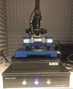
Every AFM apparatus is different in the details, but all AFMs have con-ceptually many of the same components. The AFM setup shall here be explained with figure 3.7, which is the AFM by JPK used for this thesis.
Figure 3.7:AFM setup
20 Fundamentals of AFM
Figure 3.8:Laser path in the AFM
Chapter
4
Results
In this chapter AFM measurements will be shown and discussed. That is, firstly, measurements on the edge of a graphene/Si/SiO2 sample, both in AC and QI, without CAFM. Then, CAFM measurements on different ma-terials, such as Gold on Mica, graphite, and graphene on Si/SiO2. Also, the different settings for optimizing CAFM imaging will be discussed with the help of images. A graphene/Si/SiO2 sample was used with a SiO2 thick-ness of 290nm, as this improves the optical visibility of the sample[18].
4.1
AC Edge Measurements
As for the general goal of this project, the measurement on the edge of a sample is quite important. In the AFM image it should be possible to see a clear macroscopic drop of what should be the edge. For this particular set of measurements, a graphene on Si/SiO2 wafer was used, similar to the one used in the nano junction. Firstly, the edge is measured with AC mode. A typical result can be seen in figure 4.1.
22 Results
Figure 4.1:AC edge measurement. The left is the AC height image, the right is the height change over the drawn line. The image was made on a graphene/Si/SiO2
wafer, with a209kHzsilicon tip.
downwards, instead of starting beyond the edge and onto the sample, as in this case the tip will bump into the sample edge, and as the edge is higher than 6.5µm, the tip will crash and get damaged.
4.2
QI Edge Measurements
Figure 4.2: QI edge measurement on a graphene/Si/SiO2wafer with a straight
drop off. Tip (209 kHz) and sample are similar as in figure 4.1.
4.3 CAFM on Gold/Mica 23
in figure 4.2. Both QI and AC images look very similar and are both able to measure the edge effectively.
4.3
CAFM on Gold/Mica
All further shown figures and measurements with CAFM were measured with RMN-25Pt300B tips[17], which have a characteristic resonance fre-quency of 20kHz. For testing the usability of CAFM, a sample of gold on mica∗was used. Gold is a well known conductor. Taking that into account, and the consideration that the gold film did not show cracks and is con-tinuous allover the substrate, whereas graphene might leave gaps, makes it so that gold is a promising material for testing the CAFM module.
As F/d, I/d-curves would show, figure 4.3, current could be measured on this material, though its values would differ significantly, to the point of not being measured at all. The maximum/minimum current which could be measured is +/- 12nA, which is the saturation level of the preamplifier, which means that the actual currents going through the tip were higher than this value when saturated. The inconsistency in current measure-ments could be explained by the tip having to make a clean contact with the sample surface, which is not always realized everywhere on the tip, because of adsorbates forming on the tip and on the gold. During mea-surement the tip can both lose or gain adsorbates as the tip moves over the surface during imaging, or penetrates the surface during an F/d, I/d-curve. In the case of the left graph in figure 4.3, the current shoots up to saturation right after contact was reached, meaning that the tip makes a relatively clean contact with the gold.
When it comes to imaging gold, one would expect to see atomically flat terraces at which the gold is raised up slightly higher or lower. This is a characteristic structure for Au(111) surface on mica substrates. In figure 4.4 one can see these terraces more clearly.
Also, a current image was made, where it is visible that there is more current measured at spots where there is a slope in height. An explanation can yet again be found with the contact area between the tip and the sam-ple; a flat surface will only be in contact with the very end of the tip, while a slope will be in contact with the sides of the tip as well. There might even be contamination on the end of the tip, while the sides of the tip are clean. The gold sample which was used has been in air for several weeks,
∗Mica is an insulating mineral which, similar to graphite, can be easily cleaved in
24 Results
Figure 4.3: A set of three F/d, I/d CAFM measurements,Vb = −10V (a voltage
4.4 CAFM on Graphite 25
Figure 4.4: QI CAFM measurement on gold, Vb = 1.108V. Left: Height image
showing terraces of gold. Right: Current image. More current is measured at black gaps in the height image, due to the change in height at these spots. The current in this image is very small, just1.4pAmax. Contamination is a possible explanation for this small current.
meaning that many adsorbates have formed on top of it, making it hard to measure current. This explains the rather low value of current measured.
4.4
CAFM on Graphite
By taking a sticky tape, and removing the top layers of a graphite sample, a new clean surface is created. The sample surface is now clean and less contaminated. This means that there should be current measured allover the sample. Typical for graphite are its steps in which a layer goes one or more atomic layer higher. Figure 4.5 shows an example of two such steps. One step of 5nm, which indicates that the step increases in several layers, and one step which can hardly be seen at first sight. Last step increases about 0.3nm in height, which compared to the theoretical 0.335nm inter-layer distance[4], means that this could be an increase of just one inter-layer. The current at a step is higher due to the slope of the step, increasing con-tact area. The bigger step has a bigger concon-tact area, thus higher current than the small step. This is confirmed by the measured current peaks of 5nAand 2nAof big and small step respectively, as seen at the bottom right graph of figure 4.5.
26 Results
4.5 CAFM on Graphene/SiO2 27
before the tip is even close. This happened often because it is quite easy to pick up flakes while scanning on graphite.
Figure 4.6: F/d, I/d curve on graphite,Vb = 0.608. The current increases way
before the tip reaches contact with the graphite, could indicate that a flake is at-tached on the tip.
4.5
CAFM on Graphene/SiO
2It is apparent that it is very well possible to make proper CAFM images, though it remains the question whether the method is applicable on graphene for the purpose of this project and what is the resolution of CAFM. One problem of graphene which is not present with graphite is that the graphene should be allover from the place where the bias is connected to the loca-tion where the tip lands. Graphene being a mono layer material can show discontinuities and cracks in several places. This is also the case for full coverage graphene. A sample with a relatively uncracked surface would be optimal. Another disadvantage of measuring on graphene in compar-ison to graphite is that it is obviously not possible to take off a top layer with sticky tape, and therefore the graphene sample should be very clean from the start and should be kept at vacuum to avoid adsorbates to form on the surface.
28 Results
and material thickness. A SiO2 thickness of 280−300nm was shown to be optimal for visible light.[18] One can imagine that a monolayer mate-rial can otherwise be hard to see and find, yet it can be very beneficial for experiments if one could locate the graphene prior to measuring. The improved visibility would prove useful for locating the boundary from graphene to SiO2 with an optical microscope before measuring on this boundary. This can be seen in figure 4.7.
Figure 4.7: An optical picture of the tip and the sample made with yellow light. The graphene can be seen in principle optically due to the chosen SiO2thickness
of290nmof the sample. The SiO2 appears as plain yellow while the graphene is
slightly darker and more patchy. In fact what helps the most here to see graphene is the defects and folds which are present in this graphene prepared in this way. By spotting this the boundary from graphene to SiO2 can be found. The RMN
probe has a tip that bends off downwards, as can be seen as a black ”pigeon” in the middle of the picture. On the far left a part of the tip holder is visible in dark black.
The graphene appears as darker and patchy, the SiO2 shows no char-acteristics and is plain yellow through the microscope.
im-4.5 CAFM on Graphene/SiO2 29
Figure 4.8:I/d curves of preamplifier noise. Left: Before the preamplifier modifi-cation. The noise has an impact of approximately0.8pA. Right: After the pream-plifier modification. The noise has an impact of appromixately6pA, meaning that the noise has increased with a factor 7.5 due to a factor 50 gain resistor decrease.
30 Results
poses more noise. Comparing the noise in the F/d, I/d-curve of the new preamp settings with the old preamp settings shows that there is a signif-icant change in noise, but the noise with the new preamp settings is still just in the range of a few pA, which does not matter when measuring on currents in the range ofnA, as seen in figure 4.8.
I/Vs on graphene, figure 4.9, show that the current can reach the sat-uration level of +/- 600nAwith the new preamp, at about +/- 0.5V away from the offset voltage of −0.108V. In the I/V with the old preamp set-tings, the current reached saturation as shortly as 0.04V away from the offset. This is not a factor 50 apart, which is because the resistance ex-perienced by the current is different in both I/Vs. This could have been calibrated using a known resistor. The resistances in both images, as can be received by the slope byV = IR, are 276kΩand 889kΩfor left I/V and right I/V respectively.
To interpret these values, an estimate of what can be expected for the resistance and current on graphene was made. The total resistance of the system can be seen as a sum of the resistance of the point contact between tip and substrate, and the resistance of the substrate between tip and lo-cation on the substrate where the bias is applied. The latter being negli-gible for the thick and well conducting gold and graphite substrates, but graphene is atomically sharp, so this resistance should be taken into ac-count. Taking a homogeneous resistivity ρ, the resistance of an Ohmic resistance can be calculated by the formula
R =
Z l2
l1
ρ
A(l)dl
with l1 and l2 the starting and ending lengths as seen from a reference point, and A(l) the cross sectional area dependent on length. In the par-ticular case of a sheet of graphene, the resistance can be calculated with circular sections, where each circular section has radius l, width dl, and thicknesst. The sections are in series, and can thus be calculated by inte-grating overdl. The area is given by A(l) = 2πlt. Then, using the defini-tion for sheet resistanceRs =ρ/tand filling in the area, the expression for
Rbecomes:
R= Rs 2π
Z l2
l1
dl l
4.5 CAFM on Graphene/SiO2 31
can be estimated asl1 ≈1cm. The sheet resistance for graphene was taken asRs =1840Ω≈2·103Ω[19]. Filling in then gives R=3kΩ.
To complete the estimate, the resistance from the point contact is added, which can be seen as a contact of an individual atom. For one atom this is the quantum resistance R = 2he2 ≈ 13kΩ[20]. It is here assumed that a one atom contact is made, but it should be noted that this might not be the case for a tip pushed into a sample. Adding up the estimate for the sheet graphene and the point contact givesR =2·104Ω. Comparing this estimate with the results from figure 4.9 gives that the estimate is 17 and 56 times smaller than the resistances of 276kΩand 889kΩof left and right curve respectively. A voltage ofV = 0.5V corresponds to saturation cur-rent, 600nA, for the right curve, but would give a current of 3·102Ausing the estimate.
There are several possible explanations for the difference in estimate and measurement. Firstly, the chosen value for the sheet resistance could have been different from that of the measurements. The sheet resistance varies strongly depending on the state of the graphene used, because the amount of cracks and adsorbates could be different in every graphene sample. Secondly, the chosen lengths were estimated very roughly, es-pecially the radius of the tip. However, the terms for length are in a log-arithm after evaluation of the integral for resistance over circular sections and so differences in the chosen lengths will only matter little.
Finally, images on the boundary from graphene to SiO2 were made. Some of the CAFM images of the graphene to SiO2 transition are shown in figures 4.10 and 4.11. The transition is clearly visible in both the current image and the height image. In the conducting image current is measured on the graphene and then suddenly stops, thus when reaching SiO2.
Another way to check whether or not this is the transition is by look-ing at the height increase when golook-ing to graphene. Figures 4.10 and 4.11 show a height increase of near and about 2nm. This is not in accordance with the theoretical 0.335nm[4], for this should be the thickness of a sin-gle graphene sheet. The reason could be air and water molecules which are trapped under the graphene sheet. During the creation process of the graphene/Si/SiO2wafer, the graphene sheet was laid on top of the SiO2, however there might have been molecules on the SiO2 which could not escape. This adds to the measured height difference. 2nm is actually a height difference more often measured with AFM on graphene.[21]
32 Results
Figure 4.10: QI CAFM measurement on graphene made after the preamp modi-fication. Vb = 0.108V,sp = 92nNLeft: A topography image where the top half
has a part which is slightly higher than the rest of the image. Middle: Current image. The upper part is graphene, as current is measured there, whereas no cur-rent is measured on SiO2. On the right side of the current image there appears
to be no/little graphene, which is also visible in the height image. Right: Two height differences of around2nm, with a small peak which could be contamina-tion. black: 1 red: 2
Figure 4.11:QI CAFM measurement on graphene after the preamp modification.
Vb = 0.108V, sp = 92nN Left: Topography image. The upper part is slightly
higher. Middle: Current image. The upper part is graphene as seen in this cur-rent image. No curcur-rent is measured on the bottom part. Right: Some height dif-ferences in the graphene to SiO2 transition. The differences are around1−3nm
4.5 CAFM on Graphene/SiO2 33
goes up one line. During this process the tip could lose or gain some dirt, thus explaining a streaky pattern. The high increase in current in figure 4.11 could be explained by a loss of a relatively high amount of dirt from the tip. With current above saturation level, further small loss or gain of dirt of the tip will remain unmeasured and no streaky pattern is seen. On the right side of figure 4.10 there appears to be little or no graphene. The graphene seems to be damaged there, which could possibly have been caused mechanically by the tip during measurement.
Figure 4.12:QI CAFM measurement made before the preamp modification.Vb= 0.608V,sp= 120nNLeft: Topography image. Middle: This current image seems quite similar to the height image but for one part which is not ”recognized” in the current image. This could be an island of graphene loose from the bulk. Therefore this island was not in contact with the bias. Right: Height over the line drawn in the height image. A clear gap is visible, giving a distance between bulk and island of around0.2−1µm.
In these images it is possible to recognize graphene just in the topog-raphy image. This is also the case in figure 4.12, however in this image a feature in the middle of the image is visible where the height image shows an island next to the bulk graphene. This cannot be SiO2 as this is typi-cally flat, nor does it look like contamination. It could be a graphene island which is loose from the bulk. In this way there is no electrical contact with the island, therefore no current is measured on it.
34 Results
and 4.2. The CAFM module should be able to show the graphene to SiO2 transition together with an edge measurement.
However this measurement was not done, because samples degraded rapidly due to increasing contamination and adsorbates. Even when stored in vacuum, current on graphene appeared to be unmeasurable in a times-pan of four weeks. Note that samples were stored at about 1mbar, so not in high vacuum.
4.6
QI CAFM Settings
Lastly, optimal settings will be discussed for measuring on graphene with the CAFM module. Settings were tested by making images with different settings and comparing them.
A setting that can make a significant change to a current image is the bias voltage. The bias voltage can be set from−10V to 10V, though volt-ages this high can destroy the tip, which makes sense as a too high current will go through a tip of a few nanometers radius. Also, a voltage that is too high will mostly show either saturation level of current at conducting spots or no current at all at non-conducting spots. For seeing more detail in images, one would want to see a wide range of different currents all through the image, so that different areas can quantitatively be compared. A low voltage serves this purpose well, however using a lower voltage results in a current relatively smaller to noise levels. Figure 4.13 show sev-eral used voltages of 0.008V, 0.108V and 0.308V. Even at the lowest volt-age of 0.008V, the pattern can be seen. This voltage is arguably enough, though a voltage a bit higher, such as 0.108V, can show differences more clearly. Voltages of 0.308V appear to be unnecessary, but also to change both current and topography image. Figure 4.13 shows a strongly chang-ing topography image on subsequent measurements, which is possibly caused by the tips movement during measurement. The current images show a streaky pattern similar as in figure 4.11, which could again be caused by losing and gaining dirt on the tip visible in the current in lower current images. In the second to third current image there is an increase in voltage applied, yet a decrease in current measured. This could yet again be explained by the loss or gain of dirt on the tip, as the amount of dirt could change while measuring on SiO2as well.
4.6 QI CAFM Settings 35
Figure 4.13:QI CAFM measurement on graphene,sp =90nN. Top: Topography images. Bottom: Current images. From left to right:Vb=0.008V,0.108V,0.308V.
Figure 4.14:QI CAFM measurements on the same spot of graphene with increas-ing force setpoint. Vb = 0.108V. Top: Topography images. Bottom: Current
36 Results
Figure 4.15: QI CAFM measurements on graphene taken right after each other.
Vb=0.108V,sp=92nNLeft: Initial topography and current image, the graphene
is clearly visible in both images. Right: Topography and current image taken right after the first one. Many graphene spots seemed to have disappeared, so graphene is being damaged.
4.7 Conclusion 37
the graphene at 100nN. For this reason, setpoints used during this project for doing CAFM were mostly around the 90nNor 100nN, which are quite high. Note that at around 100nNgraphene starts to get damaged.
Though these tests make it seem that force setpoints with such high forces are optimal, many measurements would rise the suspicion that the force used was too high. Figure 4.15 shows two height and current images made just two minutes after each other with a force setpoint of 92nN. Both in the height image and the current image it appears as if the graphene has changed significantly. This was more frequently observed in subsequent images while using these specific settings, regardless of which voltage. It could be caused by the tip pushing too heavily onto the graphene sur-face, changing its topography (damaging/cutting) while doing so. Espe-cially since this occured at the end of a graphene sheet, where graphene will have more defects[22] than in the middle of a sheet, which makes it weaker.
4.7
Conclusion
Knowing about this damaging effect, it would seem as if CAFM on graphene is really suboptimal, as it is possible to measure current on graphene and identify graphene, but only when such a high force is used so that the graphene itself changes, making measurements qualitatively a lot worse. The high force causes damage at the edges where it is more weak. This is a drawback, but it can be used to ”cut” graphene by AFM nanolithography. At the root of this problem lies a deeper issue. The reason that such a high force setpoint had to be used, was that the tip would have to push through contamination and adsorbate layers. Tip/sample contamination is a big drawback, as measurements would more often than not show no current in current images/curves. This proved to become more of an is-sue when samples were stored for longer, increasing the period in which the sample was exposed to air, thus increasing contamination. Using high forces would to some extend solve the problems of contamination, but im-pose other problems as mentioned above. Using fresh/new samples and recently cleaned tips (tips could be cleaned by argon etching for example) could decrease the amount of contamination. Also, improvements could be made by measuring in a more controlled atmosphere and storing the samples in a better vacuum (samples during this project were stored in a 1 mbar vacuum).
38 Results
For further research on CAFM, one might want to try using Si or SiN tips coated with conducting (doped) diamond or metal carbides or Tita-nium.
Acknowledgements
Bibliography
[1] graphenea.com.
[2] K. S. Novoselov, A. K. Geim, S. V. Morozov, D. Jiang, Y. Zhang, S. V. Dubonos, I. V. Grigorieva, and A. A. Firsov, Electric Field Effect in Atomically Thin Carbon Films, Science306, 666 (2004).
[3] https://www.researchtrends.com/issue-38-september-2014/graphene-ten-years-of-the-gold-rush/.
[4] C. Lee, X. Wei, J. W. Kysar, and J. Hone, Measurement of the Elastic Properties and Intrinsic Strength of Monolayer Graphene, Science 321, 385 (2008).
[5] http://www.physics.upenn.edu/ kane/pedagogical/295lec3.pdf.
[6] J.-H. Chen, C. Jang, S. Xiao, M. Ishigami, and M. S. Fuhrer, Intrin-sic and extrinIntrin-sic performance limits of graphene devices on SiO2, Nature Nanotechnology3, 206 (2008).
[7] A. Bellunato, S. D. Vrbica, C. Sabater, E. W. de Vos, R. Fermin, K. N. Kanneworff, F. Galli, J. M. van Ruitenbeek, and G. F. Schneider,
Dynamic Tunneling Junctions at the Atomic Intersection of Two Twisted Graphene Edges, Nano Letters0, null (0), PMID: 29513997.
[8] P. E. West,Introduction to atomic force microscopy theory, practice, appli-cations, (2007).
40 BIBLIOGRAPHY
[11] T. Tiedje and A. Brown, Performance limits for the scanning tunneling microscope, 649(1990).
[12] C. J. Chen and W. F. Smith, Introduction to scanning tunneling mi-croscopy, American Journal of Physics62, 573 (1994).
[13] J. Instruments,JPK Conductive AFM (CAFM) module for NanoWizardR
AFM, page 1.
[14] V. Shahin, W. Hafezi, H. Oberleithner, Y. Ludwig, B. Windoffer, H. Schillers, and J. E K ˜AŒhn,The genome of HSV-1 translocates through the nuclear pore as a condensed rod-like structure, 119, 23 (2006).
[15] J. Instruments,Quantitative Imaging with the NanoWizard, page 1. [16] C. Science and N. Sciences, Atomic Force Microscopy - An advanced
physics lab experiment, (2014).
[17] Rocky Mountain Technology, LLC. http://rmnano.com/index.html.
[18] P. Blake, E. W. Hill, A. H. Castro Neto, K. S. Novoselov, D. Jiang, R. Yang, T. J. Booth, and A. K. Geim,Making graphene visible, Applied Physics Letters91(2007).
[19] S.-a. Peng, Z. Jin, P. Ma, D.-y. Zhang, J.-y. Shi, J.-b. Niu, X.-y. Wang, S.-q. Wang, M. Li, X.-y. Liu, T.-c. Ye, Y.-h. Zhang, Z.-y. Chen, and G.-h. Yu, The sheet resistance of graphene under contact and its effect on the derived specific contact resistivity, 82, 500 (2015).
[20] C. J. Muller, J. M. van Ruitenbeek, and L. J. de Jongh,Conductance and supercurrent discontinuities in atomic-scale metallic constrictions of vari-able width, Phys. Rev. Lett.69, 140 (1992).
[21] M. K. Blees, A. W. Barnard, P. A. Rose, S. P. Roberts, K. L. McGill, P. Y. Huang, A. R. Ruyack, J. W. Kevek, B. Kobrin, D. A. Muller, and P. L. McEuen,Graphene kirigami, Nature524, 204 (2015).
![Figure 2.2: Schematic view of two wafers with graphene (white) on top.[7]](https://thumb-us.123doks.com/thumbv2/123dok_us/8161654.2163833/12.892.301.650.193.375/figure-schematic-view-wafers-graphene-white.webp)

![Figure 3.3: Amplitude change and change in resonance frequency in the repulsive regime (tip in contact).[10]](https://thumb-us.123doks.com/thumbv2/123dok_us/8161654.2163833/17.892.127.419.493.721/figure-amplitude-change-change-resonance-frequency-repulsive-contact.webp)
![Figure 3.5: Force/distance-curve[14]](https://thumb-us.123doks.com/thumbv2/123dok_us/8161654.2163833/20.892.189.475.705.914/figure-force-distance-curve.webp)