Coupling light to periodic
nanostructures
Coupling light
to
periodic nanostructures
Proefschrift
ter verkrijging van
de graad van Doctor aan de Universiteit Leiden,
op gezag van Rector Magnificus prof. mr. P. F. van der Heijden, volgens besluit van het College voor Promoties
te verdedigen op donderdag 24 september 2009 klokke 13:45 uur
door
Eduard Frans Clemens Driessen
Promotor: Prof. Dr. J. P. Woerdman Universiteit Leiden Copromotor: Dr. M. J. A. de Dood Universiteit Leiden Leden: Prof. Dr. G. W. ’t Hooft Philips Research/
Universiteit Leiden Dr. Ir. H. L. Offerhaus Universiteit Twente Prof. Dr. M. A. G. J. Orrit Universiteit Leiden Prof. Dr. J. M. van Ruitenbeek Universiteit Leiden
The work presented in this thesis has been made possible by financial support from the Dutch Organization for Scientific Research (NWO) and is part of the scientific program of the Foundation for Fundamental Research of Matter (FOM).
Contents
1 Introduction 1
1.1 Periodic nanostructures . . . 2
1.2 Bound modes in slabs and at surfaces . . . 3
1.2.1 Waveguide modes . . . 4
1.2.2 Surface plasmons . . . 5
1.3 Periodic guiding structures . . . 6
1.4 This thesis . . . 8
1.5 Polarization convention . . . 9
Part I - Photonic-crystal slabs 11 2 Fano resonances and waveguide modes in a two-dimensional photonic-crystal slab 13 2.1 Introduction . . . 14
2.2 Photonic crystal fabrication . . . 14
2.3 Theory . . . 17
2.3.1 Fano model . . . 17
2.3.2 Waveguide modes . . . 20
2.4 Reflection measurements . . . 24
2.5 Conclusion . . . 26
3.2 Experiment . . . 28
3.3 Model . . . 29
3.4 Conclusion . . . 32
4 Imaging of a Fano resonance in a two-dimensional photonic-crystal slab 33 4.1 Introduction . . . 34
4.2 Sample . . . 34
4.3 Normal-incidence reflection spectrum . . . 35
4.4 Imaging of the resonance . . . 37
4.4.1 k-space imaging and polarization properties . . . 38
4.4.2 Real space imaging . . . 40
4.5 Conclusion . . . 44
Part II - Metal hole arrays 45 5 Enhanced coupling between plasmons in hole arrays with pe-riodic dielectric antennas 47 5.1 Introduction . . . 48
5.2 Experiment . . . 49
5.3 Coupling to surface plasmons . . . 50
5.4 Coupling between surface plasmons . . . 53
6 Waveguide modes in solid-state index-matched metal hole ar-rays 55 6.1 Introduction . . . 56
6.2 Waveguide modes . . . 56
6.3 Effects of layer thickness . . . 59
6.4 Conclusion . . . 62
7 Observation of coupling between surface plasmons in index-matched hole arrays 63 7.1 Introduction . . . 64
7.2 Experiments . . . 64
7.3 Model . . . 67
7.4 Conclusion . . . 73
Contents
8 Polarization-dependent optical absorption of superconducting
single-photon detectors 77
8.1 Introduction . . . 78
8.2 Experimental setup . . . 79
8.3 Characterization . . . 81
8.4 Polarization dependence . . . 84
8.5 Discussion . . . 88
8.5.1 An optical impedance model for the absorption . . . 88
8.5.2 The effect of film thickness . . . 89
8.5.3 Illuminating through sub- or superstrate . . . 91
8.6 Conclusion . . . 92
9 The perfect absorber 95 9.1 Introduction . . . 96
9.2 Absorption of a closed film . . . 96
9.3 Nanostructured films . . . 99
9.4 Conclusions . . . 101
Appendix 103 A Fabrication recipe for photonic-crystal slabs 105 A.1 Wafer preparation . . . 105
A.2 Mask definition . . . 106
A.3 Pattern transfer . . . 106
A.4 Mask removal . . . 107
A.5 Membrane formation . . . 107
Bibliography 109
Summary 119
Samenvatting 123
Curriculum Vitæ 127
Chapter 1
Introduction
Already since ancient history, mankind has tried to manipulate light and use it for their purpose. The fact that a piece of glass can be used to manipulate light was known by the ancient Greeks, as reports Aristophanes in his comedy “The Clouds” [1], first performed in 423 B.C.:
Strepsiades You know in a chemist’s shop... that round thing...
clear, like a pretty stone you can see right through... For fires...
Socrates You mean a magnifying glass?
Strepsiades That’s it. I’ll take one with me in court... Stand
behind the clerk with the wax tablets... And when he writes down the fine, melt it away.
Socrates That’s clever. I like it.
Ever since then, a better and better understanding of light went hand in hand with new inventions, that marked new eras of using and manipulating light. The microscope made it possible to look at ever smaller objects, and the in-vention of the laser marked the era of using light as an information carrier. A final step was made with the advent of nanotechnology. This technology made it possible to structure materials on a scale of hundreds of nanometers, smaller than the wavelength of light.
On the other hand, a technology-centered route was taken. Plasmonics has taken a renewed interest, because of its promise to focus light on a nanome-ter scale [10], and multitudes of nanostructures were conceived to steer and guide light [11]. The strong wavelength dependence of several resonant effects inspired people to make photon sorters [12], and the sensitivity for minute changes in refractive index paved the way for nanostructured sensors [13].
1.1
Periodic nanostructures
In this thesis, we study a specific class of nanostructures, that is formed by structures that have a periodic variation of material, and therefore of the re-fractive index. The simplest example of such a structure is the so-called Bragg stack, a periodic variation of thin layers of different materials. At each inter-face between two adjacent layers, light is scattered. The reflected waves will interfere, and if the wavelengthλand the lattice vector~kare tuned, such that all reflected waves add constructively, the reflection can add up to unity, and transmission through the structure is forbidden.
a)
b)
Figure 1.1. (a) Bragg stack. A periodic structure of layers of different refractive index. If the thickness and index difference are tuned right, all reflected waves will interfere constructively and the stack will give unit reflectivity. (b) Diffraction grating. Waves scattered from the periodic structure will interfere constructively in the directions of the dashed arrows. The solid arrows indicate the incident beam and the directly reflected and transmitted beams.
1.2 Bound modes in slabs and at surfaces
light emerging from two adjacent slits equals an integer number of wavelengths, the contributions from all slits will interfere constructively. This will lead to a series of diffracted beams emerging from the slits. The directions θm in which
this occurs are given by the condition
dsinθm =mλ, (1.1)
wheredis the distance between two slits, andmis an integer number defining thediffraction order.
The physics of the diffraction grating, or of any periodic structure, can be more easily understood by describing both systems in terms of their proper-ties in reciprocal space. In this space, plane waves of light are described by their wave vector k = 2π/λ, and their angular frequency ω. For light in an unpatterned material, their relation is simply given by
ω=ck/n, (1.2)
wherecis the speed of light in vacuo, andnthe refractive index of the material. The structure of the periodic lattice can also be described in reciprocal space. The reciprocal lattice of a periodic structure is periodic as well, and is described by reciprocal lattice vectorsG. Each diffraction process can now be~ described as adding a reciprocal lattice vector to the wave vector of the light, such that
~kin+G~ =~kout, (1.3) where~kin and ~kout are the wave vectors before and after the scattering pro-cess, respectively. In the case of the diffraction grating discussed before, at each interface, the component of the wave vector parallel to the interface, is conserved. The perpendicular component of the wave vector is adapted, such that the dispersion relation (1.2) is fulfilled. When kout > 2πn/λ, with n the refractive index of the medium in which the scattered wave propagates, no propagating solution exists, and the field of the scattered wave will decay exponentially in the direction perpendicular to the interface.
1.2
Bound modes in slabs and at surfaces
has to obey the following condition:
β > 2πnamb
λ , (1.4)
wherenamb is the refractive index of the surrounding material. In this thesis, we study two kinds of bound waves: waveguide modes and surface plasmons.
1.2.1 Waveguide modes
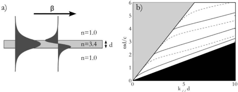
The simplest guided modes in a planar structure are waveguide modes. A waveguide can be constructed by surrounding a high refractive index dielectric by media with a lower refractive index. Light in the high refractive index ma-terial is bound to this medium by total internal reflection from the interfaces. In a planar waveguide, the waveguide modes can be classified as having the electric field pointing parallel to the waveguiding plane (TE modes) or perpen-dicular to this plane (TM modes), and by the number of zeros the field has in the waveguide (the mode number). Figure 1.2(a) sketches the electric field distribution of the two first TE waveguide modes for a planar waveguide [14]. The dispersion relation of the different waveguide modes can be calculated numerically. This is done by imposing a wave solution that is exponentially decaying outside the slab, and sinusoidal inside the slab. Boundary conditions at each interface require that the parallel components of the fields are contin-uous across the interface, which allows us to numerically find solutions for the waveguide modes.
Figure 1.2(b) shows the dispersion relation of the first waveguide modes for a slab with refractive indexnslab= 3.4, surrounded by air. Note that both the frequency and the wave vector axis of this graph are scaled by the thicknessd of the slab. This reflects the fact that Maxwell’s equations are scale invariant. Three different regions can be identified in this graph. The grey area in this graph shows the light cone. In this region, a continuum of solutions exists for a chosen parallel wave vectorkk. These solutions have a propagating component
in directions away from the slab (k⊥ is real everywhere), and are therefore not
bound to the dielectric slab.
In the black region, k⊥ is imaginary in all regions of space, and no
1.2 Bound modes in slabs and at surfaces
n=1.0 n=3.4
n=1.0 !
d
0 5 10
0 1 2 3 4 5 6
k//d
!
d/c
b) a)
Figure 1.2. (a) Electric field distribution of the first two TE waveguide modes of a slab with refractive indexn = 3.4, surrounded by air. (b) Dispersion diagram of this structure. The solid and dashed curves give the dispersion of the TE and TM waveguide modes, respectively. The grey area indicates the light cone, were propagating solutions exist that are not bound to the slab. The black area indicates the region where no propagating modes exist at all.
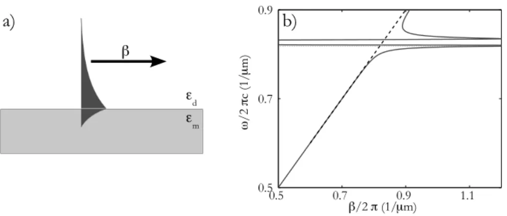
1.2.2 Surface plasmons
On a metal-dielectric interface, another kind of bound wave exists. This is the so-called surface plasmon polariton (surface plasmon for short) [15]. A surface plasmon is a collective oscillation of charges at the boundary between a metal and a dielectric. For a surface plasmon, the magnetic field points parallel to the surface, normal to the propagation vectorβ. It has a field distribution that is decaying exponentially in both the metal and the dielectric, as is shown in Fig. 1.3(a). Its dispersion relation is shown in Fig. 1.3(b) and is given by
β(ω) = ω c
s
dm(ω)
d+m(ω), (1.5)
!
"d "m
0.5 0.7 0.9 1.1
0.5 0.7 0.9
!/2" (1/!m)
#
/2
"
c (1/
!
m)
b)
a)
Figure 1.3. (a) Magnetic field distribution for a surface plasmon. (b) Dispersion relation for a surface plasmon on a gold-air interface. For low frequencies, the surface plasmon is close to the light line, indicated by the dashed line. The horizontal dotted line indicates the plasmon frequency.
1.3
Periodic guiding structures
When a planar material that contains guided modes, is patterned with a pe-riodic structure, diffraction will allow light that is incident, to couple to the guided waves, and vice-versa. This is most easily visualized by considering the dispersion relation of the guided wave, and imposing the periodicity of the lattice to the dispersion relation. Figure 1.4 shows the dispersion diagram of the first two waveguide modes from Fig. 1.2, where a one-dimensional period-icity with reciprocal lattice vectorGwas imposed by repeating the dispersion relation.
A few things can be noticed in this figure. First, by repeating the disper-sion relation every reciprocal lattice vector, the frequency ω of a particular mode with well-defined kk is not uniquely defined anymore. Moreover,
differ-ent waveguide modes cross. At the crossing of two waveguide mode lines in this diagram, interaction between the modes can induce an avoided crossing between the curves, leading to a more complicated dispersion relation. This interaction is caused by the Fourier component of the dielectric function, at the reciprocal lattice vector that links the two crossing curves.
1.3 Periodic guiding structures
G0 G/2 0 G/2 G 1
2
k//d
!
d/c
Figure 1.4. Construction of the dispersion relation of the dielectric waveguide of Fig. 1.2, that is patterned with a one-dimensional array of infinitesimal lines. The lattice perioda= 2.5d, where dis the thickness of the slab. Only the two first waveguide modes are shown. The grey area indicates the light cone. The dash-dotted lines indicate diffraction orders into the surrounding air.
layer. The condition for such a resonance to occur is given by
~kk =β~+G,~ (1.6)
where ~kk is the parallel component of the wave vector of the incident light.
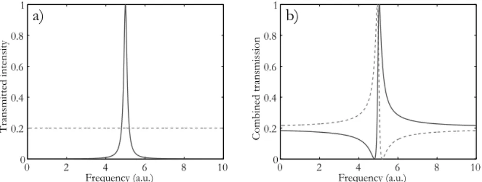
Although this equation gives the frequencies at which resonances occur, the coupling strength, and therewith the width of the resonance, is determined by the Fourier spectrum of the dielectric function.
shape as in Fig. 1.5(b). The asymmetry of the peak will be determined by the relative phase of the two channels.
0 2 4 6 8 10
0 0.2 0.4 0.6 0.8 1
Frequency (a.u.)
Combined transmission
0 2 4 6 8 10
0 0.2 0.4 0.6 0.8 1
Frequency (a.u.)
Transmitted intensity
a) b)
Figure 1.5. (a) Transmission intensity as function of frequency, for the direct (dashed line) and resonant (solid curve) transmission channel. When the two channels are combined, an asymmetric line shape arises due to the coherent addition of the two channels (b). The relative phase of the direct and resonant channel determines the asymmetry of the peak, either red-tailed (dashed curve), or blue-tailed (solid curve).
1.4
This thesis
In this thesis, we investigate how light couples to periodic nanostructures. We study different structures, and start out with dielectric structures. In chapter 2 we discuss the fabrication and reflection spectra of two-dimensional photonic-crystal slabs. We discuss the resonances in terms of a Fano model, and show that light can be coupled resonantly to waveguide modes in the slab. In chapter 3 we discuss the line shape of these resonances, and show that the line shape changes when the angle of incidence is tuned. In chapter 4 we study one of these resonances in more detail. For this, we change to a direct-imaging scheme, which allows us to show the propagation of the light through the resonant modes.
1.5 Polarization convention
surface plasmon modes, this dielectric layer acts as a waveguide, which gives rise to extra resonances in the transmission spectra. Finally, in chapter 7, we study surface plasmon modes on both sides of the hole array, that are made degenerate by immersing it in an index-matching liquid, and discuss the coupling that is a result of this degeneracy.
The last two chapters discuss the optics of a new kind of single-photon detector, that consists of a very thin superconducting meander. We study the polarization dependence of these detectors in chapter 8, and we describe the absorption of light in this thin meander in terms of an optical impedance model. In chapter 9, we show that the absorption in a metallic film of only a few nanometers thickness can be as high as 95%, for one single polarization. Besides that, we extend these results to the geometry of the single-photon detectors, and show that it is equally possible to make a detector with such a high absorption efficiency.
1.5
Polarization convention
Throughout this thesis, I tried to consistently use the following classifications for the polarization of light in experimental setups and for the polarization of different modes. When a mirror symmetry is present, modes will have a profile that is either even or odd with respect to this symmetry plane. The polarization is also defined with respect to these symmetry planes:
• s- and p-polarization define a polarization with respect to the scatter-ing plane of a reflection. Light that has its electric field perpendicular (senkrecht) to this plane (i.e., parallel to the reflecting surface) is denoted with s-polarization, whereas light that has the electric field parallel to the scattering plane, is denoted as being p-polarized.
Part I
Chapter 2
Fano resonances and waveguide
modes in a two-dimensional
photonic-crystal slab
The measured reflection spectra of two-dimensional photonic crys-tal slabs consist of an asymmetric peak on top of an oscillating background. For p-polarized light, this asymmetric peak changes shape, when the angle of incidence is tuned over Brewster’s an-gle. We explain the observed line shapes with a Fano model that includes loss and use a waveguide model to predict the resonance frequencies of the photonic-crystal slab. Finite-difference time do-main calculations support the model and show that resonances due to higher order waveguide modes disappear when the substrate refractive index is increased beyond ns = 2.04. This is readily explained by the cut-off condition of these modes, given by the waveguide model.
This chapter is based on E. F. C. Driessen, P. O. M. Heemskerk, D. Stolwijk, E. W. J. M.
van der Drift, and M. J. A. de Dood, Asymmetry reversal and waveguide modes in the
2.1
Introduction
Resonant optical structures, in particular photonic crystals embedded in a waveguide, form an important class of optical materials. These photonic-crystal slabs contain a periodic arrangement of holes on a wavelength scale, and allow control of the propagation of light, guided in the plane of the waveg-uide [16]. For example, they enable wavelength-dependent steering [17], strong coupling of atoms to a cavity [18], and enhanced non-linear optical effects [8]. A measurement of the reflectivity as a function of the wavelength is a relatively easy way to characterize the optical properties of these slabs. At each angle of incidence, the reflectivity spectrum shows a number of reso-nant features related to coupling of incident radiation to a leaky waveguide mode of the photonic-crystal slab [19, 20]. The reflection spectra can be calcu-lated numerically by solving Maxwell’s equations using a scattering-matrix ap-proach [21,22], Green’s functions [23], or finite-difference time domain (FDTD) methods [19, 24]. Although these numerical solutions of Maxwell’s equations predict the right frequencies and quality factors of the resonances observed in the measurements, they do not give physical insight into the origin of the spec-tral features. Therefore, it is important to develop simpler models to explain the measured resonances. Such models can be used as a diagnostic tool for fabricated structures, and can facilitate the first design of a photonic crystal structure.
Here, we present reflection measurements on a two-dimensional (2-D) photonic-crystal slab. We use an extended coupled-mode theory to describe the shape of the measured reflectivity spectra and the line shape of the resonant features. This theory explains the change in asymmetry that is observed when chang-ing the angle of incidence, as resultchang-ing from the change of sign of the Fresnel reflection coefficient of the layered structure at Brewster’s angle. We use a waveguide model [25, 26] to predict the resonance frequencies of a photonic-crystal slab and compare this model to FDTD calculations. The disappearance of modes from the spectra when increasing the refractive index of the substrate is explained by the model in terms of the cut-off condition of the guided modes.
2.2
Photonic crystal fabrication
The GaAs and AlGaAs photonic crystals in this study were fabricated using a combination of electron-beam lithography and reactive ion etching∗. A square lattice of1000×1000holes, with a radiusr≈100nm and a lattice constanta≈
∗
2.2 Photonic crystal fabrication
Figure 2.1. SEM images of photonic crystal structures fabricated by reactive ion etching in a Cl2/N2 plasma. (a) Top view of the photonic
crystal structure used for the measurements in Sec. 2.4. The arrow corresponds to the direction of kk in the reflection measurements. (b)
Cross section (taken under an angle of 45◦) of the etched holes when no N2is added. The non-passivated side walls are partially etched away by
the plasma. (c) Cross section of the holes (taken under an angle of 55◦) when 10 sccm of N2 is added to passivate the side walls. The silicon
nitride mask on top is still visible.
320nm, was defined by electron-beam lithography in a ∼550nm thick layer of ZEP 520 positive-tone resist∗ on top of a∼300nm layer of silicon nitride. After development, the pattern was transferred to the nitride by reactive ion etching using a low pressure (<8µbar) CHF3:Ar (1:1) plasma. The remaining ZEP resist was removed with an oxygen plasma.
The resulting hole pattern in the nitride serves as a mask for reactive ion etching of the (Al)GaAs with a chlorine-based plasma [5, 27]. In this process, the chlorine ions etch the (Al)GaAs, while the nitrogen is used to passivate the side walls. We used a power of 100 W, a pressure<5 µbar, and a flow of 15 sccm BCl3and 7.5 sccm Cl2, and varied the N2flow to tune the profile of the side walls. The selectivity of the etching process is>10 : 1, and the etch rate depends on the hole size and the nitrogen flow, i.e. ∼ 200 nm/min for holes with a diameter of 300 nm, and∼1µm/min for holes with a diameter of 1µm, with N2 added. Figure 2.1(a) shows a scanning electron microscope (SEM) image of the photonic crystal after the fabrication process. Figure 2.1(b) shows a cross section of the holes when using a plasma without N2 added, showing damage to the side walls of the holes. In Fig. 2.1(c), we added a flow of 10 sccm N2 to the plasma, resulting in straight holes. A slight curvature of the holes is observed in Fig. 2.1(c). The curvature is due to specular reflection of the ions from the slightly tapered nitride mask, and the depth at which it occurs depends on the hole diameter. This curvature is therefore not intrinsic to the
∗
Figure 2.2. SEM images of (a) the cross section of the photonic crystal used for the measurements in section 2.4 (taken under an angle of 59◦). The approximate shape of the holes is indicated with the white curves. (b) A large, high-quality, free-standing photonic-crystal membrane. The GaAs capping layer is not removed from the membranes in this picture. The inset shows an enlarged image of the holes. The length of the scale bar in the inset is 500 nm.
process and straight holes as deep as a few microns can easily be achieved. In the final stage, we selectively removed the silicon nitride mask using the same CHF3:Ar reactive ion etch used to define the mask.
Figure 2.2 shows SEM images of photonic crystal samples that consist of a higher refractive index slab layer on top of a substrate with a lower index. The structure in Fig. 2.2(a) was fabricated in a GaAs substrate using a relatively low N2 flow, leading to incomplete passivation of the side walls. The lines in the figure indicate the resulting tapering of the holes. The undercut effectively defines a waveguide structure that was used in the optical measurements of Sec. 2.4.
2.3 Theory
2.3
Theory
The reflection spectrum of a photonic-crystal slab typically consists of an os-cillating background and a number of sharp resonances [19, 20] as shown in Fig. 2.4 and Fig. 2.6. The spectrum can be explained using a simple scattering model of a resonator coupled to a continuum of modes. The photonic-crystal slab, that acts as the resonator, is depicted in Fig. 2.3(a), together with the input and output ports. Part of the radiation incident on the slab is diffracted into a leaky waveguide mode (dashed arrows), whereas another part is directly reflected and transmitted (solid arrows). The radiation that is diffracted back from the waveguide mode interferes with the directly reflected and transmit-ted radiation, yielding the characteristic Fano line shape [29]. In Sec. 2.3.1 we extend a temporal coupled-mode theory [30] to include loss, and describe the reflection in terms of the parameters of the direct and resonant channels. After that, in Sec. 2.3.2, we introduce a waveguide model to predict the resonance frequency of the resonant channel.
2.3.1 Fano model
To calculate the spectrum of the transmitted and reflected light, we proceed as follows. For each angle of incidence and each wavelength, a scattering matrix links the amplitudes of the incident, reflected, and transmitted waves. The scattering matrixS of the system is the sum of the scattering matrices of the direct and the resonant channel. The direct channel is described by a scattering matrix C, given by
C =
r1 t21 t12 r2
· · ·
..
. . ..
, (2.1)
that connects the amplitudes of the modes (ports) on both sides of the slab. When there are no propagating diffraction orders in the media above and be-low the guiding layer, the components of the scattering matrix are given by the Fresnel reflection and transmission coefficients for a homogeneous layered sys-tem. The contribution from the direct channel gives rise to typical oscillations in the reflectivity as a function of wavelength (Fabry-Perot fringes). If there are propagating diffraction orders in the media above or below the guiding layer, a more elaborate method is needed to calculate the matrix elements of C.
Figure 2.3. (a) Schematic drawing of the direct and resonant reflection and transmission in a photonic-crystal slab. The incident light in port 1 can be scattered via the direct channel (solid arrows) or diffracted into a waveguide mode (resonant channel, dashed line). The waveguide losses can be modeled by including a third port (dotted arrow) to the system. (b) Geometry of the photonic-crystal slab used in the FDTD calculations in section 2.3.2. The slab of thicknessdand refractive indexng contains
a periodic array of air slits with a widthwand a periodicitya. The slab is supported by a substrate with refractive indexns, and covered by air
(n0= 1) on the top.
crystal structure. For a fixed angle of incidence, the coupling to a specific waveguide modep occurs at a resonance frequencyωp and is characterized by
an escape rate γp. This escape rate parametrizes the life time of light in the
waveguide mode. The coupling to the waveguide mode is described by coupling constants dj,p, where the index j corresponds to the different ports coupling
to the waveguide mode. The coefficients γp, dj,p, and the matrix elements
Cjk are not independent. Time-reversal symmetry and energy conservation
put the following constraints on the coupling constants (a derivation of these conditions is given in Ref. 30):
X
j
|dj,p|2 = 2γp, (2.2)
X
k
Cjkd∗k,p = −dj,p, (2.3)
where the indicesjandkrefer to the different ports, andCjk are the elements
of the direct transmission matrix connecting the different free-space modes. Equation (2.3) links the amplitude and phase of the coupling constants to the scattering matrixC of the direct process.
2.3 Theory
of direct and indirect coupling are given by
Sjk =Cjk+ X
p
dj,pdk,p
i(ω−ωp) +γp
, (2.4)
where ω is the angular frequency of the incident radiation. The reflection coefficients for the different ports are given by the diagonal elements of this matrix, and the transmission coefficients by the off-diagonal elements. This description which uses a Lorentzian line shape for the resonant channel, is a simplification which holds as long as ωpΓp+γp. The small frequency shift
that results from describing our resonance with a Lorentzian can be included in the resonance frequencies ωp. It is important to stress that the equations
derived here hold for the case of uncoupled waveguide modes only. For the modes to be uncoupled, it is necessary that the number of independent ports, i.e. the rank of the matrix Cij, is larger than or equal to the number of
waveguide modesp [31].
Losses can be included in the description in this model, by discriminating between losses in the direct channel, due to absorption or surface roughness, and losses in the resonant channel. Losses in the resonant channel can also be due to scattering of the waveguide mode to ports that are not incorporated in the scattering matrix description.
Absorption losses in the direct scattering channel can be adequately de-scribed by using a non-unitary scattering matrixCand the Fresnel coefficients of a layered system with complex-valued refractive index. This matrix can be made unitary by adding an extra port to the description. If we assume that the input in this extra port is zero, and that the loss port is not coupled to the resonator mode, then the scattering matrixS includes a block matrix describ-ing the normal input and output ports of the system, that is not influenced by the parameters of the loss port. This makes it possible to use Eqs. (2.2)-(2.4), while using a non-unitary scattering matrix C for the direct channel.
Waveguide losses can be incorporated in a similar way, by extending the model with extra loss ports, which only couple to the specific waveguide modes. Each waveguide mode couples to its loss port with a coupling constantΓp. The
direct scattering matrix for a two-port system with an additional loss port acquires the form
C =
r1 t21 0 t12 r2 0
0 0 1
. (2.5)
The loss rates Γp are incorporated in Eq. (2.2) in a straightforward way, by
using the conventionP
all ports.
For the symmetric case of two ports coupled to only one leaky waveguide mode, symmetry requires that r1 = r2 = r and t21 = t12 = it, where r and t are real. Moreover, the coupling constants to the ports should be equal, except for a plus or minus sign determined by the odd or even symmetry of the waveguide mode with respect to the mirror plane. The reflectivity in this case is given by
R=
r+γ −r∓it i(ω−ω0) +γ+ Γ
2
, (2.6)
where the∓is determined by the even or odd symmetry of the mode [30], and the parametersω,γ, andΓlost their subscripts since we are dealing with only one waveguide mode. This expression gives the typical asymmetric Fano line shape. The reflectivity has a distinct zero if the loss rateΓ = 0. To reach 100% reflectivity, the direct process has to be lossless as well (i.e. |r|2+|t|2 = 1).
2.3.2 Waveguide modes
The model in the previous section gives a description of the line shape in the reflectivity of a photonic-crystal slab, but it does not predict the resonance frequencies ωp. As we will show in this section, it is possible to calculate
the resonance frequencies and the waveguide modes for a photonic-crystal slab using a simple model [25,26,32]. In this nearly-free photon approximation, the waveguide is treated as a uniform slab with an effective refractive index that depends on the filling factor of the air holes. For the TE waveguide modes, having the electric field in the plane of the slab, the dispersion relation for a uniform slab is implicitly defined as [14]
sin(hd) h2−pq= cos(hd)(p+q)h, (2.7) wherep,q, and hdenote the transverse components of the wave vector in the different media. They are defined asq2 =β2− ω2/c2n20,h2= ω2/c2n2g−β2, and p2 = β2− ω2/c2n2s, where n0, ng, and ns are the refractive indices of the top, guiding, and bottom layer, respectively, and c is the speed of light in vacuo. The condition for coupling to a waveguide mode is given by the diffraction condition
~kk+G~ =β,~ (2.8)
where~kkis the parallel component of the incident wave vector,β~is the parallel
2.3 Theory
~
β = G, which can be used to numerically find the resonance frequencies~ ωm
from Eq. (2.7).
0.2 0.4 0.6
0.0 0.5 1.0
Refle
ctivity
ns=1.0
0.2 0.4 0.6
ns=2.0
0.2 0.4 0.6
ns=2.3
0.2 0.4 0.6
ns=2.5
Frequency!(2"c /a)
Figure 2.4. Reflectivity of a 1-D photonic-crystal slab, calculated using a FDTD method. The grating consists of air slits withw/a= 0.1 in a dielectric slab with d/a= 0.5 and refractive index ng = 3.5, on top of
a substrate with increasing refractive index. Two resonances are visible, on top of an oscillating background. The dashed curve is a fit to the background of a refractive index of the form described in Eq. (2.9). The resonance aroundω= 0.5disappears forns>2.0.
For simplicity, we calculated the reflectivity of an one-dimensional (1-D) array of slits, using a freely available FDTD package [33]. The cross section of the structure used in these calculations is given in Fig. 2.3(b). The slab of thickness d and refractive index ng = 3.5 contains an array of slits of width w and refractive index n0 = 1. The array has a lattice constant a and we used w/a = 0.1 and d/a = 0.5. The substrate index ns was varied between 1 and 3.0, and the reflection spectra were calculated at normal incidence for TE-polarized light (E-field parallel to the slits).
Figure 2.4 shows the reflectivity of the array as a function of frequency, for increasing substrate index ns. Two distinct resonances are visible on top of an oscillating background. The Fresnel reflection coefficient for the layered system can be fitted to the spectra, using an effective refractive index of the form [24]
0.2 0.4 0.6 0.0
0.5 1.0
Frequency ! (2" c / a)
Reflectivity
a) b)
1.0 1.5 2.0 2.5 3.0 Substrate index ns 0.30 0.35 0.40 0.45 0.50 0.55 0.60 F re q u e n c y !0 (2 " c/a )
1.0 1.5 2.0 2.5 3.0 Substrate index ns 0.30 0.35 0.40 0.45 0.50 0.55 0.60 F re q u e n c y !0 (2 " c/a )
Figure 2.5. (a) Calculated reflectivity of the array of slits at 5◦ angle of incidence, for a substrate indexns= 1. Two resonances that are not
visible at normal incidence appear atω≈0.33and ω≈0.48. (b) Reso-nance frequencies of the Fano resoReso-nances as a function of the substrate refractive indexns. The resonance frequencies can be predicted using a
simple waveguide model (red curves), withng given by effective medium
theory. This model does not include the avoided crossing between the two waveguide modes, and therefore calculates the average of the high-frequency and low-high-frequency resonances. The dashed curves correspond to the cut-off conditions of them= 0andm= 1modes. The gray area indicates the parameter region where higher order diffraction into the substrate occurs.
2.3 Theory
a rigorous coupled wave analysis [37]. In this figure, the lower-frequency reso-nances can be seen to appear as narrow resoreso-nances atω= 0.33 and ω= 0.48. As can be seen in Fig. 2.4, the two resonances visible for ns ≤2.0 at nor-mal incidence have opposite symmetry. This is consistent with the fact that these resonances are due to the first and second TE waveguide mode, that have an even and odd field distribution, respectively. For a refractive index ns > 2.0, the second resonance is seen to disappear from the spectrum. We fitted Eq. (2.6) to the calculated spectra, using the refractive index obtained by the fit of the oscillating background as an input. The only fit parame-ters are the resonance frequencies ω0 and ω1, and the line widths γ0 and γ1. The resulting resonance frequencies are shown as the symbols in Fig. 2.5(b), plotted as a function of the substrate refractive index, and are compared to the numerical solution of Eq. (2.7) (solid curves) obtained using ng = 3.34. The calculated frequencies are below the frequencies obtained from the fits, because the waveguide model predicts the center frequency and does not take into account the avoided crossing. In fact, the data in Fig. 2.5(a) for 5◦ an-gle of incidence show that the waveguide model correctly predicts this center frequency.
The disappearance of the resonance is also predicted by the waveguide model. The cut-off frequency of them-th mode is given by [14]
ωcm=
c 2πdqn2
g−n2s
mπ+ arctan s
n2 s−n20 n2
g−n2s !
. (2.10)
This condition is drawn with dashed curves in Fig. 2.5(b) for the first two waveguide modes, calculated using an effective refractive index ng = 3.34. Diffraction into the substrate occurs at a frequencyωd, where the propagation constant β becomes equal to the length of the wave vector in the substrate. This leads to the condition
ωd= (kk+G)/ns. (2.11)
The existence of diffraction orders at normal incidence is indicated by the grey area in Fig. 2.5(b). This corresponds to the situation where the transverse component of the wave vector in the substratep= 0. The resonance frequency of the waveguide modeat cut-off is thus given by the intersection of Eq. (2.10) and Eq. (2.11).
modes to appear in the TM spectra, and vice-versa. This makes identification of specific peaks with specific waveguide modes more complicated.
2.4
Reflection measurements
We measured the specular reflection from the GaAs photonic-crystal slab shown in Fig. 2.1(a) along the Γ-X direction (indicated with the arrow) as a function of the angle of incidence from 25◦ to 80◦. White light from a spec-trally broad lamp was polarized and focused onto the sample. The specular reflection was polarization-filtered, imaged onto a fiber, and analyzed in a spec-trometer with a spectral resolution of ∼2 nm. The numerical aperture (NA) of the incoming beam was limited toNA<0.04. The spot size on the sample was∼100µm.
0.6 0.8 1.0 1.2 1.4 1.6 0.6 0.8 1.0 1.2 1.4 1.6 0.6 0.8 1.0 1.2 1.4 1.6
0.0 0.2 0.4 0.0 0.2 0.4
s - polarized p - polarized crossed polarizers
50
o
80
o
a) b) c)
d) e) f)
x 0.5 x 100
x 10
Wavelength (µm)
Re
fle
ct
ivit
y
Figure 2.6. Experimental reflection spectra of a photonic-crystal slab for two angles of incidence, 50◦ [(a) to (c)] and 80◦ [(d) to (f)], for
s-polarized [(a) and (d)] and p-polarized light [(b) and (e)], and for a crossed polarizer setup, where the incoming light was p-polarized and the detected light was s-polarized [(c) and (f)]. The dashed curves are fits using the model discussed in the text. Figures (c), (d), and (f) are scaled with the factors indicated, to enhance visibility.
2.4 Reflection measurements
peak around a wavelength of ∼950nm is seen on top of an oscillating back-ground. The peak position changes with angle of incidence. Similar peaks can be seen in Fig. 2.6(b) and (e), where both polarizers were set to a polarization parallel to the scattering plane (p-polarization). In this case, the asymmetry of the peak is changed when tuning the angle of incidence from 50◦ to 80◦ The symmetry of the peak is the same for both polarizations at 80◦ angle of incidence.
The Fano model described in Sec. 2.3.1 can be used to describe the obser-vations. We use Maxwell-Garnett’s effective medium theory [34,35] to describe the photonic crystal layer as a homogeneous birefringent layer with an effec-tive refraceffec-tive index neff, incorporating the known refractive index dispersion of GaAs [39]. This includes absorption for wavelengths shorter than 950 nm. With this effective index, we calculate the polarization- and angle-dependent Fresnel reflection and transmission coefficients of the layered system.
The dashed curves in Fig. 2.6 show fits of the Fano model to the measure-ments. The only fit parameters were the resonance frequencyω0, the linewidth γ, and the waveguide lossesΓ. We slightly adjusted the effective index neff for different angles of incidence, to get a better fit to the oscillating background. Although the fits deviate on detail from the measurements, qualitatively all elements of the measurement are contained in the model. We attribute most deviations to the simplifications we made with respect to the vertical shape of the air holes, and to the fact that effective medium theories only hold when all relevant length scales in the system are much smaller than the wavelength. In fact, the tapering of the holes is essential to observe the resonances. It en-sures that there is a waveguiding layer in the top part of the photonic-crystal structure, that provides a discrete mode.
The Fano model also gives a direct explanation for the change in asymmetry of the peak. Since the peak shape is determined by interference of a resonant and a direct channel, the relative phase between these two contributions de-termines the asymmetry of the resulting peak. The Fresnel coefficient r for s-polarized light is always negative, but the Fresnel coefficient for p-polarized light vanishes and changes sign at Brewster’s angle. It is exactly this change of sign that causes the line shape to change when the angle of incidence is tuned to larger angles (see Ch. 3 and Refs. 40, 41). The fact that the asymmetry for s-polarized light is the same as forp-polarized light at large angles of incidence indicates that both peaks are due to coupling to a waveguide mode that is even in the center plane of the photonic-crystal slab.
light was s-polarized. A small Lorentzian-shaped peak can be observed in these spectra. The resonance frequencies obtained from the fits of the different measurements are not exactly identical for the same angle of incidence. This indicates that the peaks in Fig. 2.6(a), (b), and (c) are due to different waveg-uide modes. Since Fresnel reflection is polarization-maintaining for s- and p-polarization, the direct channel is filtered out by the second polarizer. This results in a resonant contribution only, explaining the Lorentzian line shape of the peak [42]. The intensity of these peaks is low, because the symmetry of the photonic-crystal lattice dictates that the polarization (sorp) is conserved upon transmission and reflection, as long as the wave vector kk is along one
of the symmetry directions of the lattice. The fact that we do observe a small peak demonstrates that our structure does not have perfect square symmetry.
2.5
Conclusion
In summary, the typical asymmetric peaks on top of an oscillating background, observed in the reflection from a photonic-crystal slab, are due to interference between a direct and a resonant reflection channel. The observed change of asymmetry of the peak, for p-polarized light, is caused by a change of sign of the direct reflection at Brewster’s angle. This asymmetry change will be discussed in detail in Ch. 3. The rough shape of the holes in our experiment causes relatively broad spectral features that are easily resolved. The fact that we are able to describe our data with a coupled mode theory and observe the change in asymmetry of the spectral line shows that the description is robust and also valid for less-than-perfect photonic crystals.
Chapter 3
Asymmetry reversal in the reflection
from a two-dimensional
photonic-crystal slab
The measured, angle-dependent, reflection spectra of a 2-D GaAs photonic-crystal slab consist of an asymmetric peak on top of an oscillating background. At large angles of incidence (> 70◦), the asymmetry of the peak is observed to flip for p-polarized light. We explain the observed spectra with a Fano model that includes loss and interference between a resonant waveguide component and direct Fresnel reflection of the layered structure. We show that the reversal of the asymmetry of the line is due to a change in sign of the direct reflection at Brewster’s angle.
This chapter is based on E. F. C. Driessen, D. Stolwijk, and M. J. A. de Dood,
3.1
Introduction
Optical reflectivity measurements of two-dimensional photonic-crystal slabs are a relatively easy way to characterize the properties of these slabs. The wavelength dependent spectra show a number of features related to the leaky waveguide modes of the slab [19, 20]. A lot of effort has been devoted to calcu-lating these spectra by rigorously solving Maxwell’s equations, using scattering matrices [21,22], Green’s functions [23] and finite difference time domain meth-ods [19, 24]. Although being able to reproduce the spectra, these calculations do not give physical insight into the origin of the spectral features. Therefore it is important to develop simpler models that can explain the measured reso-nances. Such models are an important diagnostic tool for fabricated structures and can facilitate the first design of a photonic crystal structure.
In this Chapter, we present reflection measurements on a 2-D photonic-crystal slab. We study the line shape of a resonance in this spectrum, as a func-tion of the angle of incidence. The asymmetry of the (Fano) line shape [29, 30] in the reflection spectra is observed to change forp-polarized light. Our obser-vations can be described with an extended coupled mode theory, linking the reversal of asymmetry to the change of sign of the Fresnel reflection coefficient of the layered structure. This change of sign occurs at Brewster’s angle.
3.2
Experiment
The photonic crystal in this study was fabricated in GaAs using e-beam lithog-raphy and reactive ion etching. It consists of a square lattice of 1000×1000 holes with radiusr ≈100nm and lattice constant a≈320nm. Figure 2.1(a) shows a scanning electron microscope (SEM) image from the top, and Fig. 2.2(a) a cross-section (made with a focussed ion beam). Due to details of the fab-rication process, the cross-section of the holes consists of two slightly tapered parts, as can be seen in figure 2.2(b). The holes become wider until a depth of
∼600nm, and then narrow down until a depth of 1.5−2µm.
We measured the specular reflection from the photonic crystal along the Γ-X direction [indicated with the arrow in figure 2.1(a)], as a function of the angle of incidence from 25◦to 80◦ in steps of 2.5◦. White light from a spectrally broad lamp was polarized and focused onto the sample. The specular reflection was polarization-filtered, imaged onto a fiber and analyzed in a spectrometer with a spectral resolution of ∼ 2 nm. The numerical aperture (NA) of the incoming beam was limited to NA <0.04. The spot size on the sample was
3.3 Model
results for p-polarized light.
Reflection spectra for angles of incidence of 50, 70 and 80◦ are shown in figure 3.1. The spectra show a large, asymmetric peak, on top of an oscillating background. By changing the angle of incidence, the peak shape in figure 3.1 changes from asymmetric with a tail on the red side (a), to symmetric (b), to asymmetric with a tail on the blue side (c).
600 800 1000 1200 1400 1600 0 10 20 30 40 50 60 70 Wavelength (nm) R e fl e c ti o n (% ) (c)
0 20 40 60 80
-1 -0.5 0 0.5 1 Angle (o)
r 10
.5
-.5
-1
0 20 40 60 80 r1
Angle ( )o
600 800 1000 1200 1400 1600 0 10 20 30 40 50 60 70 Wavelength (nm) R e fl e c ti o n (% ) (b)
0 20 40 60 80
-1 -0.5 0 0.5 1 Angle (o)
r 10
.5
-.5
-1
0 20 40 60 80 r1
Angle ( )o
600 800 1000 1200 1400 1600 0 10 20 30 40 50 60 70 Wavelength (nm) R e fl e c ti o n (% ) (a)
0 20 40 60 80
-1 -0.5 0 0.5 1 Angle (o)
r 10
.5
-.5
-1
0 20 40 60 80 r1
Angle ( )o
Figure 3.1. Experimental reflection spectra of the photonic-crystal slab for 3 angles of incidence: 50◦ (a), 70◦(b) and 80◦ (c). The dashed lines
are fits using the model discussed in the text. The insets show the reflection coefficientr1for an interface of air andneff = 2.5, as function
of angle of incidence. The circles indicate the angle of the measurement.
3.3
Model
In order to explain our measurements, we extended the temporal coupled-mode theory in Ref. 30, by including an additional loss port. Light incident onto the photonic-crystal slab can be reflected through different channels: a non-resonant (direct), and a resonant loss channel. The direct channel cor-responds to the Fresnel reflection of the layered system, while the resonant channel is created by coupling to a (leaky) waveguide mode. This waveguide mode has a well-defined dispersion relation and coupling at a specific frequency occurs via diffraction. The asymmetric Fano line shape can be explained by interference between the direct channel and the resonant channel. A loss port is added to include the effects of scattering from surface roughness and diffrac-tion into the substrate. All input and output ports of the system are linked by a direct-scattering matrixC and a resonant scattering matrixU. Coupling of the resonant mode to the three different ports is described by the complex coefficientsdj.
the layered system. At each angle of incidence, we use Maxwell-Garnett’s effective-medium theory [34, 35] to describe the photonic crystal layer as a birefringent layer with refractive index neff. We then calculate the Fresnel reflection and transmission coefficients [43] of the layered system shown in figure 3.2(a), incorporating the known refractive-index dispersion of GaAs [39], that includes absorption for wavelengths shorter than 950 nm. Taking the loss port into account, we write the scattering matrix for the direct process as
C =
r1 t 0 t r2 0
0 0 1
, (3.1)
wherer1,r2 and tare the (complex) Fresnel reflection and transmission coef-ficients for the electric field.
The resonant channel, due to the leaky waveguide, is formed by the pho-tonic crystal layer. As pictured in figure 3.2(b), the incident light is partially diffracted into the waveguide and confined by internal reflection. The light that is diffracted back, interferes with the directly reflected and transmitted light (ports 1 and 2 in figure 3.2). The resonance angular frequency ω0 is determined by the dispersion relation of the waveguide mode involved. The average lifetime in the waveguide is parameterized by an escape rate γ and is a function of angle of incidence. The scattering matrix describing the resonant channel is given by
Ujk =
djdk
i(ω−ω0) +γ
. (3.2)
whereω is the angular frequency of the incident light.
3.3 Model n=1 n=nGaAs n=neff a) b) port 1
port 2 port 3(loss)
port 1
port 2
Non-resonant Resonant
Figure 3.2. Model for the non-resonant (a) and resonant (b) channels in the model. The numbers indicate the different ports in the scattering matrix model. (a) The non-resonant channel is modeled by applying effective medium theory to the photonic-crystal layer and calculating the Fresnel reflection and transmission coefficients of the layered system. (b) For the resonant channel, the incident light is diffracted into a waveguide mode, which can diffract back to ports 1 and 2, but can also propagate into the substrate (port 3) constituting loss.
Time-reversal symmetry and energy conservation put the following con-straints on the coupling constantsdj [30]
X
k
Cjkd∗k = −dj (3.3)
X
j
|dj|2 = 2(γ+ Γ), (3.4)
whereΓ is the loss rate from the resonant mode. Furthermore, the diffractive coupling to the resonant mode is assumed to be equally large on both sides of the photonic crystal slab (i.e. |d1|=|d2|). With these constraints, we can write the coupling constants dj in terms of the Fresnel coefficients and the
parameters ω0, γ and Γ. The reflectivity R = |U11+C11|2 for the system is then given by
R =
i[(ω−ω0)r1∓γt] + Γr1 i(ω−ω0) +γ+ Γ
2 . (3.5)
After setting the fill fraction and the thickness of the photonic crystal slab once, the Fresnel coefficients are fixed and there are only three free parameters left in the model: the resonance angular frequencyω0, and the loss ratesγ and Γ.
the vertical shape of the air holes. Also, Maxwell-Garnett effective medium theory is only valid when all relevant length scales in the system are much smaller than the wavelength. This condition is not fulfilled in our structure.
Using the model described here, one can understand the origin of the change in asymmetry of peak shape when changing the angle of incidence. Since the peak is a product of interference between a resonant Lorentzian line and a non-resonant direct contribution, the relative phase between these two contri-butions will determine the asymmetry of the resulting line shape.
The Fresnel reflection coefficient (r1) for p-polarized light, for a dielectric interface, vanishes and changes sign at Brewster’s angle. This is shown in the insets of figure 3.1, for an interface between air and a dielectric withneff = 2.5. It is exactly this change of sign that causes the line shape to vary from red-tailed asymmetric to Lorentzian at Brewster’s angle to blue-red-tailed asymmetric for larger angles. Fors-polarized light, we observed the line shape to be blue-tailed asymmetric for all angles of incidence, which confirms this explanation since the Fresnel reflection coefficient for s-polarized light is always negative.
The rough shape of the holes causes relatively broad spectral features that are easily resolved. The fact that we are able to describe our data with an extended version of a coupled mode theory and observe a change in asymmetry of the spectral line shows that the description is robust and also valid for less-than-perfect crystals.
3.4
Conclusion
In summary, the reflection spectra from a 2-D photonic-crystal slab show a large asymmetric peak on top of an oscillating background. With increasing angle of incidence, the asymmetry of the peak reverses. We explained all obser-vations with a scattering matrix model [30] that is extended to include losses. The reversal of the asymmetry is a consequence of the change in sign of the Fresnel reflection coefficient when crossing Brewster’s angle. The ‘model gives good qualitative as well as quantitative agreement with the measurements, while having only three fit parameters describing the resonance frequency and lifetime of the resonant waveguide mode, and its losses.
Chapter 4
Imaging of a Fano resonance in a
two-dimensional photonic-crystal slab
4.1
Introduction
Reflection spectra from waveguides that are patterned with a periodic array of holes, so-called photonic-crystal slabs, contain a multitude of sharp, resonant features. These features are caused by diffraction from the periodic array of holes into a (leaky) waveguide mode. Light that is coupled into these leaky modes diffracts back, and interferes with the direct (Fresnel) reflection from the layered structure. This interference leads to the typical asymmetric (Fano) line shape as described in the previous chapters. Usually, information about the dispersion of these resonances is only obtained by measuring spectra at different angles of incidence [20]. These spectra are compared to calculations, and information about the resonance is distilled, most notably the specific waveguide mode that the light is coupled into. This method has the obvious disadvantage that it only works well for structures of which the constitution is reasonably well known, but even then, complications arise, since TE waveguide modes can show up in p-polarized reflection spectra, and vice-versa [46].
In this chapter, we use a different approach to obtaining information about a specific resonance of a photonic-crystal slab. We use a strongly focused, monochromatic beam to illuminate the photonic crystal at a specific spot. We image the reflection of the sample both in real space and in k-space. From the k-space images, we were able to unambiguously identify the resonance as a first-order diffraction process into the TM0 waveguide mode. Real-space images allow us to separate the resonant and non-resonant contributions of the Fano resonance. In these images, we can measure the decay length of the resonant contribution directly. From this length and the decay time, obtained from a separate measurement of the reflection spectrum, we can determine the group refractive index of the leaky waveguide mode.
4.2
Sample
4.3 Normal-incidence reflection spectrum
6000 700 800 900 1000
5 10 15 20 25
Wavelength (nm)
Reflection (%)
Figure 4.1. Normal-incidence reflection spectrum of the photonic-crystal membrane (solid curve). Two asymmetric Fano resonances are visible, centered around wavelengths of 725 nm and 882 nm. The dashed curve is a fit of a Fano model with two resonances to the measurements, as discussed in the text.
4.3
Normal-incidence reflection spectrum
The photonic-crystal slab two distinct resonances in the near-infrared spectral region. Figure 4.1 shows the reflectivity of the membrane at normal incidence, as a function of the wavelength of the incident light. To record this curve, we used an unpolarized, fiber-coupled xenon lamp and imaged the 50 µm -diameter fiber facet onto the sample, while limiting the numerical aperture of the incident light to <0.01. The reflected light was collected with a 200µm core-size fiber and sent to a grating spectrometer∗, to analyze the spectral content. The detected signal was normalized to the reflection from a silver mirror.
The measurement in Fig. 4.1 shows two asymmetric (Fano) resonances, centered around wavelengths of 725 nm and 882 nm. We ascribe the small peak that is observed around 670 nm to luminescence at the band edge of
∗
the AlGaAs material, and not to a resonance that is caused by the patterning of the membrane. This assumption is confirmed by the fact that the peak does not change spectral position when changing the angle of incidence of the illumination. To obtain a better understanding of the reflection spectrum, we used the Fano model described in Ch. 2. In this model, the reflection is given by R=
r−X
p
γp
r±it i(ω−ωp) +γp+ Γp
2 , (4.1)
whererandtare the reflection and transmission coefficients of the direct con-tribution, respectively,ωis the angular frequency of the light,ωpthe resonance
angular frequency,γpthe radiative loss, andΓpthe irreversible (scattering) loss
of waveguide modep. In order to fit this model to the measurements, we as-sumed that the reflectionris constant over the wavelength range. Furthermore, we assumed that the transmission t is given by|t|2 = 1− |r|2, i.e. that there are no losses in the direct channel. We checked this assumption by adding some loss in the direct channel (i.e., |r|2+|t|2 <1). This addition of loss did not change the overall quality factor Q=ωp/(γp+ Γp) of the resonances
sig-nificantly. It does change the relative contributions of γp and Γp in Eq. (4.1),
which makes a reliable independent fit of these two parameters impossible. The buckling of the membrane structure causes a variable distance between the free-standing membrane and the GaAs substrate. This results in an am-biguity of both the precise angle of incidence and the vertical structure of the different layers. Combined, this makes it impossible to calculate the Fresnel coefficients for direct reflection and transmission for this structure, contrary to the structure discussed in chapters 2 and 3.
4.4 Imaging of the resonance
Table 4.1. Fit parameters and 95% confidence intervals of the two-resonance Fano model.
Parameter Value
Resonance 1 Resonance 2
r 0.238±0.002
2πc/ωp (nm) 725.4±0.3 881.8±0.6
Q 53±1 37±1
4.4
Imaging of the resonance
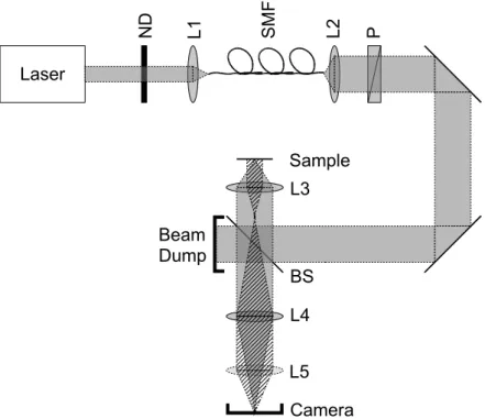
In order to gain more insight into the character of the resonance around 725 nm, we image the reflection of a strongly focused beam of light from the photonic crystal slab. Figure 4.2 shows a schematic overview of the setup used in the experiments. Light from a tunable picosecond Ti:Sapphire laser or from an external-cavity tunable diode laser is attenuated using neutral-density filters (ND), sent through a single-mode optical fiber (SMF), and collimated with a f = 5 cm lens to a beam of ∼ 1 cm diameter. The beam is polarization-filtered using a polarizer (P). A glass plate that is anti-reflection coated on one side is used as a beam splitter (BS) to direct the beam to an aspheric lens L3 (f = 8 mm, NA = 0.5), that focuses the light onto the photonic-crystal membrane. The membrane is aligned such that the beam axis is parallel to its surface normal. The reflection from the membrane is collected with the same lens and sent back onto the beam splitter. The reflected light is transmitted through this beam splitter, and the surface of the photonic crystal membrane is imaged onto a CCD camera using a f = 250 mm lens L4. A second lens L5 (f = 125 mm) can be inserted into the imaging setup, to make a k-space image of the photonic crystal reflection. The solid and hatched beam paths depicted in Fig. 4.2 show the imaging of the real-space andk-space reflection, respectively. A polarization analyzer was placed between lenses L4 and L5 to probe the polarization properties of the reflected light.
Laser
ND L1 SM
F
L2 P
L3
L4
L5
Camera BS Sample
Beam Dump
Figure 4.2. Experimental setup. Light from a tunable laser is focused on the photonic-crystal sample via a beam splitter (BS). By inserting the lens L5, the imaging is switched from real-space imaging (solid beam path) tok-space imaging of the reflection from the photonic crystal slab (hatched beam path). Details of the setup are found in the text.
4.4.1 k-space imaging and polarization properties
Figure 4.3(a) shows the recorded reflection in k-space, when the photonic-crystal slab was illuminated at a wavelength of 762.5 nm, red-detuned from the resonance at 725 nm, with horizontal polarization. Most obviously, a dark and bright ring pattern, that is centered around the normal-incidence (Γ) point (the center of the image) is visible. These Fabry-Perot fringes are caused by the partial reflection from the GaAs substrate underneath the photonic-crystal slab, that interferes with the reflection from the slab. The fact that the rings are concentric indicates that locally the membrane is parallel to the GaAs substrate.
4.4 Imaging of the resonance
a)
b)
c)
d)
resonance suggests that the resonance originates from the (±1,0) reciprocal lattice points. The resonances are not visible in the vertical direction. When the polarization of the illumination is rotated 90◦ (b), only the resonances in the(0,±1)direction are visible. A comparison with a calculation of the waveg-uide modes of a uniform slab with an effective refractive index (not shown), and folding these modes back into the first Brillouin zone, confirms that the resonance is caused by coupling to the TM0 waveguide mode, by diffraction from the (1,0) reciprocal lattice points. On changing the wavelength towards the blue, the resonances are observed to shift towards theΓ-point. This allows us to identify this resonance with the resonance around 725 nm, observed in the normal-incidence reflection spectrum.
Figures 4.3(c) and (d) show a polarization analysis of the reflection for vertically polarized light. In Fig. 4.3(c), an analyzer is placed parallel to the polarization of the incident light. In Fig. 4.3(d), the analyzer is placed per-pendicularly. Most of the reflected light is polarized the same as the incident light, except for four small areas in the (diagonal) ΓM-directions. Along the directions of high symmetry, the resonances of a photonic-crystal slab can be characterized by the polarization properties of the radiating field, as either s-orp-polarized [38]. The incident polarization is aligned with theΓX symmetry direction, such that it isp-polarized in the vertical, ands-polarized in the hor-izontal direction. Since these are the eigenpolarizations of the resonant modes, no polarization mixing occurs and the reflected light has the same polarization as the incident light. Away from the ΓX directions, the incident light is both s- andp-polarized, nor polarized in an eigenpolarization of the resonant mode. Light that is coupled into the leaky waveguide mode will therefore undergo a polarization rotation, which shows up in the k-space image with crossed polarizers [Fig. 4.3(d)].
4.4.2 Real space imaging
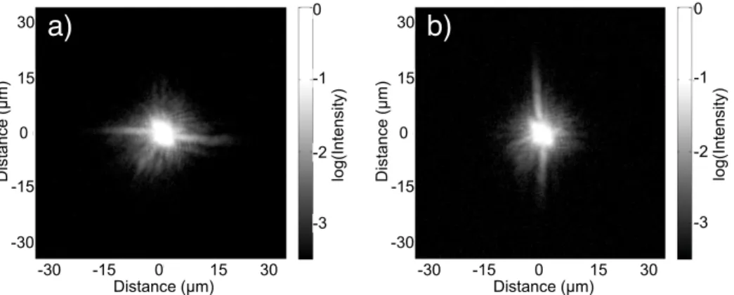
propa-4.4 Imaging of the resonance
gates in the direction of the group velocity, which is not necessarily the same as the direction of the reciprocal lattice vector that causes the resonance [47, 48].
b)
a)
-30 -15 0 15 30
Distance (!m) -30 -15Distance (0 !m)15 30
-30 -15 0 15 30 Di sta nc e ( ! m) -30 -15 0 15 30 Di sta nc e ( ! m) -3 -2 -1 0 log (I nten si ty ) -3 -2 -1 0 log (I nten si ty)
Figure 4.4. Real space image of the reflection of the photonic-crystal slab, when illuminated at a wavelength of 762.5 nm, on a logarithmic scale, for horizontally (a) and vertically (b) polarized illumination. The two long tails that emerge from the pump spot are caused by light that is resonantly coupled to a leaky waveguide mode of the slab, and that decays exponentially from this waveguide mode.
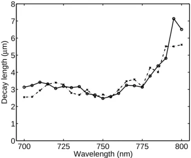
In Fig. 4.5 we show a cross-section of the vertical resonance of Fig. 4.4(b). To obtain this plot, we summed the intensity over a horizontal box of width 4.5 µm, in order to capture all intensity in the resonant tails. In this im-age, the direct and resonant contributions to the Fano resonance are spatially separated [49]. The central peak is Gaussian in shape, and corresponds to a direct image of the illuminating spot. As a comparison, the reflection from an unpatterned piece of the sample is given as the dash-dotted curve, showing a perfect agreement with the peak of the measured curve. The resonant tails decay exponentially on both sides of the central spot. A fit of a single expo-nential to these tails is shown by the dashed lines. The resonant contribution can be traced over 2.5 orders of magnitude, and up to a distance of 30 µm away from the center of the illumination spot. An interference between the resonant and non-resonant contributions, as observed in similar experiments with surface-plasmon polaritons [49], was not observed in these measurements. We measured the real-space image of the resonance for different wave-lengths from 700 to 800 nm. From these images, we obtained the decay length of the resonant contribution by fitting a single exponential to the intensity of the resonant tail. The result of these fits are shown in Fig. 4.6 and varies from
!45 !30 !15 0 15 30 45 !4
!3 !2 !1 0
Distance (µm)
log(Intensity)
Figure 4.5. Logarithmic plot of the measured reflected intensity, taken along the vertical resonance in Fig. 4.4(b) (solid curve). The two con-tributions to the Fano resonance are spatially separated. The reflection arising from the direct (Fresnel) contribution is giving rise to the central spot, whereas the exponentially decaying tails are caused by light that is resonantly coupled to a waveguide mode. The dashed lines show a linear fit to the resonant tails. The dash-dotted curve is the profile of the pump spot, measured on an unpatterned region of the substrate.
The decay length lof the resonant tails can be parametrized by l= vg
γ+ Γ = λ
2πngQ, (4.2)
4.4 Imaging of the resonance
700 725 750 775 800
0 1 2 3 4 5 6 7 8
Wavelength (nm)
Decay length (
µ
m)
Figure 4.6. Decay length of the TM0(1,0) resonance as a function of
wavelength. The circles and crosses show the fitted decay length on either side of the non-resonant reflection spot. The lines are guides to the eye.
of incidence, we expect this resonance to split, and obtain a branch that shifts to lower wavelengths. Since this resonance can be linked to a TE waveguide mode, however, we do not expect this resonance to couple strongly to the TM-like resonance that is described in the rest of this chapter.
4.5
Conclusion
Part II
Chapter 5
Enhanced coupling between plasmons
in hole arrays with periodic dielectric
antennas
We compare the angle-dependent transmission spectra of a metal hole array with dielectric pillars in each hole with that of a con-ventional metal hole array. The pillars enhance the optical trans-mission as well as the interaction between surface-plasmon modes. This results in an observed splitting ∆ω/ω as large as 6%, at nor-mal incidence, for the modes on the pillar side of the array.
This chapter is based on D. Stolwijk, E. F. C. Driessen, M. A. Verschuuren, G. W. ’t
Hooft, M. P. van Exter, and M. J. A. de Dood,Enhanced coupling of plasmons in hole arrays