Integrated Magnetic Memory for Embedded Computing Systems
Kenneth J. Hass, Gregory DonohoeUniversity of Idaho 721 S Lochsa St Post Falls, ID 83854, USA
208-262-2009 kjhass,[email protected] Yang-Ki Hong University of Alabama Box 870286 Tuscaloosa, AL 35487, USA 205-348-7268 [email protected] Byoung-Chul Choi University of Victoria PO Box 1700 STN CSC Victoria, BC V8W 2Y2, Canada
250-721-7731 [email protected]
Kelly DeGregorio, Richard Hayhurst American Semiconductor, Inc.
3100 S. Vista Ave. Ste 230 Boise, ID 83705, USA
kellydegregorio,[email protected]
Abstract—This paper describes a new nonvolatile memory technology being developed for embedded computing. Based on a Magnetic Tunneling Junction (MTJ) cell, these devices will be integrated into a radiation-hard SOI CMOS process, to replace conventional flip flops and small on-chip memories. These nonvolatile memory cells will form an integral part of on-chip power management.
Memory density is the primary driver for commercial MRAMs, which are designed using an X-Y addressing scheme. Current pulses on two orthogonal wires generate a magnetic field, which is strong enough to reprogram a cell at the intersection between the two wires, and nowhere else. This requires that the cells be very uniform in their sensitiv-ity, and optimized for magnetic “selectivsensitiv-ity,” so that only the desired cells are programmed.
Designed as replacements for flip-flops and latches, the Em-bedded Magnetic Memory uses a pair of MTJ cells in a dif-ferential scheme. The difdif-ferential arrangement mitigates con-cerns of process variation, but introduces a new set of chal-lenges. Each cell will be programmed by a single current pulse. The challenge is to design the cells and the program-ming structures to make efficient use of the magnetic field,
1-4244-0525-4/07/$20.00©2007 IEEE
IEEEAC paper #1464, Version 3, Updated October 20, 2006
and minimize programming current.
T
ABLE OFC
ONTENTS1 EMBEDDEDNONVOLATILEMEMORY. . . 1
2 MAGNETICMEMORY. . . 2
3 RADIATIONEFFECTS INMTJS. . . 3
4 EMBEDDINGNONVOLATILEMEMORYCELLS. 4 5 CONCLUSIONS. . . 7
6 ACKNOWLEDGEMENTS. . . 7
REFERENCES. . . 8
BIOGRAPHY. . . 10
1. E
MBEDDEDN
ONVOLATILEM
EMORY There are several unique applications for embedded non-volatile memory in aerospace systems. They derive from the special functional requirements of these applications as well as the unusually harsh enviroments in which they must oper-ate.Circumvention
In situations where electronic systems may be exposed to very short but intense bursts of ionizing radiation, such as nuclear blasts in a space environment, a common problem is
that extremely high photocurrents are generated within the in-tegrated circuit. If the voltage drop along the circuit’s power supply wiring approaches the nominal supply voltage then the effective supply voltage falls to zero, which is referred to as “rail span collapse” [1]. At higher dose rates the pho-tocurrents may cause permanent damage to power supplies or distribution networks. For some integrated circuit technolo-gies destructive latchup conditions can also occur during a transient dose. A common technique for avoiding transient dose failure is known as circumvention, and involves remov-ing power from the system within a very short period of time, perhaps microseconds, after a nuclear event is detected. Whether power is lost because of rail-span collapse or cir-cumvention, conventional static RAM cells and flip flops will lose their stored information. Critical data must be stored in some kind of non-volatile memory so that it can be recovered after the transient radiation ends. Desirable characteristics for the non-volatile storage in this application would include a short write time and low sensitivity to total dose effects. Personalization
The trend in many aerospace applications is toward pro-grammable integrated circuits, such as a Field Propro-grammable Gate Array (FPGA). The cost of designing, manufacturing and qualifying and integrated circuit can then be amortized over many users. Programmable hardware also allows de-signers to field systems much more quickly and to adapt to changing requirements. In many cases it is desirable to store the unique programming, or personalization, of a circuit in non-volatile memory so that it begins performing its desired function immediately when power is applied. Non-volatile personalization also saves power in situations where the sys-tem is only activated for a brief period of time and then sleeps in an unpowered state until it is needed again.
For personalization applications, the write time of the non-volatile memory is not a critical parameter since writing is infrequent. A more important characteristic is the memory’s long term reliability and immunity to radiation effects. Since the memory bits are often scattered amid functional logic blocks it is not practical to use the error-correcting codes that are common in bulk memory.
Cryptographic Systems
Cryptographic systems represent a small but important niche. They typically require a small amount of critical data, such as a key or password, to be stored reliably for long periods of time. If the security of the system has been compromised or if tampering is detected it could be necessary to erase the cryptographic information as quickly as possible and with as little energy as possible.
2. M
AGNETICM
EMORYIn ferromagnetic materials the conduction electrons are spin polarized, meaning that their quantum spin states are
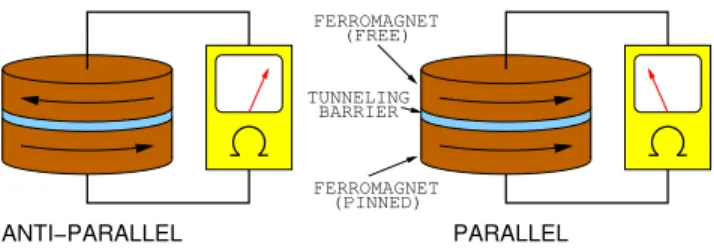
predom-inantly aligned with the magnetic dipole of the material sam-ple [2, 3]. Since the Pauli exclusion princisam-ple applies to spin, tunneling between two ferromagnetic layers separated by a very thin insulator is dependent on the relative alignment of their magnetic moments. If the magnetic dipole moments of the two layers are aligned in a parallel fashion then the pre-dominant spin state of the electrons on one side and the va-cancies on the other will be the same, and tunneling should occur freely (see Fig. 1). On the other hand, if the magnetic moments of the conducting layers are antiparallel then the
ANTI−PARALLEL TUNNELING BARRIER PARALLEL FERROMAGNET FERROMAGNET (FREE) (PINNED)
Figure 1. Magnetic Tunneling Junction
tunneling current should be reduced. Thus, the effective re-sistance of the tunneling junction will depend on the relative alignment of the ferromagnetic layers on either side of it. A key parameter of MTJs is the tunneling magnetoresistance ratio (TMR), which is defined as
T M R= RAP −RP
RP (1)
where RAP is the resistance of the junction when the
mag-netic fields have antiparallel orientation andRP is the
resis-tance when the fields are parallel. Room-temperature TMR values of 30% to 50% are typical [4, 5]. and values as high as 410% have been reported [6]. The actual resistance of the MTJ is primarily determined by its area and the thickness of the insulating layer, with values of tens of kilohms commonly used in solid state memories to reduce power but maintain fast operation.
Data bits are stored in the MTJ by switching the orientation of the free (soft) ferromagnetic layer, while the pinned (hard) ferromagnetic layer remains unchanged. The pinned layer has a very high coercivity and is magnetized during wafer fab-rication, giving it the same field orientation in all MTJs. The free layer has a low coercivity so its field orientation can be altered by passing current through wires adjacent to the MTJ and generating the necessary magnetic field. The very thin oxide layer grown between the free and pinned layers serves as the tunneling barrier. The thinness of the oxide limits the voltage that can be reliably applied across the junction to a few hundred millivolts, which requires careful circuit design to prevent permanent damage [7].
The size and shape of the MTJ is critical for proper switch-ing of the free layer’s magnetic moment [8–11]. Ideally, the free layer would uniformly and rapidly reorient its magnetic moment to an applied field. In reality the switching is not
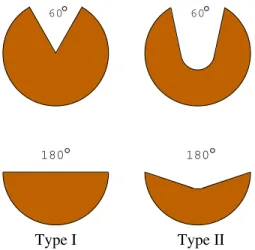
isotropic, with the edges and ends of the free layer shape playing a large role. Some shapes have stable states where two or more magnetic domains may exist. Micromagnetic studies have been performed on a wide variety of shapes, in-cluding rectangles, ellipses, hexagons, circles, and rings. This research will use the “Pac-man” shape, which has been shown to have reliable and uniform domain reversal [12–15]. Two variations of the Pac-man, shown in Fig. 2, have been studied and the best results were obtained from the type II shape and elongated type I with a 180° slot angle.
180 180
60 60
Type I Type II
Figure 2. Pac-man-shaped Ferromagnetic Elements
3. R
ADIATIONE
FFECTS INMTJ
S Total Ionizing Dose EffectsTotal ionizing dose (TID) effects are the result of accumu-lated damage in materials and change the characteristics of the material for long periods of time [16]. In digital inte-grated circuits the TID effects are seen as trapped charge in oxide layers because when an atom in an insulator is ionized the free electron will often be swept away by electric fields before recombination can occur, leaving behind a relatively fixed positive charge. Damage occuring at the interface be-tween silicon and a gate oxide can also appear as a fixed neg-ative charge by trapping holes.
Floating gate memory technologies, such as Flash, can be se-riously degraded by TID [17]. Information is stored by using tunneling through thin insulators to deposit charge on an un-connected, or “floating”, gate electrode, thereby altering the threshold voltage of the associated transistor. The electrons and holes created by the ionizing radiation tend to neutralize whatever charge was left on the floating gate during program-ming, rendering it impossible to successfully discern the ‘1’ state from the ‘0’ state. Failures have been seen with TID lev-els of around 100 krad(SiO2) in commercial Flash memories.
Unfortunately, scaling to thinner oxides in advanced devices does not necessarily eliminate this problem since the amount of charge representing the stored data will be reduced to tens or hundreds of electrons [18, 19].
Since MTJs do not rely on charge as a data storage phe-nomenon they are relatively insensitive to TID effects. Fur-thermore, the tunnel current will tend to fill trapped holes, repairing the damage caused by an ionizing event. The very thin Al2O3 films used in MTJs have demonstrated very
lit-tle damage from TID levels of several Mrad(SiO2) [20]. The
degradation due to TID is small compared to temperature and manufacturing variation so it is likely that existing MTJ mem-ory circuits will easily cope with TID effects.
Single Event Effects
Single event effects (SEE) include a variety of transient and permanent failures, with the common thread that they are caused by a single, highly energetic particle that passes through a circuit. As the particle travels through a material it can ionize atoms, creating a trail of charge. The amount of charge left behind depends on the mass and energy of the particle, as well as the nature of the material through which it passes. Years ago, the release of alpha particles (helium nuclei) from naturally occurring radioactive decay in pack-aging materials resulted in transient failures in commercial integrated circuits.
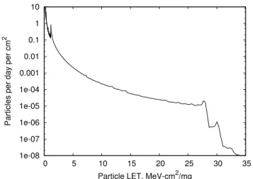
In the space environment, the SEE threat varies significantly with the altitude and orientation of orbit, or with the path of a deep space mission. The most common particles of interest are protons and electrons that have been trapped and accel-erated in the earth’s magnetic field, creating the Van Allen radiation belts. Of these, protons have sufficient momentum to cause SEE in electronics. The outer Van Allen belt also traps significant numbers of heavier particles called galactic cosmic rays (GCR) which are the nuclei of naturally occur-ing elements. At large distances from earth the primary threat is from GCR, although radiation belts can be found around other bodies that have a magnetic field. The probability of encountering a particle of a given mass falls off rapidly as the mass increases, with a steep decline for elements heavier than iron, as shown in Fig. 3 [21]. As a general rule, elec-tronic systems should be immune to SEE from protons for use in space and few applications require immunity to parti-cles heavier than iron.
As with TID, floating gate memories are susceptible to data loss caused by SEE. One proposed model for these failures is that by ionizing atoms along its path the particle creates a conductive “pipe” between the floating gate and the control gate of the transistor, thus draining the stored charge [22]. Measurable charge loss can result from the strike of a single alpha particle, so this is a reliability concern for almost any space application. Again, it appears that this effect will only become more pronounced as device geometries shrink and the amount of charge stored on the floating gate is reduced. Permanent changes have also been observed in floating gate cells, where the retention characteristics of the cell are signif-icantly degraded [18].
1e-08 1e-07 1e-06 1e-05 1e-04 0.001 0.01 0.1 1 10 0 5 10 15 20 25 30 35
Particles per day per cm
2
Particle LET, MeV-cm2/mg
Figure 3. Typical Cosmic Ray Spectrum
can cause permanent and significant damage to thin insulat-ing films. If a large electric field is applied across the insulator and heavy ion passes through it, a catastrophic failure known as single event gate rupture (SEGR) can occur [23, 24]. For-tunately, only low bias voltages are used with MTJs. Tests performed with heavy ions demonstrated a small decrease in the tunneling magnetoresistance and no observable change in the magnetic layers [25].
4. E
MBEDDINGN
ONVOLATILEM
EMORYC
ELLSThe goal of this work is to develop a magnetic memory cell, or latch, which can be used in a generic digital design to replace replace conventional latches in a circuit when non-volatile storage is needed. Unlike an MRAM, these latches will be interspersed with logic functions. They will be com-patible with conventional design tools for integrated circuit synthesis and physical design.
Retrieving information stored in MTJs requires that several conflicting constraints be met simultaneously. In order to sense the resistance of the MTJ we must apply a voltage across it and allow current to pass through. For improved signal-to-noise ratios the applied voltage (and current) should be increased, but doing so will increase power consumption. Even a static current of 1 µA in each MTJ would be pro-hibitive in a large integrated circuit. Furthermore, bias volt-ages across the MTJ should be kept well below 1 V to insure long term reliability [26–30]. The resistance difference be-tween the parallel and antiparallel states is also reduced as the bias voltage increases, providing additional incentive to use low voltages [31, 32].
Typical magnetoresistance ratios are smaller than the normal spread in circuit parameters due to manufacturing variations and operating conditions so it is not possible to reliably sense the MTJ’s state (parallel or antiparallel) by measuring its ab-solute resistance. Therefore, practical approaches to mag-netic memories commonly use a reference circuit that
rep-resents a resistance equal to a midpoint between the two pos-sible MTJ states [33,34]. An alternative scheme employs two MTJs with opposite states in each memory bit and compares them [35–37].
Magnetic Latches
We have developed two proposed latch designs that com-bine MTJs with SEE-resistant circuits for embedded mag-netic memory cells. The first is a differential sensing latch that uses the MTJ resistance to provide SEE resistance [38].
VDD RD Q6 B Q5 R Q RD Q4 L QN Q1 Q3 Q2 MTJ1 MTJ2
Figure 4. Dual-MTJ latch cell schematic
The circuitry needed to read the cell’s logic state is shown in Fig. 4. The two MTJ elements are shown as variable re-sistancesMTJ1andMTJ2. Above the MTJs are two cross-coupled PMOS transistors,Q1andQ2, and below them are two cross-coupled NMOS transistors,Q4andQ5. These four transistors comprise a static latch. If the MTJs were replaced by wires the four transistors would then form the simple two inverter latch that is the heart of CMOS static RAM cells. However, in this cell the desired state is written magnetically, rather than electrically, by altering the magnetoresistance of the MTJs. TransistorsQ3andQ6, along with the signalRD, allow the difference in resistance betweenMTJ1andMTJ2 to set the state of the static latch formed by the cross coupled transistors. The true and complemented logic levels corre-sponding to the stored state are then available on theQand QNoutput signals.
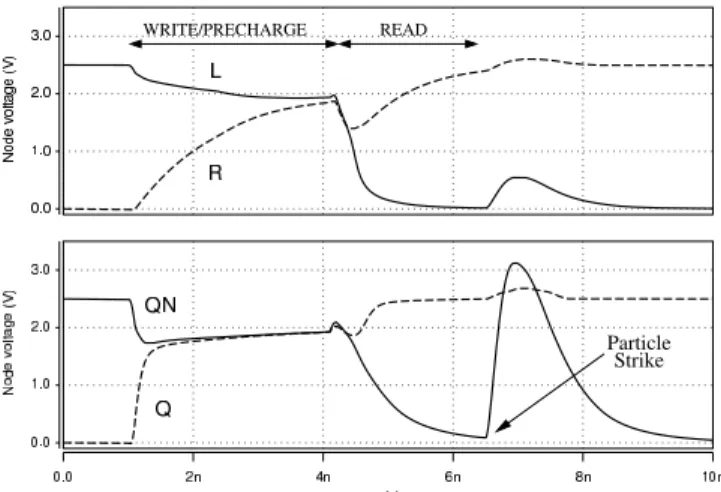
The cell’s read operation has been simulated in HSPICE, as shown in Fig. 5. Transistor parameters were for a commer-cial 0.25 µm CMOS process and all transistors have a width of 3.0 µm and a length of 0.24 µm exceptQ6, which is 0.5/0.5. The TMR is assumed to be 50% with a parallel resistance of 20 kΩ. In this simulation the PMOS and NMOS
transis-tor models are for the TSMC 0.25 µm CMOS process and operate with a nominal supply voltage of 2.5 V. MTJ1and MTJ2are modeled as fixed resistors with values of 16.5 kΩ
and 15.0 kΩ, respectively, in parallel with a 10.0 fF capacitor.
Initially,Qis low andQNis high, so the cross-coupled tran-sistors are storing a logic ‘0’ value. RDis initially asserted soQ3is disabled whileQ6is conducting. Very little current flows through the MTJs under these conditions, so nodesL andQNare at the same voltage and nodesRandQare at the same voltage.
WhenRDis deasserted at 1 nsQ3becomes conducting while Q6is disabled and all nodes begin to rise. Q1andQ2will source current until QandQN rise toVDD −VT P, where
VDDis the supply voltage andVT P is the threshold voltage
of the PMOS transistors. Similarly, Q4 andQ5will allow nodeBto rise to approximatelyVDD−VT P −VT N.Q3
ef-fectively shortsQandQNtogether so they will rise together. WithoutQ3a much longer time period would be required to equalize these voltages, which is essential to resolving the small difference in MTJ resistance.
WhenRDis asserted again at about 4 nsQ3is disabled while Q6is enabled, bringing nodeBto ground. Now the gate volt-age,VGS, ofQ4andQ5is much greater than their threshold
voltage so these transistors start conducting current, limited by the MTJ resistances. In this simulationMTJ1has a higher resistance (30 kΩ) so less current flows into nodeLand this
node falls slightly faster than nodeR. As Lfalls it tends to reduce the VGS of Q5so this transistor will sink less
cur-rent, reinforcing the∆Rof the MTJs with positive feedback
to keep node R high. Since Q4 remains active it will be-gin to sink current throughMTJ1and start to pull nodeQN low, whereas little current flows through MTJ2 because of the lowVGS atQ5. AsQNfalls,Q2conducts more current
and brings nodeQup toVDD. As nodeQrises Q1will be
disabled so the cross-coupled PMOS transistors also provide positive feedback to reinforce∆R. All the nodes in the cell
soon rise toVDD or fall to ground, and the cell achieves a
stable state with virtually no static power dissipation and no voltage across the MTJs.
Note that in a quiescent state, during either a read or write op-eration, there is no voltage across the MTJs. While switching from one state to the other a voltage is applied to the MTJs but this is typically less than 1 V and has a duration of less than a nanosecond.
The critical single-event hardening of the proposed memory cell is achieved by serendipitous use of the high resistance of the MTJs themselves to provide decoupling, so that nodesQ, QN,LandRbecome four independent and redundant storage nodes. The simulation in Fig. 5 illustrates how the memory cell recovers from a cosmic particle strike to a PMOS transis-tor.
In this simulation the drain ofQ1, connected to node QN, receives the injected charge at 6.5 ns.QNquickly rises from near ground to aboveVDD. SinceQNis also connected to the
Particle Strike
WRITE/PRECHARGE READ
Figure 5. Simulated cosmic particle strike to PMOS of dual-MTJ cell
gate ofQ2the disturbance is capacitively couple toQ, but this coupling does not moveQtoward an invalid state. The high voltage on QNalso reducesVGS onQ2so that this
transis-tor is no longer able to source current intoQ. Fortunately, the correct level is maintained onQbecause of the parasitic ca-pacitance at this node. The resistance ofMTJ1isolates node L from the single event at QN, which is critical because if the voltage onLrises sufficiently that theVGS of transistor
Q5 becomes greater thanVT N then this transistor will sink
current (unopposed by Q2) and pull nodesRandQlow. If nodesRandQshould be pulled low beforeQNreturns to its correct state then an SEU will occur. However, in this sim-ulation nodeLremains low and nodesRandQremain high so the feedback from these three valid nodes is able to restore the correct state on nodeQN. Within about 2 ns the deposited charge is dissipated and the cell has fully recovered.
Although these simulations were performed with a TMR of 50%, the latch circuit can work with lower values if the par-asitic capacitances are carefully balanced and a longer read time is allowed. Higher values of resistance yield improved immunity to cosmic particles at the expense of longer read times.
The resistance value of the MTJs is related to the radiation tolerance of the cell in two ways. A high resistance value in-creases the decoupling between the NMOS and PMOS tran-sistors, so that the cell is immune to larger voltage transients from heavier or more energetic cosmic particles. Unfortu-nately, the correct state of the cell is restored by current flow-ing through a MTJ so larger resistance values also will delay the recovery of the cell. The parallel capacitance of the MTJ is also a factor since the single event transients tend to have very fast edges, and it is important to carefully model the MTJ and all parasitic capacitances in the cell.
The second proposed latch design is a magnetic shadow RAM and takes advantage of an independent double-gate (IDG) CMOS technology developed at American Semiconductor,
Inc. [39–41] A shadow RAM integrates a non-volatile stor-age cell into a conventional RAM cell, so that during normal operation the memory cell has the desirable speed and power characteristics of a static RAM. When desired, the contents of the static RAM can be transferred into the non-volatile shadow memory for retrieval at a later time. This capability is particularly attractive for circumvention applications, so that the operating state of the device can be easily restored after a nuclear event.
Combining MTJs with the Flexfet™ IDG CMOS transistors provides unique circuit design opportunities. This is a silicon-on-insulator process, and the transistors are used as four ter-minal devices. In conventional MOS transistors the fourth terminal would be the transistor body or substrate, but in this case the Flexfet™ functions more like a parallel MOSFET and JFET where the fourth terminal is the JFET gate. Phys-ically, the JFET gate is formed on the insulating substrate and is known as the “bottom gate”. The FET channel is de-posited on top of the bottom gate and then the “top gate”, the normal MOSFET gate, is formed on top of the channel layer. Altering the bottom gate voltage causes a nearly pro-portional change in the MOSFET threshold voltage, which in turn varies the drain current. For example, changing the bot-tom gate voltage from 0.0 V to 0.5 V decreases the MOSFET (top gate) threshold from 0.425 V to 0.0 V, a much larger shift than could be accomplished using the MOSFET body effect. Of course, since the bottom gate is a PN junction the circuit designer must avoid forward-biasing. The Flexfet™ technol-ogy has also demonstrated a high level of radiation tolerance, which complements the inherent tolerance of the MTJ. The information-storing circuitry of the shadow RAM cell is shown in Fig. 6 [42]. Because the achievable
magnetoresis-VDD
Q1
Q3
Q4
Q2
MTJ1
MTJ2
DATA
Q5
LDN
DATAN
Figure 6. Shadow RAM Cell
tance ratio is smaller than the normal variation in circuit ele-ments due to manufacturing and the environment, two MTJs programmed to opposite magnetic states (one parallel and the other antiparallel) are used. Differential sensing can then de-termine the relative resistance of the two MTJs. The MTJs
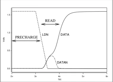
are shown as variable resistances MTJ1andMTJ2 and are connected to the bottom gate of NMOS transistors Q1and Q2. With PMOS transistorsQ3andQ4the circuit strongly resembles a conventional cross-coupled inverter RAM cell. (For clarity, the access transistors and the bottom gate con-nections to the PMOS transistors are not shown.) When the load signal,LDN, is highQ5is turned off and all circuit nodes are discharged (see Fig. 7). WhenLDNfallsQ5is enabled,
READ
PRECHARGE
Figure 7. SPICE Simulations
pulling the sources ofQ3andQ4high and enabling them as well. The bottom gates ofQ1andQ2are also pulled high by capacitive coupling to the top gate and drain, then begin to fall as their capacitance is discharged through the MTJs. The MTJ with lower resistance will pull its associated transistor’s bottom gate down faster, giving this transistor less drive than the other NMOS and imbalancing the cell. Regenerative feed-back causes the cell to snap to the desired state, where there is no d.c. power consumption and no voltage across the del-icate tunnel insulators. The same approach can be applied to a single-event resistant latch design, such as the DICE cell, if greater immunity to cosmic rays is needed [43].
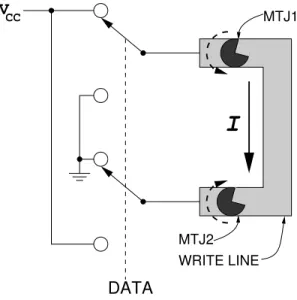
One-wire Programming
The circuitry and structures used to program an embedded shadow RAM are much different than those used in conven-tional bulk magnetic RAMs. Bulk magnetic RAM uses two orthogonal write lines, allowing conventional X-Y address-ing of individual bits [44, 45]. The net magnetic field at the intersection of a row write line and a column write line is the vector sum of the individual fields, which must be large enough to reorient the free layer. Although this arrangement allows for dense packing of the bits, it also means that a por-tion of the write field is applied to all of the bits on the se-lected row and all of the bits on the sese-lected column. There-fore, the design of these RAMs requires a careful compromise between minimizing the necessary write field (to reduce en-ergy consumption) and preventing write disturbances to the half-selected bits.
For an embedded MRAM, where the storage bits are inter-mixed with logic gates, the X-Y addressing scheme must be abandoned. Instead, a “one-wire” programming technique has been developed, as shown in the notional diagram of Fig. 8. This figure presents a top view of the MTJ elements
I
CC MTJ1 MTJ2 WRITE LINEV
DATA
Figure 8. One-wire Write Scheme
placed on top of the metal write line. The idealized switches illustrate how steering the current through the write line ac-complishes the programming of a ‘1’ or ‘0’ state. As shown, current flows first from left to right under MTJ1 and then from right to left underMTJ2. The dashed lines indicate the direction of the resulting magnetic field. Since the orientation of the pinned layer is fixed during manufacturing, and is the same for all MTJs, we must change the physical direction of current flow along the write line to program the two MTJs to opposite states.
In bulk MRAM cells the hard and easy axes of the free layer are typically aligned with the two orthogonal write lines. Consequently, the direction of the effective magnetic field is turned approximately 45° away from either write line. This configuration produces faster and more reliable switching of the free layer, with better selectivity, then if the magnetic field were directly aligned with the easy axis. In our one-wire pro-gramming scheme the net magnetic field is always at right angles to the write line, so the physical orientation of the cell is rotated to recreate the desired angle.
Suppose that the situation illustrated in Fig. 8 causesMTJ1 to have a parallel magnetic state whileMTJ2is forced to the antiparallel state, which we can arbitrarily declare to be the ‘0’ state of the memory bit. The switch shown in the diagram is implemented with transistors, and can reverse the overall current flow through the write line to program the opposite logical state of the memory bit. Reversing the current flow will reverse the direction of the magnetic fields, so thatMTJ1 is now in the parallel state andMTJ2is antiparallel, which
would represent the ‘1’ logical state of the memory bit. For a shadow RAM theDATAsignal that controls the switch is con-nected to theDATAsignal in Fig. 6 so the state of the static RAM portion of the cell will be stored in the MTJs, allowing a “snapshot” of the current information in the integrated cir-cuit to be saved for quick recovery after power is interrupted. The same concept can be used to quickly change the func-tion of programmable logic if theDATAsignal that controls the write line is distinct from the state of the static RAM so that a different personalization of the integrated circuit can be loaded in to the MTJs without disturbing the static RAM. The MTJs are actually quite thin (tens of nanometers) and placed directly on top of the write line, so that the magnetic field in their vicinity is almost entirely parallel to the top sur-face of the write line. This achieves the most efficient con-version of write current to useful magnetic field. The dis-tance from the MTJ’s free layer to any conductor other than the write line is much greater, so it is not difficult to prevent fields produced by adjacent wires from accidentally program-ming the cells.
Although Fig. 8 shows the write line connected directly be-tweenVCC and ground, in practice a number of write line
circuits can be connected in series and share the same pro-gramming current. Current would enter the write line circuit (from the previous bit in the serial string) at the node labeled
VCC and would exit the write line circuit (to the next bit in
the serial string) at the node shown connected to ground in the figure. The limit to the number of bits that can be strung to-gether in this fashion is determined by the voltage drop across each write line circuit, which is in turn determined by the size of the transistors that steer the current and the resistance of the write line itself. Micromagnetic simulations predict that a current of approximately 20 mA is needed for a typical alu-minum or copper line, but this can be reduced significantly by cladding the write line with a ferromagnetic material [46,47]. Fortunately, the write pulse is quite short compared to other nonvolatile memory technologies, lasting less than 5 nS.
5. C
ONCLUSIONSIntegrating magnetic memory elements into embedded com-puting systems enables a number of unique solutions for the requirements of aerospace applications. Magnetic memo-ries offer faster write time, lower power, improved reliability and superior radiation tolerance when compared to current floating-gate memories. However, successful use of MTJs requires careful attention to their characteristics as well as novel circuits. We have proposed two magnetic memory circuits that address these issues and can take advantage of independent-double-gate transistors.
6. A
CKNOWLEDGEMENTSThe authors wish to acknowledge the contribution of M. H. Park in the Materials Science and Engineering Depart-ment at the University of Idaho, and S. H. Gee and H. Han
in the Electrical and Computer Engineering Department at the University of Alabama, to the development of the Pac-man MTJ. The suggestions made by the reviewers were also greatly appreciated. This research was supported by the Air Force Research Laboratory under AFRL Grant F29601-04-1-0206.
R
EFERENCES[1] M. R. Ackermann and R. E. Mikawa, “Factors con-tributing to CMOS static RAM upset,” IEEE Trans. Nucl. Sci., vol. NS-33, no. 6, pp. 1524–1529, Dec. 1986. [2] G. A. Prinz, “Spin-polarized transport,”Physics Today,
pp. 58–63, Apr. 1995.
[3] ——, “Magnetoelectronics,” Science, vol. 282, pp. 1660–1663, Nov. 27, 1998.
[4] J. S. Moodera, L. R. Kinder, T. M. Wong, and R. Meser-vey, “Large magnetoresistance at room temperature in ferromagnetic thin film tunnel junctions,” Physical Re-view Letters, vol. 74, no. 16, pp. 3273–3276, Apr. 1995. [5] T. Miyazaki and N. Tezuka, “Spin polarized tunneling in ferromagnet/insulator/ferromagnet junctions,” Jour-nal of Magnetism and Magnetic Materials, vol. 151, pp. 403–410, 1995.
[6] S. Yuasa, A. Fukushima, H. Kubota, Y. Suzuki, and K. Ando, “Giant tunneling magnetoresistance up to 410% at room temperature in fully epitax-ial Co/MgO/Co magnetic tunnel junctions with bcc Co(001) electrodes,” Applied Physics Letters, vol. 89, no. 4, pp. 042 505–1–042 505–3, 2006.
[7] K.-S. Kim, B. K. Cho, T. W. Kim, and W. J. Park, “Junc-tion area dependence of breakdown characteristics in magnetic tunnel junctions,”Journal of Applied Physics, vol. 93, no. 10, pp. 8364–8366, May 2003.
[8] Y. Zheng and J.-G. Zhu, “Switching field variation in patterned submicron magnetic film elements,” Journal of Applied Physics, vol. 81, no. 8, pp. 5471–5473, Apr. 15, 1997.
[9] Y. Lu, P. L. Trouilloud, D. W. Abraham, R. Koch, J. Slonczewski, S. Brown, J. Bucchignano, E. O’Sullivan, R. A. Wanner, W. J. Gallagher, and S. S. P. Parkin, “Observation of magnetic switching in submicron magnetic-tunnel junctions at low fre-quency,”Journal of Applied Physics, vol. 85, no. 8, pp. 5267–5269, Apr. 1999.
[10] B. Warot, A. K. Petford-Long, and T. C. Anthony, “Magnetic properties of patterned tunnel junctions,” Journal of Applied Physics, vol. 93, no. 10, pp. 7287– 7289, May 15, 2003.
[11] C. C. Chang, Y. C. Chang, W. S. Chung, J. C. Wu, Z. H. Wei, M. F. Lai, and C. R. Chang, “Influences of the aspect ratio and film thickness on switching properties of elliptical permalloy elements,” IEEE Trans. Magn., vol. 41, no. 2, pp. 947–949, Feb. 2005.
[12] M. H. Park, Y. K. Hong, S. H. Gee, D. W. Erickson, and B. C. Choi, “Magnetization configuration and switching behavior of submicron NiFe elements: Pac-man shape,” Applied Physics Letters, vol. 83, no. 2, pp. 329–331, July 14, 2003.
[13] M. H. Park, Y. K. Hong, S. H. Gee, D. W. Erickson, T. Tanaka, and B. C. Choi, “Effect of shape anisotropy on switching behaviors of Pac-man NiFe submicron el-ements,”Journal of Applied Physics, vol. 95, no. 11, pp. 7019–7021, June 1, 2004.
[14] B. R. Pujada, B. C. Choi, M. H. Park, Y. K. Hong, S. H. Gee, H. Han, and G. W. Donohoe, “Micromag-netic configurations and switching mechanism in Pac-man-shaped submicron Ni80Fe20 magnets,”Journal of
Applied Physics, vol. 97, p. 073904, 2005.
[15] B. C. Choi, B. R. Pujada, Y. K. Hong, M. H. Park, H. Han, S. H. Gee, and G. W. Donohoe, “Micromag-netic domain structures and magnetization switching mechanism in submicrometer thin-film elements,”IEEE Trans. Magn., vol. 41, no. 10, pp. 3109–3111, Oct. 2005.
[16] R. L. Pease, “Total-dose issues for microelectronics in space systems,”IEEE Trans. Nucl. Sci., vol. 43, no. 2, pp. 442–451, Apr. 1996.
[17] G. Cellere, A. Paccagnella, A. Visconti, and M. Bo-nanomi, “Ionizing radiation effects on floating gates,” Applied Physics Letters, vol. 85, no. 3, pp. 485–487, July 19, 2004.
[18] G. Cellere and A. Paccagnella, “A review of ionizing ra-diation effects in floating gate memories,”IEEE Trans. Device Mat. Rel., vol. 4, no. 3, pp. 359–370, Sept. 2004. [19] G. Molas, D. Deleruyelle, B. D. Salvo, G. Ghibaudo, M. G´ely, L. Perniola, D. Lafond, and S. Deleonibus, “Degradation of floating-gate memory reliability by few electron phenomena,” IEEE Trans. Electron Devices, vol. 53, no. 10, pp. 2610–2619, Oct. 2006.
[20] J. A. Felix, J. R. Schwank, D. M. Fleetwood, M. R. Shaneyfelt, and E. P. Gusev, “Effects of radiation and charge trapping on the reliability of high-κ gate
di-electrics,” Microelectronics Reliability, vol. 44, pp. 563–575, 2004.
[21] Naval Research Laboratory. (2004, July 30) CREME96. [Online]. Available: creme96.nrl.navy.mil
[22] G. Cellere, A. Paccagnella, A. Visconti, M. Bonanomi, and A. Candelori, “Transient conductive path induced by a single ion in 10 nm sio2 layers,”IEEE Trans. Nucl. Sci., vol. 51, no. 6, pp. 3304–3311, Dec. 2004.
[23] L. W. Massengill, B. K. Choi, D. M. Fleetwood, R. D. Schrimpf, K. F. Galloway, M. R. Shaneyfelt, T. L. Meisenheimer, P. E. Dodd, J. R. Schwank, Y. M. Lee, R. S. Johnson, and G. Lucovsky, “Heavy-ion-induced breakdown in ultra-thin gate oxides and high-k di-electrics,” IEEE Trans. Nucl. Sci., vol. 48, no. 6, pp. 1904–1912, Dec. 2001.
[24] G. K. Lum, N. Boruta, J. M. Baker, L. Robinette, M. R. Shaneyfelt, J. R. Schwank, P. E. Dodd, and J. A. Felix, “New experimental findings for single-event gate rup-ture in MOS capacitors and linear devices,”IEEE Trans. Nucl. Sci., vol. 51, no. 6, pp. 3263–3269, Dec. 2004. [25] Y. Conraux, J. P. Nozi`eres, V. Da Costa, M.
Toule-monde, and K. Ounadjela, “Effects of swift heavy ion bombardment on magnetic tunnel junction functional properties,”Journal of Applied Physics, vol. 93, no. 10, pp. 7301–7303, May 15, 2003.
[26] W. Oepts, H. J. Verhagen, W. J. M. de Jonge, and R. Co-ehoorn, “Dielectric breakdown of ferromagnetic tunnel junctions,”Applied Physics Letters, vol. 73, no. 16, pp. 2363–2365, Oct. 19, 1998.
[27] W. Oepts, H. J. Verhagen, R. Coehoorn, and W. J. M. de Jonge, “Analysis of breakdown in ferromagnetic tun-nel junctions,” Journal of Applied Physics, vol. 86, no. 7, pp. 3863–3872, Oct. 1, 1999.
[28] K. Shimazawa, N. Kasahara, J. J. Sun, S. Araki, H. Morita, and M. Matsuzaki, “Electrical breakdown of the magnetic tunneling junction with an AlOx
bar-rier formed by radical oxidation,” Journal of Applied Physics, vol. 87, no. 9, pp. 5194–5196, May 2000. [29] J. Das, R. Degraeve, H. Boeve, P. Duchamps, L. Lagas,
G. Groeseneken, G. Borghs, and J. De Boeck, “Degra-dation and time dependent breakdown of stressed ferro-magnetic tunnel junctions,”Journal of Applied Physics, vol. 89, no. 11, pp. 7350–7352, June 1, 2001.
[30] D. Rao, K. Sin, M. Gibbons, S. Funada, M. Mao, C. Chien, and H.-C. Tong, “Voltage-induced barrier-layer damage in spin-dependent tunneling junctions,” Journal of Applied Physics, vol. 89, no. 11, pp. 7362– 7364, June 1, 2001.
[31] F. Li, Z. Li, M. Xiao, J. Du, W. Xu, and A. Hu, “Bias dependence and inversion of the tunneling magnetore-sistance in ferromagnetic junctions,”Physical Review B, vol. 69, pp. 054 410–1–054 410–8, 2004.
[32] S. T. Chui, “Bias dependence in spin-polarized tunnel-ing,”Physical Review B, vol. 55, no. 9, pp. 5600–5603, Mar. 1, 1997.
[33] A. Bette, J. DeBrosse, D. Gogl, H. Hoenigschmid, R. Robertazzi, C. Arndt, D. Braun, D. Casarotto, R. Havreluk, S. Lammers, W. Obermaier, W. Reohr, H. Viehmann, W. J. Gallagher, and G. M¨uller, “A high-speed 128kbit MRAM core for future universal memory applications,” inSymposium on VLSI Circuits Digest of Technical Papers, 2003.
[34] E. K. S. Au, W.-H. Ki, W. H. Mow, S. T. Hung, and C. Y. Wong, “A novel current-mode sensing scheme for magnetic tunnel junction RAM,” IEEE Trans. Magn., vol. 40, no. 2, pp. 483–488, Mar. 2004.
[35] K. Yamada, N. Sakai, Y. Ishizuka, and K. Mameno, “A novel sensing scheme for a MRAM with a 5% MR
ra-tio,” inSymposium on VLSI Circuits Digest of Technical Papers, 2001, pp. 123–124.
[36] T. Inaba, K. Tsuchida, T. Sugibayashi, S. Tahara, and H. Yoda, “Resistance ratio read (R³) architecture for a burst operated 1.5V MRAM macro,” inIEEE Custom Integrated Circuits Conference, 2003, pp. 399–402. [37] M. Aoki, H. Iwasa, and Y. Sato, “A novel voltage
sens-ing 1T/2MTJ cell with resistance ratio for highly stable and scalable MRAM,” inSymposium on VLSI Technol-ogy Digest of Technical Papers, 2005, pp. 170–171. [38] K. J. Hass, G. W. Donohoe, Y.-K. Hong, and B. C.
Choi, “Magnetic flip flops for space applications,”IEEE Trans. Magn., vol. 42, no. 10, pp. 2751–2753, Oct. 2006.
[39] S. Parke, M. Goldston, D. Hackler, K. DeGregorio, R. Hayhurst, A. Horvath, and S. Parsa, “Complemen-tary sidewall-spacer-diffused ultrashallow SD extension process for damascene independently-double-gated SOI CMOS,” inIEEE International SOI Conference, Oct. 4– 7, 2004, pp. 104–105.
[40] S. Parke, K. DeGregorio, M. Goldston, R. Hay-hurst, and D. Hackler, “Flexfet: A low-cost, rad-hard, independent-double-gate SOI CMOS technology with flexible, dynamic reconfigurability,” inIEEE Aerospace Conference, Mar. 5–12, 2005, pp. 1–8.
[41] S. Parke, K. DeGregorio, D. Hackler, and D. Wilson, “Ultra-low-power dynamic-threshold digital circuits in the flexFET independently-double-gated SOI CMOS technology,” in IEEE Workshop on Microelectronics and Electron Devices, Apr. 14, 2006, pp. 33–34. [42] K. J. Hass, G. W. Donohoe, Y.-K. Hong, B.-C. Choi,
K. DeGregorio, and R. Hayhurst, “Magnetic shadow RAM,” in Non-Volatile Memory Technology Sympo-sium, Nov. 5–8, 2006.
[43] T. Calin, M. Nicolaidis, and R. Velazco, “Upset hard-ened memory design for submicron CMOS technology,” IEEE Trans. Nucl. Sci., vol. 43, no. 6, pp. 2874–2878, Dec. 1996.
[44] J. M. Daughton, “Magnetic tunneling applied to mem-ory,” Journal of Applied Physics, vol. 81, no. 8, pp. 3758–3763, Apr. 15, 1997.
[45] B. N. Engel, N. D. Rizzo, J. Janesky, J. M. Slaughter, R. Dave, M. DeHerrera, M. Durlam, and S. Tehrani, “The science and technology of magnetoresistive tun-neling memory,” IEEE Trans. Nanotechnol., vol. 1, no. 1, pp. 32–38, Mar. 2002.
[46] M. Durlam, P. J. Naji, A. Omair, M. DeHerrera, J. Calder, J. M. Slaughter, B. N. Engel, N. D. Rizzo, G. Grynkewich, B. Butcher, C. Tracy, K. Smith, K. W. Kyler, J. J. Ren, J. A. Molla, W. A. Feil, R. G. Williams, and S. Tehrani, “A 1-Mbit MRAM based on 1T1MTJ bit cell integrated with copper interconnects,”IEEE J. Solid-State Circuits, vol. 38, no. 5, pp. 769–773, May 2003.
[47] Y. Asao, T. Kajiyama, Y. Fukuzumi, M. Amano, H. Aikawa, T. Ueda, T. Kishi, S. Ikegawa, K. Tsuchida, Y. Iwata, A. Nitayama, K. Shimura, Y. Kato, S. Miura, N. Ishiwata, H. Hada, S. Tahara, and H. Yoda, “Design and process integration for high-density, high-speed, and low-power 6F2
cross point MRAM cell,” in IEEE International Electron Devices Meeting Technical Di-gest, Dec. 13-15, 2004, pp. 23.2.1–23.2.4.
B
IOGRAPHYKenneth “Joe” Hass is a Sr. Re-search Engineer at the Center for Ad-vanced Microelectronics and Biomolec-ular Research at the University of Idaho. Mr. Hass obtained an M.S. degree in electrical engineering from Kansas State University in 1979. He began working in radiation hardened electronics at Sandia National Laboratories where he was a Distinguished Member of the Technical Staff. He is a Ph.D. candidate at the Univer-sity of Idaho and a member of IEEE.
Gregory Donohoehas been in aerospace R&D for 30 years. As a Senior Member of the Technical Staff at Sandia National Labs he worked in seismic signal pro-cessing, machine vision, and synthetic aperture radar data processing. He has held faculty and research positions at the University of New Mexico, Kestrel Cor-poration, and the Air Force Research Laboratory, Space Elec-tronics Branch. He his currently Research Associate Pro-fessor at the University of Idaho, working in reconfigurable computing and embedded magnetic memory. He holds a Ph.D. in Electrical and Computer Engineering from the Uni-versity of New Mexico.
Yang-Ki Hong received B.S. and M.S. degrees in physics and solid state physics (magnetism - Mossbauer spec-troscopy) from Yonsei University, Seoul, South Korea and a Ph.D. degree in met-allurgy (materials science) from the Uni-versity of Utah in 1981. He completed the Program for Management Develop-ment in 1992 from the Business School of Harvard Univer-sity. Prior to joining the University of Alabama as an E. A. ”Larry” Drummond endowed chair professor of Electrical and Computer Engineering, Hong was a Professor of Mate-rials Science and Engineering at University of Idaho, a Se-nior Vice President of OCI (now DCC) conglomerate group company in Seoul, South Korea, and an Assistant Professor of Auburn University. The research of Hong’s group has focused on magnetic random access memory, ferrite for RF devices, and magnetic nanoparticles for information data storage and biosensor applications.
Byoung C. Choi received the Diplom degree in Physics from Technical Uni-versity Aachen, Germany, and the Ph.D. degree from the Free University Berlin, Germany, in 1997. Following Research Fellowships at the University of Cambridge, U.K., and the University of Alberta, Canada, he became an As-sistant Professor at the University of Victoria, Canada, in the Department of Physics and Astronomy in 2002. He has worked for many years in the field of thin film magnetism. His main research interest concerns the nonequilibrium spin dy-namics in magnetic materials, with particular emphasis on magnetic nanostructures and multilayer films. He has co-authored about 70 papers.
Kelly DeGregorio’smost recent project has been the test chip design and layout to support the new Flexfet™ advanced SOI CMOS AS180FF process develop-ment for a test chip at American Semi-conductor Inc. Kelly’s chip design ef-forts have resulted in the ultra efficient SRAM CELL patent pending. Previously he worked under Dr. R. Jacob Baker for the MURI research group designing DC and RF novel noise circuits and mea-surements in a bulk CMOS process through MOSIS. He has experience in SOI design and measurement including collab-oration with Dr. Stephen Parke and the Boise State Univer-sity RF research group for designing novel transistors, ca-pacitors, and diodes. Mr. DeGregorio is knowledgeable of semiconductor processing and has first hand cleanroom ex-perience. Mr. DeGregorio holds a BSEE.
Rick Hayhurst is a Sr. Process Devel-opment Engineer who has worked in the semiconductor industry for 24 years. He has held several process ing, process-development and engineer-ing management positions for Western Digital, Motorola, and Zilog. Mr. Hay-hurst developed the base process used in Motorola’s Toulouse Bipolar facility. He developed the source/drain implant process in Zilog’s Mod I facility and authored the statistical process control (SPC) program used in Zilog’s fabrication facility. This SPC pro-gram has been copied by several semiconductor firms and is now considered an industry standard. He is currently supporting American Semiconductors research activity in a novel advanced silicon-on-insulator (SOI) rad-hard process technology for the development of American Semiconductors Flexfet™ SOI. Additionally, he was instrumental in the de-velopment of the “Novel Multilayer MIM Damascene Capac-itor” research project for the Missile Defense Agency respon-sible for defining the dielectric and electrode materials to be used. Mr. Hayhurst holds a B.S. in Mathematics, a BBA in General Business and ASET in Engineering Technology.