Performance Analysis of PV Standalone System with High-Power DC
–
DC
Converter Application to Induction Machine Drive
Shaik A Johny Begam
M.Tech Student ScholarDepartment of Electrical & Electronics Engineering, Krishnaveni Engineering College for Women,
Narasaraopet; Guntur (Dt); A.P, India.
G.Jyothi
Assistant ProfessorDepartment of Electrical & Electronics Engineering, Krishnaveni Engineering College for Women,
Narasaraopet; Guntur (Dt); A.P, India.
Abstract-. This paper presents a steady-state analysis of the bidirectional dual active bridge (DAB) dc–dc converter. This paper also presents the analysis of zero-voltage switching (ZVS) boundaries for buck and boost modes while considering the effect of snubber capacitors on the DAB converter is also presented. This is the new model for producing the equations for average and rms device currents. The proposed model can be used to predict the converter efficiency at any desired operating point. The proposed model was built for an aerospace energy storage application. The results obtained from the model under various voltages, currents and power transients verify converter operation and validate the proposed controller performance during bidirectional power transfer. Finally in this project the proposed converter is applied for standalone PVcell applications. The simulations results are carried by using MATLAB/SIMULINK SOFTWARE.
Key-Words: - DC-DC converter, Zero-voltage switching, average and rms device currents, High power density, Soft-switching operation, Galvanic isolation.
I.INTRODUCTION
In order to reduce weight, electrical power should be transmitted around the aircraft at a high voltage (HV) with Low current and low conduction losses. In this context, dc power distribution system architecture is found to be the most reliable configuration for sustaining aircraft operations even under severe supply transients [1], [2]. This technology leads to simpler equipment and enables significant energy savings [2], but requires high-power-density dc–dc converter for a variety of applications such as battery-based uninterrupted power sup- plies to mission critical aerospace applications, e.g., actuators and avionics. The dual active bridge (DAB) topology for dc–dc conversion has been popular among researchers over the past two decades due to its high performance, high efficiency, galvanic isolation, and inherent soft-switching property [3]. Subsequently several papers were published [2-6]These features make the DAB dc–dc converter a strong candidate for high-power-density aerospace applications.
Design considerations for high frequency transformers used in DAB converters were concerned with core material selection, loss minimization and realization of controlled leakage inductances as discussed in [7-8]. A comparative
evaluation of the DAB topology with other isolated converter topologies was reported in [9-10] and soft switching techniques to enhance the performance were presented in [11-14]. Various modulation techniques and control strategies to minimize the losses were investigated in [15-18]. This paper discusses the inherent soft-switching phenomenon of the DAB converter at high power and high frequency operating conditions. Bidirectional power flow capability is a key feature of DAB dc–dc converters, permitting flexible interfacing to energy storage devices. Although the DAB converter has an inherent soft-switching attribute, it is limited to a reduced operating range depending on voltage conversion ratio and output current. This is a drawback for applications that operate mainly with variable or low loads as the overall converter efficiency is reduced [18]–[21]. Recently, a model was proposed [21] for the DAB converter that has been validated under operating conditions for low load, low efficiency, and low power.
convert dc voltage into ac voltage and the other full bridge circuit operates as rectifier to convert ac voltage into dc voltage. The bi-directional dc to dc converter means the input dc supply is converted into ac and then dc by using two full bridge circuits. In one operation one full bridge circuit operate as rectifier in other operation it will operate as inverter similarly the second full bridge circuit will operate as rectifier in one operation and in the reverse operation it will operate as inverter. Both the converters are always in operating in rectifier mode or inverter mode so we can call as
dual active bridge and also the operation continues in both forward and reverse mode then we completely call as Bidirectional dual active bridge (DAB) dc-dc converter.
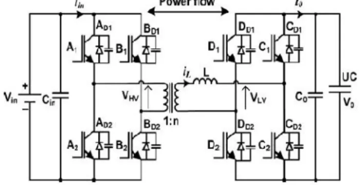
Fig. 1. Schematic of the DAB dc–dc converter.
Future aircraft are likely to employ electrically powered actuators for adjusting flight control surfaces and other high-power transient loads. To meet the peak power demands of aircraft electric loads and to absorb regenerated power, an ultra capacitor based energy storage system is examined in which a bidirectional DAB dc–dc converter is used. The DAB converter has various potential industry applications; hence, its performance has been investigated with the latest power switching devices such as SiC [27]. This paper presents the modeling, design, development, and performance evaluation of the DAB converter shown in Fig. 1, which can act as an interface between energy storage devices such as an ultra capacitor bank and the aircraft electrical power network. Ultra capacitors constitute one form of energy storage device, which can be used to meet transient power demands and smooth the load on the generators.
II. STEADY-STATE MODEL OF DAB CONVERTER
A. Basic Principle of Operation
In Future aircraft are likely to employ electrically powered actuators for adjusting flight control surfaces and other high-power transient loads. To meet the peak power demands of aircraft electric loads and to absorb regenerated power, an ultra capacitor based energy storage system is examined in which a bidirectional DAB dc–dc converter is used. The DAB converter shown in Fig. 1 consists of two full-bridge circuits connected through an isolation
transformer and a coupling inductor L, which may be provided partly or entirely by the transformer leakage inductance. The full bridge on the left hand side of Fig. 1 is connected to the HV dc bus and the full bridge on the right hand side is connected to the low-voltage (LV) ultra capacitor. Each bridge is controlled to generate an HF square-wave voltage at its terminals. By incorporating an appropriate value of coupling inductance, the two square-waves can be suitably phase shifted with respect to each other to control power flow from one dc source to another. Thus, bidirectional power flow is enabled through a small lightweight HF transformer and inductor combination, and power flows from the bridge generating the leading square-wave.
Although various modes of operation of the DAB converter have been presented recently for high power operation, the square-wave mode is supposedly the best operating mode. This is because imposing quasi-square-wave on the transformer primary and secondary voltages results in trapezoidal, triangular, and sinusoidal waveforms of inductor current in the DAB converter ac link. These modes are beneficial for extending the low-power operating range of the converter. Although these modes tend to reduce the switching losses, the voltage loss is significant due to zero voltage periods in the quasi-square-wave, which reduces the effective power transfer at high-power levels. Therefore, the contribution highlighted in this paper forms important research on the DAB converter.
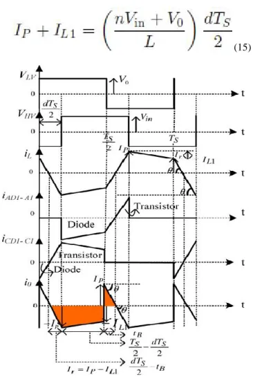
The key operating waveforms of the converter during buck mode, i.e., when power flows from the HV side to the LV side are shown in Fig. 2. The voltages generated by the two full bridges, VHV on the HV side and VLV on the LV side, are represented as square-wave voltages with 50% duty cycle. The current flowing through the coupling inductance is iL, iAD1-A1 and iCD1-C1 are the device currents on the HV and LV sides, respectively, and i0 is the output current. The time delay between VHV and VLV is dTS /2, where TS is the switching period and d is the duty ratio.
B. Steady-State Model
(1) Where n is the transformer turns ratio. Solving for the Lvswitching instant current based on the current slope during the interval dTS /2 gives
(2) In order to find the average output (ultra capacitor) current, the current expression is required for the interval tB: the time taken for iL to fall to zero following the HV bridge switching instant. Since the output current waveform is piecewise linear, this can be calculated from the following:
(3) Where θ is the angle marked on the i0 and iL current waveforms shown in Fig. 2. The total current change during the interval dTS /2, where the current is increased from -IP to IL 1,can be written as follows and the wave forms for the buck mode of the converter will be as follows.
Fig. 3. Operating waveforms of the DAB converter under buck mode
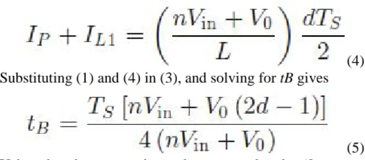
(4) Substituting (1) and (4) in (3), and solving for tB gives
(5) Using the above equations, the area under the i0 current waveform, shown as a shaded region in Fig. 2, is obtained. Since the waveform is periodic over half a cycle, dividing the area by the duration, which is TS /2, gives the average output current of the DAB converter, which may be expressed as follows:
(6) Normalizing the average output current by the base value nVinTS /2L gives
(7) From (7), by substituting the full control range (0 to 1) for the duty ratio d, it can be observed that maximum power transfer occurs for a duty ratio of 0.5. The inductor/transformer current wave shape is similar and is piecewise linear. Hence, to simplify the analysis, the waveform can be split into triangular or trapezoidal shapes over any time interval. The effective time intervals of those triangular and trapezoidal shapes were utilized to individually derive their rms currents and then summed together to obtain the total rms current equation of the DAB converter waveform. From Fig. 2, it can be observed that the inductor/transformer current is periodic and symmetrical over a cycle; hence, the rms value for a half cycle has been used to determine the corresponding value for a whole period. The instantaneous current I(t) over a half cycle is represented as follows:
TABLE I
RMS CURRENT MODEL OF DEVICES IN DAB CONVERTER FOR BUCK MODE (POWER TRANSFER
TABLE II
AVERAGE CURRENT MODEL OF DEVICES IN DAB CONVERTER FOR BUCK MODE (POWER TRANSFER
FROM THE HV SIDE TO THE LV SIDE)
Changing the limits to their effective intervals gives
Where Ir = IP− IL1 . Therefore, the rms equation of the inductor current is given by
(10)
Substituting I2 (t) in the above equation gives Irms as shown below.
Simplifying further, the final expression for the inductor/ transformer rms current during buck mode is expressed as shown (11)
(11)
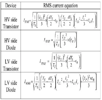
Similarly, the rms and average current model for devices on the HV and LV bridge sides of the DAB converter are derived from the waveforms shown in Fig. 2 and are listed in Tables I and II, respectively. When the converter operates in boost mode, power flows from the LV side to HV side. A similar procedure is followed to that of the buck mode to derive the necessary model. Converter operating waveforms under boost mode are depicted in Fig. 3. The voltage across inductor L over a half cycle is analyzed to determine the peak-to-peak change in inductor current. Subsequently, expressions are derived for inductor current at switching instants IP and IL 1 . The expression for current at the LV switching instant IL 1 is given as follows:
(12) Solving for the HV switching instant current based on the current slope during the interval dTS /2 gives
(13) To evaluate the average ultracapacitor current, an expression is required for interval tB : the time taken for iL to fall to zero following the LV switching instant. Since the i0 current waveform is piecewise linear, this can be calculated from the following:
(15)
Fig. 3. Operating waveforms of the DAB converter under boost mode
Substituting (12) and (15) in (14), then solving for tB gives
(16) Using the above equations, the area under the i0 current waveform, shown as shaded regions in Fig. 3, is obtained. Since the waveform is periodic over half a cycle, dividing the area by duration, which is TS /2, gives the average output current of the DAB converter as follows:
(17) Normalizing the average output current by the base value nVinTS /2L gives
(18)
Similar to (7), for the full control range of the DAB dc–dc converter, from (18) the maximum power transfer is found to occur at a duty ratio of 0.5. A similar procedure is followed to that of the buck mode in deriving the rms
current model. The rms value of inductor current and output current i0 can be derived using HV and LV switching instant current expressions and their respective time intervals, which result in (19)
(19)
The rms and average current model for devices on HV and LV sides of the DAB converter are derived from the waveforms shown in Fig. 3 and are given in Tables III and IV, respectively.
TABLE III
RMS CURRENT MODEL OF DEVICES IN DAB CONVERTER FOR BOOST MODE (POWER TRANSFER FROM THE LV SIDE TO THE HV SIDE)
TABLE IV
From the boost mode analysis, it can be observed that the corresponding expressions for the currents at the HV and LV switching instants, IP and IL 1 , respectively, in (1) and (2), are unchanged. However, in the expressions for i0 , the LV-side terminal current, given by (6) and (7), the (d−d2 ) term is replaced by (d2− d). Also, the expressions for the transistor and diode currents will be interchanged in Tables I and II. For example, the expression for the HV-side transistor current becomes the expression for the LV-side transistor with IP , IL 1 replaced by IL 1 , IP , respectively, and so forth.
C. ZVS Limits
If the transistor turn-OFF, resonance will naturally occur between device output capacitance and coupling inductance. The energy stored in the coupling inductance is sufficient to ensure charge/discharge of device output capacitances at the switching instants. The converter operating conditions to achieve virtually loss-less ZVS conditions are:
1) At turn-ON of any device, its anti parallel diode is conducting;
2) At turn-OFF of any device, the minimum current flow through the device is positive.
In practice, the ZVS limits will be slightly different due to the requirement for inductor current to be sufficient to ensure charge/discharge of the device output capacitances at the switching instants. By applying the ZVS conditions to the device current waveforms, shown in Fig. 2, the current at the LV switching instant must be greater than zero to achieve ZVS in the LV side bridge. Therefore, based on (2), the following condition must be satisfied for achieving ZVS in the LV side:
(20)
Solving for the inequality given in (20), the duty ratio at which ZVS occurs is obtained as follows:
(21)
Where V _ 0 = V0/nVin is the normalized voltage conversion ratio. To achieve ZVS in the HV Bridge, the current at the HV switching instant given in (1) must be positive. However, this condition is normally achieved and the limiting condition for ZVS is that given by (21).
For power transfer from the HV side to the LV side, (21) is applicable when V0’< 1. If V0’> 1, the shape of the inductor current in Fig. 2 will change, as shown in Fig. 3, and the effect of this is to interchange the expressions for the currents at the LV and HV switching instants. Therefore, with V0‘> 1, the expression for the LV
switching instant current is given by (1) and the expression for the HV switching instant current is given by (2). The ZVS limit still occurs in the LV Bridge, but is now specified by requiring the current level in (1) to be greater than zero, which leads to the following condition:
(22)
When the power transfers from the LV side to the HV side, the ZVS limit is again found to occur in the LV bridge and may be expressed by (20)–(22). Although turn-ON of transistors in the DAB converter is achieved at minimum (near-zero) positive diode current, the instantaneous transistor currents that occur during the turn-OFF process are significant. Normally, the device output capacitance is too low to produce a low dv/dt. Hence, minimal transistor currents during the turn-OFF switching time instant are mandatory in order to achieve low switching losses. To limit switching transients, reduce current/voltage spikes, and to minimize electromagnetic compatibility (EMC) problems associated with high dv/dt, snubber capacitors can be placed across the switching devices. These capacitors slow down the rate of voltage rise across the devices so that a lower voltage appears during the current decay time. Although snubber capacitors suppress voltage transients during switching, inclusion of a snubber across the switching transistors requires more energy to be stored in the coupling inductance to achieve soft switching [3]. The analysis was performed by assuming that the input (HV) and output (LV) voltages are constant during the transistor turn- OFF instants to estimate the minimum current necessary during turn-OFF to achieve ZVS. To achieve ZVS, energy stored in the inductor must equal the energy delivered to charge and discharge the snubber and device output capacitances. Kheraluwala et al. [3] and Naayagi [31] performed analysis to obtain an expression for the minimum inductor current during turn-OFF as follows:
Where L_ is the primary referred coupling inductance and v_
0 is the primary referred LV bridge voltage source. It has been assumed in the analysis that the insulated gate bipolar transistor (IGBT) tail current does not change when the snubber capacitor is added. The snubber creates oscillations due to the resonance induced between parasitic inductance of the IGBT module and the snubber capacitance during turn-OFF transient. In practice, the IGBT tail current may be reduced with the addition of an appropriate value of snubber capacitor. However, the tail time increases due to reduced dv/dt. Therefore, to simplify the analysis, the assumption that the IGBT tail current does not change with the inclusion of the snubber capacitor is made. The inductor current should be greater than or equal to the value of IL in (23) during transistor turn-OFF to achieve ZVS. This paper extends the analysis further to obtain the equations of duty ratio for HV and LV device ZVS limits for a specified value of snubber capacitor. Without the snubber, the condition to be satisfied for achieving ZVS during buck mode is given by (20). From (20) and (23), the ZVS boundary condition for V _ 0 < 1 while considering the inclusion of snubber is given by
(24) Solving for the above inequality, the duty ratio at which ZVS occurs for V _ 0 < 1 is given as follows:
(25) Similarly, for V _ 0 > 1, from (22) and (23), with the snubber,
the duty ratio at which ZVS occurs is given as follows:
(26) Equations (25) and (26) are unique and determine the ZVS boundary of the DAB converter for any value of snubber capacitor under buck and boost modes.
IV .MATLAB MODELEING AND SIMULATION RESULTS
Here simulation is carried out in three cases 1). Proposed High Power Step Up Bidirectional Converter. 2) Proposed High Power Step Down Bidirectional Converter. 3) Proposed High Power Step Down Bidirectional Converter with DC Machine Drive.
Case 1: Proposed High Power Step Up Converter.
Fig.4 Matlab/Simulink Model of Proposed High Power Step Up Bidirectional Converter.
As above Fig.4 shows the Matlab/Simulink Model of Proposed High Power Step up Bidirectional Converter.
Fig.5 Input Voltage, Output Voltage of Proposed DAB Converter in Boost Mode
Fig.5 shows the Input Voltage, Output Voltage of Proposed DAB Converter in Boost Mode.
Fig.6 shows the LV Side Current, Switch Current, Diode Current, and Inductor Current of Proposed DAB Converter in Boost Mode.
Fig.7 Hv Side Current, Switch Current, Diode Current of Proposed DAB Converter in Boost Mode.
Fig.7 shows the Hv Side Current, Switch Current, and Diode Current of Proposed DAB Converter in Boost Mode.
Fig.8 Input Voltage, Output Voltage of Proposed DAB Converter in Boost Mode
Fig.8 shows the Input Voltage, Output Voltage of Proposed DAB Converter in Boost Mode.
Case 2: Proposed High Power Step Down Converter.
Fig.9 Simulation results of the converter for Proposed High Power Step Down Bidirectional Converter
As Fig.9 shows the Simulation results of the converter for Proposed High Power Step Down Bidirectional Converter
Fig.10 Hv Side Current, Switch Current, Diode Current of Proposed DAB Converter in Buck Mode
Fig.11 Hv Side & Lv Side Transformer Voltages of Proposed DAB Converter in Buck Mode
Fig.11 shows the Hv Side & Lv Side Transformer Voltages of Proposed DAB Converter in Buck Mode.
Fig.12 Lv Side Current, Switch Current, Diode Current of Proposed DAB Converter in Buck Mode
Fig.12 shows the Lv Side Current, Switch Current, Diode Current of Proposed DAB Converter in Buck Mode.
Fig.13 Input Voltage, Output Voltage of Proposed DAB Converter in Buck Mode
Fig.13 shows the Input Voltage, Output Voltage of Proposed DAB Converter in Buck Mode.
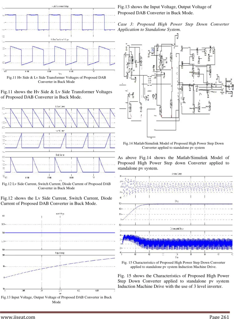
Case 3: Proposed High Power Step Down Converter Application to Standalone System.
Fig.14 Matlab/Simulink Model of Proposed High Power Step Down Converter applied to standalone pv system
As above Fig.14 shows the Matlab/Simulink Model of Proposed High Power Step down Converter applied to standalone pv system.
Fig. 15 Characteristics of Proposed High Power Step Down Converter applied to standalone pv system Induction Machine Drive.
Fig.16 Three Level Output Voltage
Fig.16 shows the Three Level Output Voltage of Proposed High Power Step down Converter applied to standalone pv system with the use of 3 level inverter.
V. CONCLUSION
This paper has presented a new steady-state model for the DAB converter. The square-wave operating mode of DAB is the best mode for high-power transfer. The proposed model produced key design equations for the square-wave mode of the DAB dc–dc converter. This paper has presented a new steady-state model for the DAB converter, operated in both buck & boost modes & same system is applied to Induction Machine Drive to check the performance using the three level inverter and supporting the load conditions without any voltage fluctuations, by using the standalone system with the help of battery energy based converter fed system. The square-wave operating mode of DAB is the best mode for high-power transfer. The proposed model produced key design equations for the square-wave mode of the DAB dc–dc converter. Expressions for average and rms device currents, along with peak and rms currents of the coupling inductor were obtained from the model. These equations are useful in predicting losses that occur in the devices and passive components and enable a study of the converter characteristics, in addition to aiding in the practical design of converter prototypes. The influence of the snubber capacitor was analyzed in detail and the minimum current required to operate the converter in the soft-switching region, and its corresponding duty ratio for buck and boost modes, has been determined.
REFERENCES
[1] B. Srimoolanathan, “Aircraft electrical power systems—
Charged with opportunities,” Aerospace and Defense Executive
Briefing of Frost & Sullivan, Frost & Sullivan, Mountain View, CA, Nov. 2008.
[2] Peter Fairley, The Smarter Grid, “Direct current networks gain ground,”Energy IEEE Spectr., Jan. 25, 2011.
[3] M. N. Kheraluwala, R. W. Gascoigne, D. M. Divan, and E. D. Baumann, “Performance characterization of a high-power dual active bridge DC-to-DC converter,”IEEE Trans. Ind. Appl., vol.
28, no. 6, pp. 1294–1301, Dec. 1992.
[4] K. Vangen, T. Melaa, A. K. Adnanes, and P. E. Kristiansen,
“Dual activebridge converter with large soft-switching range,” in Proc. Eur. Conf. Power Electron. Appl., 1993, vol. 3, pp. 328–333.
[5] R. Steigerwald, R. DeDonker, and M. Kheraluwala, “A
comparison of high-power dc-dc soft-switched converter
topologies,”IEEE Trans. Ind. Appl., vol. 32, no. 5, pp. 1139–1145, Sep. 1996.
[6] J. M. Zhang, D. M. Xu, and Z. Qian, “An improved dual active
bridgeDC/DC converter,” in Proc. IEEE Power Electron. Spec. Conf., Jun. 2001, vol. 1, pp. 232–236.
[7] J. Walter and R. W. De Doncker, “High-power galvanically isolated DC/DC converter topology for future automobiles,” in Proc. IEEE Power Electron. Spec. Conf., Jun. 2003, pp. 27–32.
[8] F. Krismer, J. Biela, and J. W. Kolar, “A comparative
evaluation of isolated bi-directional DC/DC converters with wide input and output voltage range,” inProc. IEEE Ind. Appl. Conf.,
Oct. 2005, pp. 599–606.
[9] F. Krismer, S. Round, and J. W. Kolar, “Performance
optimization of a high current dual active bridge with a wide
operating voltage range,” in Proc. IEEE Power Electron. Spec. Conf., Jun., 2006, pp. 1–7.
[10] G.-J. Su and L. Tang, “A three-phase bidirectional DC-DC converter forautomotive applications,” in Proc. IEEE Ind. Appl. Soc. Annu. Meet., Oct. 2008, pp. 1–7.
[11] S. Zhiyu, R. Burgos, D. Boroyevich, and F. Wang, “Soft -switching capability analysis of a dual active bridge dc-dc
converter,” inProc. IEEE Electr. Ship Technol. Symp., 2009, pp.
334–339.
[12] E. Hiraki, K. Yamamoto, T. Tanaka, and T. Mishima, “An
isolated bidirectional DC-DC soft switching converter for super capacitor based energy storage systems,” in Proc. IEEE Power Electron. Spec. Conf., Jun. 2007, pp. 390–395.
[13] M. H. Kheraluwala, D. W. Novotny, and D. M. Divan,
“Design considerations for high power high frequency
transformers,” in Proc. IEEE Power Electron. Spec. Conf., Jun.
1990, pp. 734–742.
[14] M. H. Kheraluwala, D. W. Novotny, and D. M. Divan,
“Coaxially wound transformers for high-power high-frequency
applications,”IEEE Trans. Power Electron., vol. 7, no. 1, pp. 54–
62, Jan. 1992.