On-Line Self-Recovery of Embedded Multi-Processor SOC on FPGA Using
Dynamic Partial Reconfiguration
Uros Legat, Anton Biasizzo, Franc Novak
Jožef Stefan Institute
Jamova cesta 39, 1000 Ljubljana, Slovenia
e-mail: [email protected], [email protected], [email protected] http://dx.doi.org/10.5755/j01.itc.41.2.896
Abstract. An error-recovery method for embedded multi-processor systems on SRAM-based FPGAs is proposed.
This method is effective against soft-errors in the configuration memory, such as the errors caused by high energy radiation also known as Single Event Upsets. The error-recovery algorithm performs on-line test of the FPGA configuration memory and recovers errors using dynamic partial reconfiguration. Processor cores perform a distributed recovery procedure. If a failure occurs in the processor currently running the recovery algorithm, another processor core takes the role and performs reconfiguration. Presented case study demonstrates the advantage of the proposed approach.
Keywords: soft-error recovery; configuration scrubbing; single-event upset; multiprocessor system on chip.
1. Introduction
SRAM-based FPGA devices are steadily becoming the most suitable platform for implementing modern embedded applications due to their high reconfigurability, low cost and availability. The modern high performance Systems On Programmable Chip (SOPC) are often powered by multiple microprocessors.
Due to the increasing integration density FPGA chips are getting more and more prone to faulty behavior caused by cosmic or artificial radiation [13],[14]. Such faults are modeled as Single Event Upsets (SEUs). While radiation is a major concern in space [11], systems in avionics and on ground level are less exposed to it because of the planetary atmospheric and magnetic radiation shield. However, experiments [13,14,17] showed that with increased density of integrated circuits the neutron particles present in the atmosphere are also capable of producing SEU. It is imperative that FPGA based applications, where high reliability is required, include mechanisms that can easily and quickly detect and correct SEUs.
Many techniques have been developed to protect critical systems on SRAM FPGAs against SEU [15]. At the design level of the FPGA these techniques are classified as SEU mitigation techniques which prevent SEU to disturb the normal operation of the target design, and SEU recovery techniques that recover the original programmed information in the FPGA configuration memory after an upset.
Some SEU mitigation techniques use time redundancy but they are effective only against transient faults. The most common SEU mitigation techniques employ hardware redundancy like Triple Modular Redundancy (TMR) and Error Correcting Codes (ECC). In the case of TMR, design logic is triplicated and a voter is used to identify the correct value [5,16,21,25]. Since the voter is also vulnerable to upsets an improved TMR strategy for FPGA was developed [5]. The voters are triplicated and implemented using dedicated FPGA logic resources. TMR can be distributed over reconfigurable modules and when the voter detects a fault the faulty module can be recovered by partial reconfiguration. A controller for managing the reconfiguration was proposed by [3].
Error Correction Codes (ECC) [18] are also used to mitigate the SEU in integrated circuits. Different ECCs are used to protect systems against single and multiple SEUs. The most common ECCs are Hamming codes and Reed-Solomon codes. ECCs are mostly used to protect memories of the systems.
hardened scrubbing controller (processor [8], or FPGA [1]) and external radiation hardened memory to store the so called "Golden copy" of the FPGA configuration bits. The internal SEU recovery techniques use internal configuration interface to access the configuration memory of the FPGA. Scrubbing is also controlled internally and the controller usually consists of an embedded microprocessor [6,7,9,12].
In this work, the internal scrubbing technique from [7,9,12] is extended from single to multi core systems on chip. The scrubbing process is controlled by one of the processor cores, while others perform their normal operation. The advantage of our technique is that the error recovery algorithm is able to adopt itself: when a fault causes erroneous behaviour on the scrubbing processor it can be recovered by another working processor. Our error recovery algorithm has been implemented in a case study and evaluated by a fault injection experiment.
The paper is organised as follows. Section 2 explains the basis of FPGA configuration, determines the FPGA fault model, and evaluates the SEU risk in the atmosphere. In section 3 our technique is presented. Section 4 presents a dual processor system which serves as a case study of our method. A fault injection experiment is described and the reliability of the system is evaluated. In section 5 concluding remarks are drawn.
2. Preliminaries
In this section we briefly summarize the basic FPGA configuration, define the fault model considered in this paper, and assess the risk of SEU induced faults. Notice that while in the area of electronic testing faults are regarded as deterministic, discrete change in circuit behavior caused by different kinds of defects, in this paper we stick to the convention commonly adopted in reliability issues [19] that a fault is a mechanical or algorithmic cause of an error.
The developed error- recovery technique has been applied using Xilinx FPGA devices.
2.1. SEU fault model
As mentioned in the introduction, SRAM based FPGAs are susceptible to SEU. According to the fault model [20] describing SEU, the event can result in a single transient bit-flip of a memory element in FPGA.
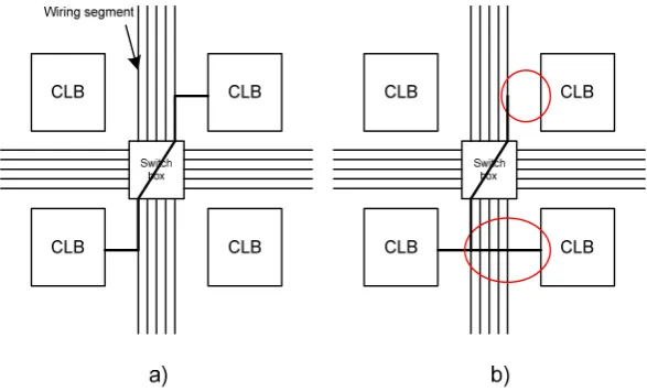
The SEU induced faults in FPGA can manifest in internal memory cells and in FPGA configuration memory. SEU fault in internal memory of the FPGA can corrupt the contents of a block RAM or a flip-flop. Upsets within the configuration memory are especially challenging because these upsets may change the behavior of the FPGA. FPGA configuration is comprised of logic units, which are called Configurable Logic Blocks (CLB) and external routing that connects the CLBs.
The external routing consists of switch boxes and wiring segments shown in Fig. 1a. The connections of
the switch box and the wiring segments are determined by the logic state of their configuration bits. A SEU affecting these configuration bits could disconnect the original CLB connection, or in another case, connect wrong CLBs. For illustration, some typical faults are shown in Fig. 1b (marked by cycle).
The simplified structure of a CLB is shown in Fig. 2. The CLB in Xilinx FPGA consists of a number of look-up tables, flip-flops and internal routing. Candidates for SEU induced faults in a CLB are:
Look-up table bits. A SEU changes the logic function implemented by the look-up table.
Look-up table configuration bits. For example, the bits that determine if a look-up table resource is configured as a look-up table, as a dual port RAM, or as a shift register. A SEU changes the functionality of the look-up table.
Figure 2. Sources of faults in the simplified CLB structure
Row n Row 0
Row 0 Row n
Top 0
Top 1 Major address
k Configuration frame
1312 bits
Minor 0 Minor m
Major address 0
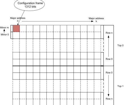
2.2. FPGA configuration memory structure
The FPGA configuration memory determines the functionality of the FPGA organized in a network of configuration frames that are laid out on a device according to their frame address [23], [24]. A frame is the smallest reconfigurable part of FPGA. The size of a frame in Virtex 4 and Virtex 5 FPGA is 41 words of 32-bits. The frame address is comprised of block type (CLBs, BRAM contents, BRAM interconnect), top/bottom bit, row, major address, and minor address. The structure of the FPGA configuration is depictured in Fig. 3.
2.3. SEU risk assessment
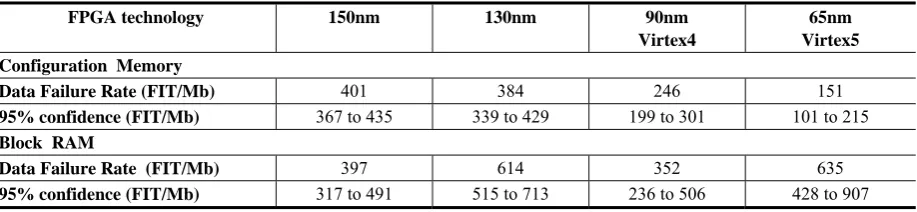
It is known that SEUs are a major factor in the space applications, but there is also a considerable risk of SEU in the atmosphere. The atmospheric SEU risk assessment was made by Xilinx in the Rosetta experiment [13,14]. In the experiment the effect of SEUs on different FPGAs at different altitudes was measured. The SEU error rate is stated in failures in time (FIT) or mean time between failures (MTBF). FIT is the number of failures that can be expected in 109 hours. Table 1 shows the atmospheric test results
for different FPGA technologies. The failure rates of configuration cells do not increase with higher integration densities because additional cell hardening techniques are applied. The configuration cells are
robust based on their requirement to remain static most of the time while block RAM memory must switch between states quickly for operational reasons. This makes them more susceptible to SEUs.
The Rosetta experiment demonstrates that:
in the majority of cases, a SEU only changes (flips) a single bit. Multiple-bit upsets (MBUs) due to a single ionizing particle almost never occur,
there is a high probability that the upset bit in the configuration memory will not affect the functionality of the design because normally less than 10% of the configuration cells are significant to the design implementation,
block RAM memory cells are more susceptible to SEUs then the configuration cells. For this reason Xilinx introduced an ECC option for BRAM in their Virtex 5 FPGA family.
flip-flops are least likely to suffer from a SEU. The flip-flop of Virtex 5 device has approximately 0.06 FIT/Mb that is equivalent to nearly 2 million years of MTBF for the medium sized device. Hence the mitigation strategies of flip-flops are normally omitted.
From the experiment we can conclude that a single error correction strategy against SEUs in the configuration memory and block RAM is a reasonable precaution in practice.
Table 1. Failures in time by FPGA technology
FPGA technology 150nm 130nm 90nm
Virtex4
65nm Virtex5 Configuration Memory
Data Failure Rate (FIT/Mb) 401 384 246 151
95% confidence (FIT/Mb) 367 to 435 339 to 429 199 to 301 101 to 215 Block RAM
Data Failure Rate (FIT/Mb) 397 614 352 635
95% confidence (FIT/Mb) 317 to 491 515 to 713 236 to 506 428 to 907
3. Error-recovery technique for multiprocessor system
Our technique is designed for an embedded multiprocessor SOC on FPGAs. In this arrangement, one of the processor cores scans the configuration frames and performs reconfiguration in the case of detected faults (first pass recovery). If the processor core itself is affected by SEU, another processor core takes the role and performs reconfiguration (extended recovery).
During system normal operation the selected processor core performs a configuration check in parallel with target system application. As stated in the introduction, FPGA circuits are vulnerable to SEU. A fault may occur in any configuration memory cell at any time. Consequently, a processor core which checks the configuration memory is also subject to
SEU induced faults. In order to solve the problem, the processor core always performs a self-test after configuration check. We assume that if the processor core that checks the configuration core is corrupted, it will never report the result of the self-test as fault-free. This is analogous to the asymmetric test invalidation used in the BGM model [2]. Processor self-test can be accomplished in a number of ways, in our implementation we followed the approach proposed in [22].
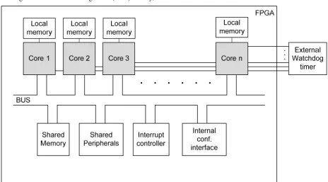
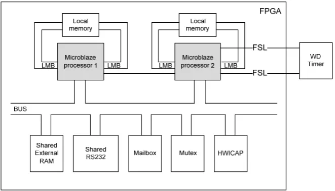
3.1. Required hardware platform
The required hardware infrastructure is depictured in Fig. 4. The hardware requirements are:
a multi-core system with n embedded
an internal partial reconfiguration interface that the processor cores have a common access to,
a mechanism for mutual exclusion to enable one process to gain exclusive access to a particular shared peripheral,
an interrupt controller,
an external watchdog timer.
3.2. Error detection and recovery procedure
Error detection and correction is performed through the peripheral core with internal access to the FPGA configuration memory. In Xilinx FPGAs the Internal Configuration Access Port (ICAP) core is provided. The ICAP core enables an embedded microprocessor to read and write the FPGA configuration memory through the ICAP device at run time, which enables the user to write software programs for an embedded processor that modify the circuit structure and functionality during the circuit operation. Virtex 4 and Virtex 5 FPGA devices include a configuration Error Correcting Code (ECC) facility,
which can be used to detect errors in the configuration frames. The ECC utilizes a Hamming code algorithm that locates single errors and detects double errors. After reading a configuration frame, the output of the ECC produces a syndrome value. For any single error
in the frame, the 11-bit syndrome value identifies an erroneous bit within the frame. Table 2 provides a decomposition of the syndrome value and its corresponding error status.
Table 2. Syndrome value and corresponding error status
Syndrome Bit 11
Syndrome Bit 10 to 0
Error status
S[11]=0 S[10:0]=0 No error S[11]=1 S[10:0]≠0 Single bit error - S[10:0] is
the location of the error S[11]=1 S[10:0]=0 Single bit error overall parity
bit is in error S[11]=0 S[10:0]≠0 Double bit error, not
correctable
Figure 4. The hardware platform architecture
3.3. Error recovery algorithm
A processor on which the configuration readback and error correcting will run is selected. The test algorithm scans through all the configuration frames. It reads and examines the ECC syndrome value of a particular frame and in the case of a fault takes appropriate actions. A fault can manifest in different ways. Possible scenarios of errors and their recovery are:
An error occurs on non-selected processors or other peripherals. The selected processor corrects the fault.
A double error occurs on non-selected processors or other peripherals. The fault can be detected but cannot be corrected. The entire system is reconfigured.
An error stops the selected processor. After time-out, the watchdog timer triggers the next processor which tries to correct the fault.
An error affects the clock routing. The watchdog timer detects the fault. The fault is uncorrectable. The entire system is reconfigured.
An error affects global signals and configuration registers of the FPGA. The watchdog timer detects the fault. The fault is uncorrectable. The entire system is reconfigured.
A hard-error occurs. This error is a permanent failure of the circuit and is not recoverable by reconfiguration. After the single error is detected the recovery the algorithm tries to recover the frame. The frame is checked and if the error still exists the algorithm reports a hard-error.
Recovery algorithm pseudo code
FOR each_frame DO
read_frame(frame_address) read_syndrome()
IF syndrome = single_error THEN locate_error()
h = reconfigure_and_check_frame() IF h = 1
report_hard_error() stop()
ELSE
report_single_error() END IF
ELSE IF syndrome = double_error THEN report_double_error()
stop() ELSE
next_frame() END IF
END FOR
IF self_test() = OK reset_watchdog()
next_processor(processor number++) ELSE
report_selftest_fail() stop()
END IF
3.4. Test scheduling
The test scheduling algorithm can adjust the test period and select the processor core on which the test will run. Shorter test period results in shorter fault detection latency, but decreases available processor resources for the end user. The shortest fault detection latency is achieved if the test runs continuously.
Configuration memory check and recovery runs on one processor while other processors perform user operations. In our implementation, the processor that currently performs the algorithm is selected in a round robin fashion. Other test scheduling strategies are possible at the operation system level.
4. Practical application of error recovery method
The recovery algorithm was studied on a dual MicroBlaze processor design. Both processors have access to external memory. Apart from sharing the external memory, the two processors have their own local memory. Each processor has an interrupt controller assigned to it to handle interrupts. The processors have a common access to the XPS_hwicap
core. This Xilinx core is used for internal access to the configuration. It enables readback of the configuration memory and the partial reconfiguration. The processors use the Xilinx XPS_Mutex core to
synchronize the access to the shared peripherals. The design also has an external hardware watchdog timer connected to the processors through the Fast Symplex Link (FSL). Fig. 5 shows a block diagram of the dual processor system.
The test algorithm runs on one processor at a time and is triggered by interrupts. When a processor finishes the check and self-test correctly it triggers the interrupt on the next processor. If a fault causes the error on the processor and it fails the self-check or stalls during the check, the watchdog timer is not reset in time. It counts down and it triggers an interrupt on the next working processor to correct the fault.
4.1. SEU fault emulation experiment
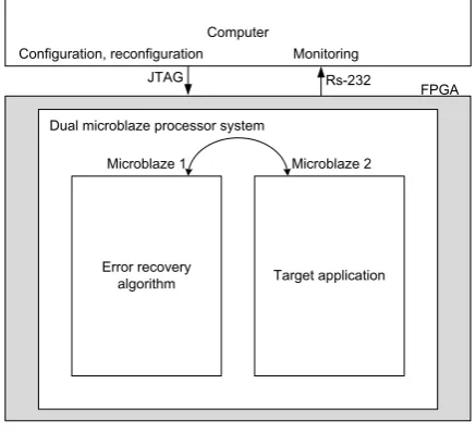
Fault emulation experiment was performed to assess the performance of the error recovery algorithm. Fault emulation was assisted by an external computer. The program on the computer randomly selected the location of the fault and crated “faulty” partial bitstream. Then the altered partial bitstream was sent to the device through the JTAG configuration interface. The system on the FPGA was monitored using the RS-232 serial communication.
For each injected fault, system self-test was performed in order to determine if the injected fault was located in the FPGA configuration memory used for the target application or not. In this particular case, system self-test can be regarded as the actual target application. Next, for the same injected fault the proposed error detection and recovery algorithm was performed in a round robin fashion. If the system on the FPGA had not recovered from the fault, the whole configuration was reconfigured before the next injected fault. The structure of the fault emulation system is shown in Fig. 6. The time period between two injected faults was large enough for the system to finish error recovery and test program on both processors.
Dual microblaze processor system
FPGA
Error recovery
algorithm Target application Microblaze 1 Microblaze 2
Computer Configuration, reconfiguration
JTAG Rs-232
Monitoring
Figure 6. The structure of fault emulation system
4.2. Fault emulation results
Table 3 presents the results of the fault emulation experiment. 5000 random single bit flip faults were injected into the system. 247 of them (i.e., 4.9 %)
affected some critical location and caused a fault in the tested system. 188 out of 247 (i.e., 76 %) were detected and recovered by the error recovery algorithm, while the remaining 59 caused the system to fail. From the 188 recovered faults, 61 faults caused the processor failure on the scrubbing processor and the system was recovered by the other working processor.
Table 3. Fault emulation results
Scenario Faults
All injected random SEU faults 5000 Faults that affected the system 247 System recovered
First pass recovery Extended recovery
188 127 61
System did not recover 59
Obtained fault emulation results were compared to other reported solutions. The techniques described in [9] and [12] use the same principle of error detection and correction. The recovery controller is a single embedded microprocessor (PicoBlaze). The recovery method depends on the correct operation of the processor controller: if a fault causes the processor to fail the system cannot be recovered. Our technique has the advantage that it can adopt itself to another working processor and recover the system. As shown in Table 3, 247 faults affected the system under test. The system has recovered from 127 by the first processor unit (the same techniques as employed in [9], [12]) and from additional 61 faults after switching from a stalled (faulty) processor to another processor.
4.3. Reliability issue
The reliability of the particular device can be calculated by multiplying the estimated nominal SEU failure rate which is stated in failure-in-time per megabyte (FIT/Mb) and the number of critical bits. A
critical bit is any bit that is important for the functionality of the implemented application. In the critical bit analysis we followed the procedures from Xilinx Critical bit report [10].
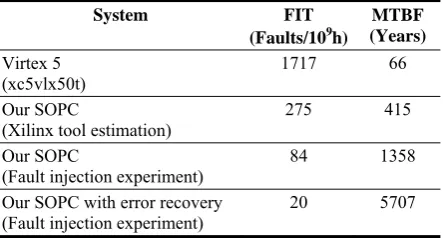
The hardware design of our system was implemented on Virtex 5 xc5vlx50t. According to the Rosetta experiment [13] a Virtex 5 device has a nominal SEU failure rate 151 FIT / Mb.
The reliability estimation of our dual processor system is shown in Table 4. The xc5vlx50t has approximately 11.37 Mb of relevant configuration cells. Therefore this FPGA has a nominal susceptibility of 1717 FIT or a MTBF of approximately 66 years.
FPGA configuration bits were potentially critical to our design. Hence, the maximum susceptibility to SEU of our design is 275 FIT.
The above susceptibility of our design was a worst case estimation. During fault injection experiment we performed system self-test which indicated that 4.9 % of the 5000 random faults affected the functionality of implemented application. Hence, the critical bit count is smaller and the nominal susceptibility of our system without the error recovery algorithm is around 84 FIT. The system with error recovery algorithm has recovered from 76% of these critical faults. Therefore, our SOPC with error detection has a nominal susceptibility to SEU faults of 20 FIT which corresponds to 5707 years between two failures (MTBF).
The above failure rate estimation was done for atmospheric environment using the data from the Xilinx Rosetta experiment. The SEU failure rates in other environments can be much higher. At places with high elevation above the sea, the SEU rates can be three or four times higher than at the sea-level. In an airplane, the SEU effect can be 100-800 times worse than at the sea-level and in the space environment the rates are even higher.
To increase the reliability and dependability the system has to be carefully designed to prevent faults affecting more than one processor core at a time. The processor cores in the FPGA have to be placed in such a way that they are isolated from each other and the internal signals have to be carefully routed to limit the possibility that an upset would affect more than one processor. The reliability design methodology is described in [4].
Table 4. SEU reliability estimation of our dual processor
system
System FIT (Faults/109h)
MTBF (Years)
Virtex 5
(xc5vlx50t) 1717 66
Our SOPC
(Xilinx tool estimation)
275 415
Our SOPC
(Fault injection experiment)
84 1358
Our SOPC with error recovery (Fault injection experiment)
20 5707
5. Conclusions and future work
Highly reliable applications on FPGAs employ SEU mitigation techniques at different system levels. Our approach can be regarded as a low level technique which runs independent of the target application. The salient feature of the proposed approach is low hardware overhead since FPGA configuration memory checking is performed by the same resources as those employed in the target application. Different test scheduling techniques are possible, which provides
confirms the validity of the proposed approach. Currently, the proposed approach is being applied in the design of a new generation of a non-volatile data-storage unit developed for a gaming-system where a very high level of data security and reliability is required. For this purpose, a low area-overhead SEU recovery mechanism based on a finite state machine (FSM) has been developed. In order to assure high reliability TMR structure is employed. Initial fault emulation experiments are showing promising results.
References
[1] H. Asadi, M. B. Tahoori, B. Mullins, D. Kaeli, K. Granlund. Soft Error Susceptibility Analysis of SRAM-Based FPGAs in High-Performance Information Systems. In: Trans. on Nucl. Sci., vol. 54, pp 2714-2726, 2007.
[2] F. Barsi, F. Grandoni, P. Maestrini. A Theory of
Diagnosability of Digital Systems. IEEE Transactions on Computers, vol. C-25, n. 6, pp. 585 – 593, 1976. http://dx.doi.org/10.1109/TC.1976.1674658.
[3] C. Bolchini, A. Miele, M. D. Santambrogio. TMR
and Partial Dynamic Reconfiguration to mitigate SEU faults in FPGAs. In: Proc. Defect and Fault Tolerance in VLSI Systems, 2007, pp. 87-95.
[4] C. Bolchini, A. Miele, C. Sandionigi. A Novel Design
Methodology for Implementing Reliability-Aware Systems on SRAM-Based FPGAs. In: IEEE Transactions on Computers, vol. 60, n. 12, pp 1744-1758, 2011. http://dx.doi.org/10.1109/TC.2010.281.
[5] C. Carmichael. Triple module redundancy design
techniques for Virtex FPGAs. In: Xilinx Corporation, 2001, XAPP197 (v1.0).
[6] C. Carmichael,M. Caffrey, A. Salazar. Correcting single-event upsets through virtex partial configuration. In: Xilinx Corporation, 2000, XAPP216 (vl.0).
[7] C. Carmichael, C. Wei Tseng. Correcting
Single-Event Upsets in Virtex-4 FPGA Configuration Memory. In: Xilinx Corporation, 2009, XAPP1088 (vl.0).
[8] M. Ceschia, A. Paccagnella, S.-C. Lee, C. Wan, M. Bellato, M. Menichelli, A. Papi, A. Kaminski, J. Wyss. Ion beam testing of ALTERA APEX FPGA’s.
In: Proc. NSREC Radiation Effects Data Workshop Record, 2002.
[9] K. Chapman. SEU strategies for Virtex-5 Devices. In: Xilinx Corporation, 2010, XAPP864 (v2.0).
[10] K. Chapman. Virtex 5 SEU Critical Bit Information.
In: Xilinx Corporation, 2010, (v1.0).
[11] E. Fuller, M. Caffrey, P. Blain, C. Carmichael, N. Khalsa, A. Salazar. Radiation test results of the virtex
FPGA and ZBT SRAM for space based reconfigurable computing. In: Proceedings of MAPLD, 1999, p.p. 1-8.
[12] J. Heiner, N. Collins, M. Wirthlin. Fault Tolerant ICAP Controller for High-Reliable Internal Scrubbing. In: Proc. IEEE Aerospace Conf, 2008, p.p. 1-10.
[13] A. Lesea, S. Drimer, J. Fabula, C. Carmichael, P. Alfke. The Rossetta Experiment: Atmospheric Soft
[14] A. Lesea. Continuing Experiments of Atmospheric Neutron Effects on Deep Submicron Integrated Circuits. In: Xilinx Corporation, 2009, WP286 (v1.0.1).
[15] F. Lima Kastensmidt, L. Carro, R. Reis.
Fault-Tolerance Techniques for SRAM-Based FPGAs. First ed., Springer, Dordrecht, 2006.
[16] F. Lima, C. Carmichael, J. Fabula, R. Padovani, R. Reis. A fault injection analysis of Virtex FPGA TMR
design methodology. In: Proc. of the European Conference on Radiation and its Effects on Components and Systems, 2001, p. p. 275 – 282. [17] E. Normand. Correlation of inflight neutron dosimeter
and SEU measurements with atmospheric neutron model. In: IEEE Trans. On Nuclear Science, vol. 48, no. 6, p.p. 1996 - 2003, 2001. http://dx.doi.org/10. 1109/23.983162.
[18] W. Peterson. Error-correcting codes, second ed., Cambridge, The Mit Press, 1980.
[19] B. Randell, P. A. Lee, Philip C. Treleaven.
Reliability Issues in Computing System Design. In: ACM Computing Surveys, vol. 10. n. 2, pp. 123-165, 1978. http://dx.doi.org/10.1145/356725.356729
[20] M. Rebaudengo, M. Sonza Reorda, M. Violante. A new functional fault model for FPGA Application-Orianted testing. In: Proc. Defect and Fault Tolerance in VLSI Systems, 2002, pp. 372 – 380.
[21] S. Rezgui, G.M. Swift, K. Somervill, J. George, C. Carmichael, G. Allen. Complex Upset Mitigation
Applied to a Re-Configurable Embedded Processor. In: IEEE Trans. on Nucl. Sci., vol. 52, n. 6, pp 2468-2474, 2005. http://dx.doi.org/10.1109/TNS.2005.860743
[22] M. Wegrzyn, F. Novak, A. Biasizzo, M. Renovell.
Functional testing of processor cores in FPGA-based applications. In: Computing and Informatics, vol. 28, n 1, pp. 97-113, 2009.
[23] Xilinx. Virtex-4 FPGA Configuration User Guide. In: Xilinx Corporation, 2009, UG071 (v1.11).
[24] Xilinx. Virtex-5 FPGA Configuration User Guide. In:
Xilinx Corporation, 2009, UG191 (v3.8).
[25] C. C. Yui, G. M. Swift, C. Carmichael, R. Koga, J. S. George. SEU Mitigation Testing of Xilinx Virtex II FPGAs. In: Radiation Effects Data Workshop Record, 2003.