Modulation Method For A Dual-Buck Inverter Which
Minimizes Zero Crossing Distortion And Circulating
Current
1
Doddabasappa N* and
2Sanjay Lakshminarayan
1School of EEE, Reva University, Bangalore, India
2School of EEE, Ramaiah Institute of Technology, Bangalore, India
This paper presents a low cost dual buck inverter with high efficiency without any reverse recovery issues for the MOSFET. It is ideal for super junction Power MOSFET application, when used for bipolar PWM in case of PV applications, the duty cycle will be around 50% at zero crossing and there will be distortion of current. As low cost, high reliability, high efficiency and low output distortion of alternating current are very crucial in the design of inverters. This paper proposes a novel method for modulation of bipolar PWM, which will minimize the current distortion at zero crossing and achieves low circulating current. The simulation results validate the method.
Keywords: Inverter, High Efficiency, Zero Crossing Distortion.
INTRODUCTION
With the advances in the renewable sector, there is a large potential for renewable sources like wind solar, PV etc. There is a great growth in PV sector with the intervention of government policies, subsidies for using PV for generation of electricity. There are many products using PV, one of them is the topology without a transformer less to eliminate the 50Hz transformer to achieve high efficiency and low cost. The inverters without a transformer are low cost as they use silicon device and have high efficiency as they have less switches and use super junction Power MOSFETs
The efficiency of the inverter can be improved by many ways, such as by designing a new inverter circuit, by using advanced devices like super junction power MOSFET, SiC devices. These devices are widely used in power factor correction circuits, battery chargers etc because of their low conduction and switching losses. In this paper a dual buck inverter without reverse recovery problem for MOSFETs is introduced and it is also useful for the application in super junction power MOSFET. (S. K. Chowdhury and M. A. Razzak, 2014; Xiangdong Zong, 2011; Frede Blaabjerg et
al., 2004; Zhilei Yao et al., 2009; Soeren Baekhoej Kjaer et al., 2005; Tamas Kerekes et al., 2009).
In case of dual buck PV inverter, bipolar PWM method is used. This is because of the leakage current in transformer less PV inverters. This paper is organized as (A)-Introduction of high reliability and efficiency dual-buck full bridge transformer less inverter. This uses a conventional bipolar PWM method (CB-PWM).
(B)-Introduces an improved bipolar PWM with distortion at zero crossing current, but solves the inverter circulating current and also the leakage current of the PV panel. (IB-PWM) (C)-Takes care of the distortion at zero crossing current, by introducing a novel nonlinear bipolar PWM. (D)-All the inverter topologies are analysed and compared based on the THD values of each topology.
*Corresponding author: Doddabasappa N, School of EEE, Reva University, Bangalore, India. Email: [email protected]
Vol. 3(2), pp. 061-066, November, 2017. © www.premierpublishers.org, ISSN: 3254-1213x
DUAL BUCK INVERTER
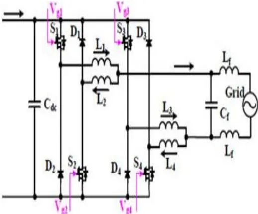
The Fig.1 shows a Dual-buck full-bridge PV inverter. It is very reliable as it will eliminate the reverse recovery problems, dead time and shoot-through. This dual buck full bridge inverter is proposed so that the properties and advantages of power MOSFETs can be utilized. The size of the passive components, resistive nature of the conduction voltage drops, lower switching losses, instant switching speed are all the benefits of power MOSFETs. As seen from Fig.1, it has unidirectional inductor current and works for positive and negative half cycle current. But it has a drawback that four separate inductors are required. (B. F. Chen, 2012; Henry Benedict Massawe et al., 2013; Zhilei Yao et al., 2009; Ahmed Abdalrahman et al., 2012; S. K. Chowdhury and M. A. Razzak, 2013; Marco Liserre et al., 2005).
Fig.1: High efficiency transformer-less dual-buck full bridge PV inverter
SIMULATION AND RESULTS
A-TRADITIONAL BIPOLAR PWM METHOD
The block diagram of the conventional bipolar PWM (CB-PWM) is shown in Fig.2.In order that the proposed dual buck full bridge inverter must adopt to the CB-PWM for applications of PV,the dual to common mode voltage from CB-PWM is always fixed to Vdc/2.
Fig. 2: Conventional bipolar PWM (CB-PWM) method Fig. 3(a) and 3(b) show the operating mode and equivalent circuit for the CB-PWM when switches S1 and S4 are turned ON and when switches S2 and S3 are turned ON respectively.
When S1 and S4 are conducting, freewheeling current of L2 and L3 would circle back to DC bus through D1 and D4. Similarly, When S2 and S3 are conducting, freewheeling current of L1 and L4 flow back to DC bus through D2 and D3, it leads to a circulating current and decrease efficiency. The simulation results for dual buck inverter using CB-PWM are shown in Fig.4 without filter. The highlighted circle in the waveform indicates the presence of circulating current in the negative half cycle.
Fig. 3(a): Operating mode and equivalent circuit during S1 and S4 turn on.
Fig. 4: Simulation results with CB-PWM method without Filter
B. IMPROVED BIPOLAR PWM METHOD
The improved bipolar PWM (IB-PWM) is shown in Fig.5.Here the current polarity is taken into consideration (Frede Blaabjerg et al., 2004; Zhilei Yao et al., 2005; Soeren Baekhoej Kjaer et al., 2005) and each inductor operates under both positive and negative half cycle currents. Hence PWM is fed to the switches considering the polarity.
Fig. 5: Improved bipolar PWM (IB-PWM) method
The Fig.6 (a),6 (b), 6(c), 6 (d) all show the operating model and equivalent circuits for the IB-PWM .During the positive half cycle, the switches S1 and S4 will be switching and the freewheeling current will pass through D2 and D3. During the negative half cycle, the switches S2 and S3 will be switching and the freewheeling current will pass through D1 and D4.
The simulation results for IB-PWM are shown in Fig.7.We see that the circulating current is eliminated and switching power loss is also reduced. But, the current in zero-crossing region would have an obvious distortion, which originates from the discontinuous-conduction mode (DCM) condition.
Fig.6 (a) Charging Interval during Positive Half Cycle
Fig.6 (b) Freewheeling Interval during Positive Half Cycle
Fig.6 (c) Charging Interval during Negative Half Cycle
Fig. 7: Simulation results with IB-PWM method The Volt-second balance equation on inductor is,
When inductor current is under continuous-conduction mode (CCM) condition, TB-PWM method and IB-PWM method have same Volt-second balance equation, which is [5],
(2) However, during DCM condition at unity PF operation, The Volt-second equation for IB-PWM method will be
So, if Vref = 0, switching on & off time would be:
(4)
And ripple current & average current would be:
(5)
Assume Vref & output current Iac are in the phase, when current is positive and S1-S4 are conducting, the relationship between the duty cycle (D) and Vref is:
When Vre = 0, D will be 50%, it will let current in boundary mode [ibm] which depends on current ripple.
When current is negative and S2-S3 are conducting, the relationship between the duty cycle (D) and Vref is:
When Vref = 0, D will be 50%, it will let current in boundary mode [-ibm ] which depends on the current ripple.
The current changes from +ibm and –ibm at the zero crossing over of the current, the duty cycle will be 50%. Due to the distortions at the zero crossing over the THD of the output AC current is 29.66%. These simulation results are shown in Fig.7.
C. NOVEL PWM MODULATION METHOD FOR CURRENT ZERO-CROSSING
The proposed method combines the advantages of both CB-PWM without distortion and IB-PWM with high efficiency. The Fig.8 shows the proposed method, which uses the unipolar method.
Fig. 8: Proposed Novel PWM Modulation Method in Dual Buck Inverter
In this paper a new modulation method is proposed to provide a duty cycle of 0% at zero cross over. This in turn makes the inductor current to enter DCM instead of boundary mode.
Fig. 9: Simulation Results with Proposed Bipolar PWM Method in Dual Buck Inverter
THD ANALYSIS AND COMPARISON FOR ALL THE INVERTER TOPOLOGIES
THD calculations can be obtained from SIMULINK. The switching pattern that is used in this project for all the inverters topologies are harmonic elimination method.
Where,
V1= Fundamental Voltage magnitude V2 = Magnitude of 2nd Harmonic V3 = Magnitude of 3rd Harmonic V4 = Magnitude of 4th Harmonic Vn = Magnitude of nth Harmonic
TABLE 1: Total Harmonic Distortion Analysis
METHODS TOTAL HARMONIC DISTORTION IB-PWM 29.66%
NOVEL-PWM 3.77%
Fig.10: THD comparison between Novel PWM method And IB-PWM method
CONCLUSION
Nowadays the inverters are without transformers with high efficiency and less cost. This paper introduces a dual buck inverter to reduce the distortion and circulation current at zero cross over.
Detail discussion and analysis point out:
• In case of Traditional bipolar PWM technique, there will be circulating current and current distortion will not be present.
• With the Improved bipolar PWM technique, there will be no circulating current, but significant current distortion will be present.
REFERENCES
Ahmed Abdalrahman, Abdalhalim Zekry, and Ahmed Alshazly (2012). Simulation and Implementation of Grid-connected Inverters”, International Journal of ComputerApplications (0975 – 8887) Volume 60– No.4. Chen BF, Sun PW, Liu C, Chen C-L., Lai J.-S., and Yu W. (2012). High efficiency transformerless photovoltaic inverter with wide-range power factor capability. Proc. of IEEE Applied Power Electronics Conference and Exposition, Orlando, FL.
Chowdhury SK and Razzak MA. (2013). A Combined π- and T-type Immittance Converter for Constant Current Applications. Proceedings of the IEEE International Conference on Informatics, Electronics & Vision (ICIEV), Dhaka Bangladesh.
Chowdhury SK and Razzak MA. (2014). Design of a Transformer-less Grid-Tie Inverter Using Dual-Stage Buck and Boost Converters. International Journal Of Renewable Energy Research., Vol.4, No.1.
Frede Blaabjerg, Zhe Chen and Soeren Baekhoej Kjaer (2004). Power Electronics as Efficient Interface in Dispersed Power Generation Systems. IEEE Transactions On Power Electronics, VOL. 19, NO. 5. Henry Benedict Massawe, Lars Einar Norum, Elkraft
(2013). Grid Connected Photovoltaic Systems with SmartGrid functionality. Master of Science in Electric Power Engineering Department of Electric Power Engineering. Norwegian University of Science and Technology.
Marco Liserre, Frede Blaabjerg, Steffan Hansen (2005). Design and Control of an LCL Filter-Based Three-Phase Active Rectifier. IEEE Transactions on Industry Applications, pp.VOL. 41, NO. 5.
Mohan N., Undeland T. M., and Robbins W. (2006). Power Electronics, 3rd Ed.,Denvers, MA: John Wiley & Sons, Inc., pp. 211-214.
Rashid MH. (2007). Power Electronics, Circuits, Devices, and Applications, 3rd Ed. New Delhi: Prentice-Hall of India Private Limited. pp.253-256.
Tamas Kerekes , Remus Teodorescu , Marco Liserre Christian Klumpner and Mark Sumner (2009). Evaluation of Three-Phase Transformerless Photovoltaic Inverter Topologies. IEEE Transactions On Industry Applications, VOL.24, NO.9.
Texas Instruments Incorporated (2012). Basic Calculation of a Buck Converter's Power Stage. SLVA477A– December 2011–Revised August 2012, Copyright © 2011–2012.
Xiangdong Zong (2011). A Single Phase Grid Connected DC/AC Inverter with Reactive Power Control for Residential PV Application. A thesis submitted in conformity with the requirements for the degree of Masters of Applied Science, Graduate Department of Electrical and Computer Engineering,University of Toronto.
Zhilei Yao, Lan Xiao and Yangguang Yan (2009). Dual-Buck Full-Bridge Inverter With Hysteresis Current Control” IEEE Transactions On Industrial Electronics, VOL. 56, NO. 8.
Zhilei Yao, Lan Xiao, Member IEEE, and Yangguang Yan (2009). Control Strategy for Series and Parallel Output Dual-Buck Half Bridge Inverters Based on DSP Control. IEEE Transactions On Industry Applications,VOL. 24, NO. 2.
Accepted 23 October, 2017
Citation: Doddabasappa N and Lakshminarayan S (2017). Study H and Estimation of Energy Transfer to the Active DC-Link Capacitor Due to Harmonic Current. International Research Journal of Power and Energy Engineering, 3(2): 061-066.