Ames Laboratory Accepted Manuscripts Ames Laboratory
2018
Extracting interface locations in multilayer polymer
waveguide films using scanning angle Raman
spectroscopy
Jonathan M. BobbittIowa State University and Ames Laboratory
Emily A. Smith
Iowa State University and Ames Laboratory, [email protected]
Follow this and additional works at:https://lib.dr.iastate.edu/ameslab_manuscripts
Part of theMaterials Chemistry Commons, and thePolymer and Organic Materials Commons
This Article is brought to you for free and open access by the Ames Laboratory at Iowa State University Digital Repository. It has been accepted for inclusion in Ames Laboratory Accepted Manuscripts by an authorized administrator of Iowa State University Digital Repository. For more information, please [email protected].
Recommended Citation
Bobbitt, Jonathan M. and Smith, Emily A., "Extracting interface locations in multilayer polymer waveguide films using scanning angle Raman spectroscopy" (2018).Ames Laboratory Accepted Manuscripts. 68.
Extracting interface locations in multilayer polymer waveguide films using
scanning angle Raman spectroscopy
Abstract
There is an increasing demand for nondestructive in situ techniques that measure chemical content, total thickness, and interface locations for multilayer polymer films, and scanning angle (SA) Raman spectroscopy in combination with appropriate data models can provide this information. A SA Raman spectroscopy method was developed to measure the chemical composition of multilayer polymer waveguide films and to extract the location of buried interfaces between polymer layers with 7- to 80-nm axial spatial resolution. The SA Raman method acquires Raman spectra as the incident angle of light upon a prism-coupled thin film is scanned. Six multilayer films consisting of poly(methyl methacrylate)/polystyrene or poly(methyl methacrylate)/polystyrene/poly(methyl methacrylate) were prepared with total thicknesses ranging from 330 to 1,260 nm. The interface locations were varied by altering the individual layer thicknesses between 140 and 680 nm. The Raman amplitude ratio of the 1,605-cm−1 peak for polystyrene and 812-cm−1 peak for poly(methyl methacrylate) was used in calculations of the electric field intensity within the polymer layers to model the SA Raman data and extract the total thickness and interface locations. There is an average 8% and 7% difference in the measured thickness between the SA Raman and profilometry measurements for bilayer and trilayer films, respectively.
Keywords
bilayer and trilayer polymer films, polymer–polymer interface, thin-film analysis, vibrational spectroscopy
Disciplines
Materials Chemistry | Materials Science and Engineering | Polymer and Organic Materials
1
Extracting Interface Locations in Multilayer Polymer Waveguide Films using Scanning
Angle Raman Spectroscopy
Jonathan M. Bobbitt and Emily A. Smith*
The Ames Laboratory, U.S. Department of Energy, and Department of Chemistry, Iowa State
University, Ames, IA 50011, United States
Corresponding Author: *Email: [email protected]
Abstract
There is an increasing demand for nondestructive in situ techniques that measure
chemical content, total thickness, and interface locations for multilayer polymer films, and SA
Raman spectroscopy in combination with appropriate data models can provide this information.
A scanning angle (SA) Raman spectroscopy method was developed to measure the chemical
composition of multilayer polymer waveguide films and to extract the location of buried
interfaces between polymer layers with 7–80-nm axial spatial resolution. The SA Raman method
measures Raman spectra as the incident angle of light upon a prism-coupled thin film is scanned.
Six multilayer films consisting of poly(methyl methacrylate)/polystyrene or poly(methyl
methacrylate)/polystyrene/poly(methyl methacrylate) were prepared with total thicknesses
ranging from 330-1260 nm. The interface locations were varied by altering the individual layer
2
812 cm-1 peak for PMMA was used in calculations of the electric field intensity within the
polymer layers to model the SA Raman data and extract the total thickness and interface
locations. There is an average 8% and 7% difference in the measured thickness between the SA
Raman and profilometry measurements for bilayer and trilayer films, respectively.
Keywords: Vibrational spectroscopy, Thin film analysis, Polymer polymer interface, Bilayer
and trilayer polymer films
Introduction
Polymer-polymer interface characterization in multilayer polymer films is important for
their increasing use in energy storage and capture devices,[1-11] coatings and optics,[12-15] food
packaging,[16-18] and biomedical applications.[19] Work on understanding polymer-polymer
interface surface mixing,[20] roughness,[21] and stability[22,23] is a focus of many multilayer
polymer film studies. As important is characterizing the chemical composition, thickness, and
interface locations when creating and optimizing new multilayer polymer devices. Optical-based
spectroscopies are well suited for in situ nondestructive measurements of polymer films.
Infrared variable angle spectroscopic ellipsometry (IR-VASE) is a technique that is
capable of providing multilayer polymer interface and chemical content information.[24] Good
signal-to-noise ratio IR-VASE spectra require 8-12 hour collection times for a single multilayer
polymer film, which limits the real-time analysis of samples. Infrared spectroscopy operated in
attenuated total reflection mode is well suited for monitoring chemical content information
3
thicknesses and buried interface locations from the spectra, however, is complicated due to the
penetration depth of evanescent waves varying across the infrared spectrum.
Raman spectroscopy provides chemical content information using a single excitation
wavelength. Micro-Raman spectroscopy with epi-illumination can provide chemical content
information for thin multilayer polymer films, but does not provide buried interface locations
from polymer films under approximately 2 µm.[28-30] Scanning angle (SA) Raman spectroscopy
is a technique that couples a sample to a prism (a schematic is shown in the top of Fig. 1), and a
data set consist of the Raman spectra as a function of the incident angle of the excitation light.
SA Raman spectroscopy has been used to measure polymer waveguide thicknesses, buried
bilayer film interfaces, and mixed polymer film chemical composition.[31-34] Other reported
methods that are similar to SA Raman spectroscopy, variable-angle internal-reflection and
attenuated total reflection Raman spectroscopy, have been used to measure bilayer polymer
films.[35,36] These studies focused on micron to hundreds of microns thick bilayer films, the
reported methods cannot be easily applied to other polymer systems or, in the work by Fumihiko
et al., no buried interface location was extracted.
Summarized here is a nondestructive method that combines SA Raman spectroscopy and
electric field calculations to extract total thickness and interface locations for thin bilayer and
trilayer polymer waveguide films. Polymer films behave as a waveguide when the thickness is
greater than approximately 𝜆𝜆
2𝜂𝜂, where 𝜆𝜆 is the excitation wavelength and 𝜂𝜂 is the refractive index
of the polymer at the excitation wavelength. When light is coupled into the waveguide through a
prism, constructive interference occurs at discrete incident angles (referred to as waveguide
mode angles), which produces an enhancement in the Raman signal collected at these angles.
4
homopolymer waveguides of varying thicknesses.[31] Raman scattering is proportional to the
square of the electric field, so SA Raman spectra are modeled by plotting the square of the
electric field intensity integrated over the thickness of each polymer layer (i.e., SSEF) as a
function of the incident angle. The current work expands the bilayer polymer film work reported
by Damin et al.[33] in two important ways. First, we apply the SA Raman amplitude ratio
between peaks for each polymer in the film, which has been previously proposed by us to
measure mixed polymer films,[34] and recursive SSEF calculations to reduce the computational
time required to model the SA Raman data. Second, total film thickness and interface locations
for bilayer and trilayer polymer films with distinctly different indices of refraction are reported.
This new method significantly reduces analysis time and is demonstrated on thin (< 1.3 µm)
bilayer poly(methyl methacrylate)/polystyrene (PMMA/PS) and trilayer (PMMA/PS/PMMA)
waveguide films with one or two buried interfaces, respectively. The presented method should be
applicable to measure numerous polymer multilayer films whenever the layers have at least one
distinct Raman peak.
Experimental
Sample preparation
A 31.3 mg/mL PS (192,000 g/mol, Sigma Aldrich, St. Louis, MO), 39.0 mg/mL PMMA
(120,000 g/mol, Sigma Aldrich, St. Louis, MO), 55.3 mg/mL PMMA, and 67.9 mg/mL PMMA
solutions were prepared from 120 mg/mL stock solutions in toluene (Fisher Scientific, Waltham,
MA). The PMMA solutions of varying concentration were used to fabricate PMMA layers with
5
PMMA films were prepared by spin coating 200 µL of solution with a KW-4A spin coater
(Chemat Technology, Northridge, CA) at 3000 rpm for 60 seconds. Glass cover slips (25 mm2
area, Corning Inc., Corning, NY) and sapphire disks (507 mm2 area, Meller Optics, Providence,
RI) were used as substrates, and the film's total and individual layer thicknesses were measured
on an AlphaStep® D-600 stylus profiler (KLA Tencor, Milpitas, CA).
Multilayer films were prepared by using the wedge transfer method.[37] A PS film was
lifted off of the sapphire disk and floated at the water-air interface using a beaker of water. The
PS film was deposited over a PMMA film and the bilayer was dried at 70 °C for 10 minutes. The
bilayer film was then left in a petri dish for 24 hours at room temperature to ensure all the
residual water had evaporated. After the PMMA/PS bilayer SA Raman measurements were
completed, a second PMMA film was lifted off a sapphire disk using a beaker of water and the
second PMMA film was placed on top of the bilayer film to create a PMMA/PS/PMMA trilayer
film. The drying process was repeated for the trilayer samples.
Scanning angle Raman measurements
A home-built instrument, previously reported by Lesoine et al., was used to collect SA
Raman spectra.[38] A 532-nm excitation source (Coherent, Santa Clara, CA) set to s-polarized
light was directed onto a sapphire prism (ISP Optics, Irvington, NY) by coupling the source into
a polarization maintaining single mode fiber (Thorlabs, Newton, NJ). The incident angle was
controlled by using a rotational stage (Zaber Technologies, Vancouver, British Columbia,
Canada), which had the fiber mounted on it with a 28-mW laser output. The SA Raman data
were collected over an angle range of 48.0-62.0° with a 0.2° step size. A 0.25 numerical aperture
10× microscope objective (Leica, Wetzlar, Germany) was used to direct the collected SA Raman
6
HoloSpec ƒ/1.8i spectrograph (Kaiser Optical Systems, Ann Arbor, MI) that was attached to the
side port of the optical microscope. A Newton 940 charged coupled device (Andor Technology,
Belfast, UK) with 2048 × 512 pixels was used to collect the SA Raman spectra for 60s with two
replicate measurements at each angle.
Igor Pro 6.36 scientific analysis and graphing software was used to process all SA Raman
spectra. A Gaussian function with a linear baseline was used to batch fit and extract the
amplitudes of PS and PMMA peaks at 1605 and 812 cm-1, respectively. SA Raman spectra were
plotted as a function of their incident angle using Matlab 2016b. The SA Raman amplitude ratio
(𝑟𝑟𝑃𝑃𝑃𝑃) was calculated at each incident angle using equation 1, where I represents the peak
amplitude at the designated wavenumber for the indicated polymer and 𝜎𝜎𝑅𝑅 is the relative Raman
cross-section (defined in equation 2).
𝑟𝑟𝑃𝑃𝑃𝑃 = 𝐼𝐼𝑃𝑃𝑃𝑃,.1605𝑐𝑐𝑐𝑐
−1
𝐼𝐼𝑃𝑃𝑃𝑃,1605𝑐𝑐𝑐𝑐−1+ (𝐼𝐼𝑃𝑃𝑃𝑃𝑃𝑃𝑃𝑃,812𝑐𝑐𝑐𝑐−1 × 𝜎𝜎𝑅𝑅) (1)
𝜎𝜎𝑅𝑅 = 𝐼𝐼𝑃𝑃𝑃𝑃,1605𝑐𝑐𝑐𝑐
−1
𝐼𝐼𝑃𝑃𝑃𝑃𝑃𝑃𝑃𝑃,812𝑐𝑐𝑐𝑐−1 = 1.0 (2)
The relative Raman cross-section (𝜎𝜎𝑅𝑅) was determined using epi-illumination with a
532-nm excitation source on a XploRA Plus confocal Raman microscope (Horiba Scientific, Edison,
NJ). The samples used to determine 𝜎𝜎𝑅𝑅 were prepared and characterized as previously
reported.[34] The thickness of the samples ensured that the Raman signal was independent of the
optical focus (i.e., the same amount of polymer was measured regardless of the focus). Spectra
were acquired for 5s with 2 accumulations from 3 separate locations.
7
Electric field intensity calculations were performed using finite-difference time-domain
simulations (EM Explorer, San Francisco, CA). The refractive indices of each polymer layer and
the SA Raman amplitude ratio (𝑟𝑟𝑃𝑃𝑃𝑃) were input parameters needed in the calculation to find the
thickness of each layer. The refractive index for 532-nm and s-polarized light was 1.764 for
sapphire, 1.495 for PMMA, and 1.598 for PS.[39-41] A recursive script (included in the
supplemental information) for the finite-difference time-domain calculations varied the total
thickness (10-nm step size) over the range shown in Table 1. For a given total thickness, the
fractional composition of each polymer was modeled by the SA Raman amplitude ratio (𝑟𝑟𝑃𝑃𝑃𝑃),
which was varied in increments of 0.05 over the range of values listed in Table 1. (The range of
values in Table 1 represent the experimentally measured range across all incident angles). While
the SA Raman amplitude ratio does not match the film composition, as discussed below, over the
waveguide mode angle range it can be used to approximate the composition and minimize the
computation time required to fit the data. Because the SA Raman amplitude ratio (𝑟𝑟𝑃𝑃𝑃𝑃) range
varied for each sample (Table 1), the step size for the thickness of each layer also varied with
each sample.
The electric field intensity was calculated over an incident angle range of 48.0-62.0° with
a 0.2° step size unless otherwise noted. A 12-nm Yee cell size was used for all calculations. The
SSEF was determined by integrating the electric field intensity across the entire thickness of the
individual polymer layers. The standard error of the estimate (𝑠𝑠𝑒𝑒𝑒𝑒𝑒𝑒), the square root of the
average across all angles squared deviation of the experimental data from the SSEF fit, was
calculated for each SSEF fit. The lowest 𝑠𝑠𝑒𝑒𝑒𝑒𝑒𝑒 value provided the best fit between the
experimental data and the SSEF fit. For each polymer film, a SSEF fit was individually
8
location(s). Then the average of the PS and PMMA values were calculated. The reported
uncertainties in the total thickness and interface location(s) were determined by finding the
second-best SSEF fit (the second lowest 𝑠𝑠𝑒𝑒𝑒𝑒𝑒𝑒) that is shifted by at least 0.2°, the angular
resolution for these measurements, from the best fit to the experimental data. The waveguide
mode maximum angle for PS and PMMA was determined by fitting the SSEF fit to a Lorentzian
function and the standard deviation was determined from the Igor Pro fitting software.
Results and Discussion
Motivation for determining buried interfaces using SA Raman spectroscopy
Understanding how the electric field varies across the thickness of a bilayer or trilayer
film, as well as with incident angle, is important for understanding the collected SA Raman
signal since the electric field intensity is proportional to the Raman signal. The measured
parameters in the SA Raman data (e.g., peak intensities and waveguide mode angles) in
combination with electric field calculations are used to extract interface locations from thin
bilayer and trilayer polymer waveguide films.
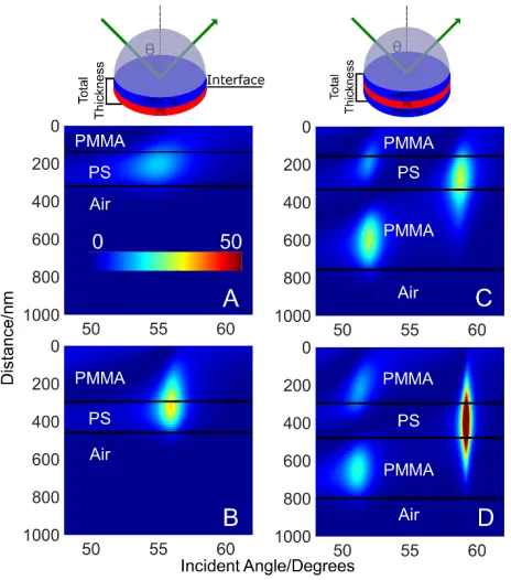
The graph of the electric field intensity across the polymer samples are shown in Fig. 1
for selected bilayer (left) and trilayer (right) films. Hereafter, samples will be referred to with a
sample number (1, 2, or 3) and -Bi (for bilayer) or -Tri (for trilayer) films. The electric field
profiles shown in Fig. 1 are calculated using the experimentally measured polymer thicknesses
for four samples: 1-Bi (Fig. 1A), 2-Bi (Fig. 1B), 1-Tri (Fig. 1C), and 2-Tri (Fig. 1D). All bilayer
and trilayer samples are thick enough (≥167 nm) to behave as a waveguide using 532-nm
9
has 140 nm of PMMA and 180 nm of PS. Across the angle range of 48.0-62.0° a single
waveguide mode is evident, and the waveguide mode angles are at 54.90° and 55.50° for PS and
PMMA, respectively. The electric field intensity is generated in both the PMMA and PS layers.
However, the electric field intensity distribution varies with the incident angle and does not
match the 55% PS polymer composition at all incident angles. For example, 63% of the total
[image:11.612.191.423.245.508.2]electric field intensity is generated in the PS layer at the 54.90° PS waveguide mode angle.
Figure 1: Calculated electric field intensity (square of the electric field) plots as a function of
incident angle and distance from the prism/sample interface, which is located at 0 nm. The color
scale represents the electric field intensity, and the scale in (A) is the same for all plots. The solid
black lines indicate the interface between the polymer layers. The plots show where the electric
field intensity is generated within the polymer films as well as waveguide mode angles. (A)
Sample 1-Bi: 140 nm PMMA, 180 nm PS; and (B) sample 2-Bi: 296 nm PMMA, 159 nm PS.
10
from the prism); and (D) Sample 2-Tri: 300 nm top PMMA, 310 nm bottom PMMA. The
Sample 1-Tri and 2-Tri PS layer thickness is 180 nm. The calculations used a 0.05° step size.
Compared to sample 1-Bi, sample 2-Bi (Fig. 1B) shows an increase in the waveguide
mode angle as the PMMA thickness increases to 296 nm and the PS layer thickness decreases to
159 nm. For both the PS and PMMA layers the waveguide mode angle occurs at 55.95°. With
the increasing PMMA thickness for sample 2-Bi, there is a decrease in the electric field intensity
generated in the PS layer down to 55% compared to the 63% generated in the PS layer for
sample 1-Bi.
For the trilayer films shown in Fig. 1C and D, the PS thickness is constant at 180 nm. The
total thickness is 770 (1-Tri) and 790 nm (2-Tri). Effectively, the PS layer is farther from the
prism interface for sample 2-Tri as the thickness increases for the PMMA layer adjacent to the
prism. The trilayer films are thick enough to generate two waveguide modes within this angle
range, and they are termed mode zero (at high angles) and mode one (at low angles) as observed
in Fig. 1C and D. Fig. S1 (Supporting Information) shows the plots of the calculated electric
field intensity as a function of the distance from the prism/sample interface at the PMMA
waveguide mode angle for sample 1-Tri, where the purple curve is waveguide mode one (51.95°
incident angle) and the orange curve is waveguide mode zero (58.75° incident angle). Similar
plots are obtained at the PS waveguide mode angle. The graphs show that the distribution of the
electric field intensity among the polymer layers varies with each waveguide mode.
In sample 1-Tri waveguide mode zero appears at 58.75° for both PS and PMMA layers,
11
sample 2-Tri waveguide mode zero for PS and PMMA shifts to a higher angle (59.15°), and
waveguide mode one for PS and PMMA decreases by 0.95° and 0.85°, respectively. As the PS
layer moves further away from the prism interface for sample 2-Tri, there is an 8% increase in
the electric field intensity within the PS layer at waveguide mode zero, while there is a 1.5%
decrease at waveguide mode one. Similar trends are observed for sample 3-Bi (Fig. S2A
(Supporting Information)) and sample 3-Tri (Fig. S3A (Supporting Information)). These
representative calculated results suggest it should be feasible to use SA Raman spectroscopy,
with a signal that is proportional to the electric field intensity,[31-34,38,42-45] to measure total film
thickness as well as the location of polymer interfaces for both bilayer and trilayer films.
Development of a SA Raman method with iterative fitting for analyzing bilayer polymer
films
Fig. 2A shows the SA Raman spectra plotted over an incident angle range of 50.0-60.0°
for sample 1-Bi, and Fig. 2B shows a plot of the peak amplitude as a function of incident angle
for the PS (1001 cm-1, red circles) and PMMA (812 cm-1, blue circles) peaks. A single broad
waveguide mode is measured for PS and PMMA, with waveguide mode angles at 54.86 ± 0.02°
for PS and 55.58 ± 0.03° for PMMA. The PMMA amplitude at 812 cm-1 is 2.1× lower compared
to the PS amplitude at 1605 cm-1, which is not due to differences in their Raman cross-section
(𝜎𝜎𝑅𝑅 = 1.0) or the amount of PMMA in the film (there is only 1.2× less PMMA compared to PS
in the sample). Rather, there is an enhancement in the PS signal in sample 1-Bi with the
amplitude being 69% of the total signal collected. This is in agreement with the 63% value from
the electric field calculations. Overall, the waveguide mode angles and peak amplitudes follow
12
Figure 2: (A and C) SA Raman spectra of PMMA/PS bilayer films plotted on the same color
scale shown in A. The color scale represents the SA Raman scattering intensity (Arbitr. Units).
(B and D) show plots of the 1605 cm-1 PS and the 812 cm-1 PMMA peak amplitudes as a
function of the incident angle. The black lines represent the best SSEF fit to the experimental
data. (A and B) correspond to sample 1-Bi and (C and D) correspond to sample 2-Bi.
SA Raman data for sample 2-Bi (Fig. 2C and D) and 3-Bi (Fig. S2B (Supporting
Information)) show the effects of increasing the total thickness. Compared to sample 1-Bi, the PS
and PMMA waveguide modes shift to higher angles. The peak amplitudes increase for sample
2-Bi and 3-2-Bi, and there is an overall decreasing trend in the magnitude of the SA Raman
amplitude ratio (𝑟𝑟𝑃𝑃𝑃𝑃) as the PMMA layer thickness increases (Table 1). The SA Raman data are
[image:14.612.189.424.75.311.2]13
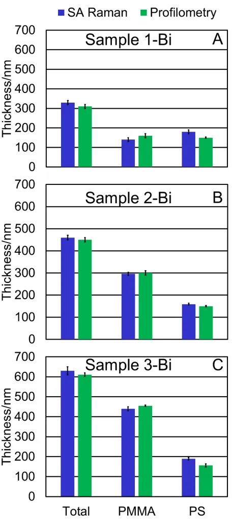
Fig. 3 shows the thicknesses measured for each of the bilayer films by SA Raman
spectroscopy and by profilometry. Overall, the SA Raman measurements properly capture the
increasing PMMA layer thickness, and statistically similar PS thickness for these samples. The
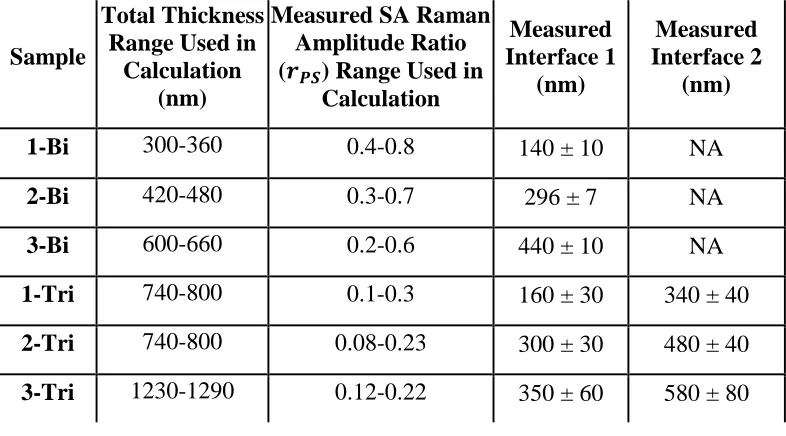
interface locations determined by SA Raman spectroscopy (Table 1) are 140 ± 10 (sample 1-Bi),
296 ± 7 (sample 2-Bi), and 440 ± 10 nm (sample 3-Bi). The total thickness and PMMA layer
thickness determined by the SA Raman method have an average 4% and 6% difference,
respectively, compared to values measured by profilometry. The PS layer thickness has a larger
14% difference compared to the values measured by profilometry. The 𝑠𝑠𝑒𝑒𝑒𝑒𝑒𝑒 is used to
quantitatively determine how well the SSEF calculations fit the experimental SA Raman data.
For sample 1-Bi the 𝑠𝑠𝑒𝑒𝑒𝑒𝑒𝑒 for the best fit to the PS and PMMA data are determined to be 0.043
and 0.052, respectively. The 𝑠𝑠𝑒𝑒𝑒𝑒𝑒𝑒 of the second-best fit that is shifted by at least 0.2° (the angular
resolution of the experimental data) increases to 0.057 and 0.073 (33% and 40% increase) when
the total, PS, and PMMA layer thicknesses change by 10 nm as shown in Fig. S4 (Supporting
Information). Increasing the angular resolution used to collect the experimental data and/or
reducing the thickness increments used in the iterative calculations should improve the average
percent difference between the SA Raman method and profilometry measurements at the cost of
increased instrumental and computational time. It is also important to note that the samples
measured by profilometry are not the same as those measured by the SA Raman method since
profilometry is destructive and can only measure the individual layers prior to forming the
14
Figure 3: (A) Sample 1-Bi, (B) sample 2-Bi, and (C) sample 3-Bi thicknesses measured by the
SA Raman method and profilometry. The profilometry measurements are performed on separate
films fabricated with the same method used to prepare the samples measured by SA Raman
[image:16.612.194.423.73.591.2]15
bilayer are retained in the bilayer. The error bars represent the difference between the best fit and
the second-best fit that is shifted by at least 0.2° for two replicate measurements (SA Raman) and
the standard deviation from three replicate measurements (profilometry).
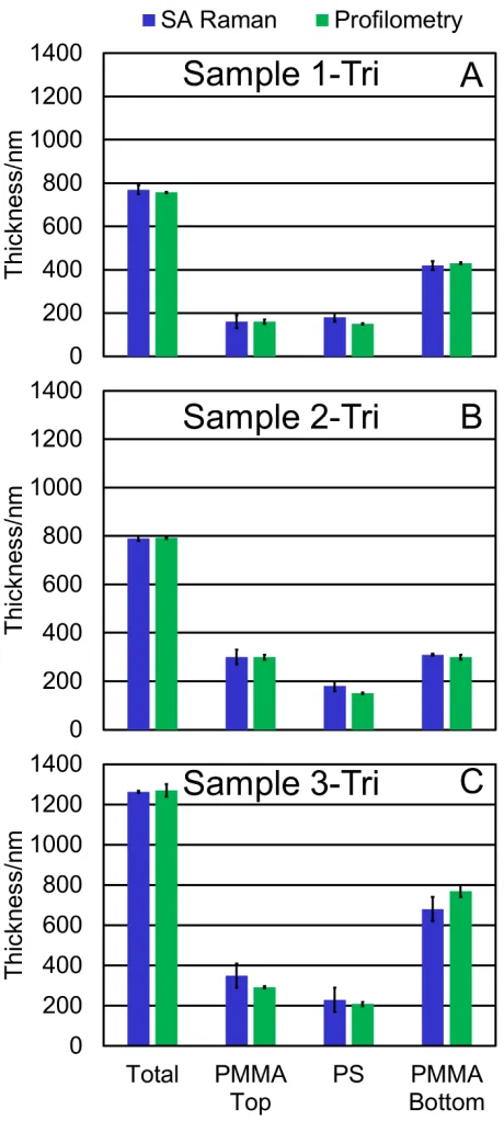
Applying the SA Raman method for analysis of trilayer films
Trilayer films are prepared by transferring a third PMMA layer onto samples 1-Bi and
2-Bi. The corresponding multilayer films are samples 1-Tri and 2-Tri, and their SA Raman spectra
are plotted in Fig. 4A and C. The SA Raman spectra for the trilayer films show similar trends to
the electric field intensity plots (Fig. 1C and D). Waveguide mode one shifts by 0.9° to lower
angles for both PS and PMMA in sample 2-Tri (Fig. 4D) when the PS layer moves farther from
the sapphire prism interface. Data for a third trilayer sample (3-Tri) are shown in Fig. S3
16
Figure 4: (A and C) SA Raman spectra of PMMA/PS/PMMA trilayer films plotted on the same
color scale shown in A. The color scale represents the SA Raman scattering intensity (counts).
(B and D) show the plots of waveguide mode one for 1605 cm-1 PS and the 812 cm-1 PMMA
peak amplitudes versus incident angle. The black lines represent the best SSEF fit to the
experimental data. (A and B) correspond to sample 1-Tri and (C and D) correspond to sample
2-Tri.
For the trilayer films, waveguide mode one is used to fit the data as better agreement with
the profilometry measurement is obtained compared to using waveguide mode zero. This is the
result of the smaller angle shifts that occur in thicker films at waveguide mode zero (Fig. 1C and
D), and the 0.2° angle resolution used to collect the experimental data. Considering the best
instrumental angle resolution of 0.09° and a one micron thick film, the smallest thickness change
that can be measured using waveguide mode one is approximately 6 nm. The smallest change in
thickness that can be measured using waveguide mode zero is 35 nm since it requires a larger
change in the thickness to observe a 0.09° angle shift.
For the trilayer films, the total thickness (1% average difference), top PMMA (6%
average difference), PS (15% average difference), and bottom PMMA layer thicknesses (6%
average difference) are comparable to the values measured by profilometry as shown in Fig. 5.
The layer thicknesses can be used to calculate the two interface locations (Table 1). Since sample
1-Tri and 2-Tri are made by adding a third layer to sample 1-Bi and 2-Bi, the location of the first
interface is the same. The location of this interface as measured by SA Raman spectroscopy is
17
Figure 5: (A) Sample 1-Tri, (B) sample 2-Tri, and (C) sample 3-Tri thicknesses measured by the
SA Raman method and profilometry. The profilometry measurements are performed on separate
films fabricated with the same method used to prepare the samples measured by SA Raman
[image:19.612.193.423.74.585.2]18
trilayer are retained in the trilayer. The error bars represent the difference between the best fit
and the second-best fit that is shifted by at least 0.2° (SA Raman) and the standard deviation
from three replicate measurements (profilometry).
Conclusion
SA Raman spectroscopy of thin polymer films provides chemical content information
about individual layers in intact films, is nondestructive, and requires minimal sample
preparation. For PMMA/PS bilayer and PMMA/PS/PMMA trilayer waveguide films total
thickness and interface locations are determined by fitting the 812 cm-1 PMMA and the 1605 cm
-1 PS peak amplitude as a function of incident angle with the SSEF calculations. This technique
provides chemical content information from multilayer polymer systems with total thicknesses
and interface locations with an average 8% (bilayer) and 7% (trilayer) difference when compared
to profilometry. This method can be easily applied to a variety of multilayer polymer systems
provided each component has at least one distinct Raman peak and a known (or measurable)
refractive index and Raman cross section at the excitation wavelength. The SA Raman
spectroscopy method of analysis for multilayer polymer waveguide films will be useful for in
situ measurements for samples ranging from tandem organic/inorganic hybrid energy storage and
capture devices to multilayer plastic films used in packaging.
Acknowledgement
This research was supported by the U.S. Department of Energy, Office of Science, Basic
19
performed at Ames Laboratory, which is operated for the U.S. DOE by Iowa State University
under contract # DE-AC02-07CH11358.
Appendix A. Supporting Information
The iterative EM Explorer script used to calculate the electric field intensity has been
provided. A plot of sample 1-Tri’s waveguide mode 0 and mode 1 electric field distribution is
shown in Fig. S1 (supporting Information). Samples 3-Bi and -Tri with their corresponding
calculated electric field intensity plots, SA Raman spectra, peak amplitude as a function of
incident angle plots are provided as Fig. S2 and S3 (Supporting Information). Peak amplitude as
a function of incident angle plots with the best fit and the second-best fit are provided for sample
1-Bi and 1-Tri in Fig. S4 (Supporting Information).
References
[1] J.K. Mwaura, M.R. Pinto, D. Witker, N. Ananthakrishnan, K.S. Schanze, J.R. Reynolds,
Langmuir 2005; 21, 10119.
[2] K. Norrman, M.V. Madsen, S.A. Gevorgyan, F.C. Krebs, JACS 2010; 132, 16883.
[3] S. Fukuta, J. Seo, H. Lee, H. Kim, Y. Kim, M. Ree, T. Higashihara, Macromolecules
2017; 50, 891.
[4] P. Peumans, S. Uchida, S.R. Forrest, Nature 2003; 425, 158.
[5] M. Helgesen, R. Sondergaard, F.C. Krebs, J. Mater. Chem. 2010; 20, 36.
[6] I. Lim, H.T. Bui, N.K. Shrestha, J.K. Lee, S.-H. Han, ACS Appl. Mater. Interfaces 2016;
20
[7] J.Y. Kim, K. Lee, N.E. Coates, D. Moses, T.-Q. Nguyen, M. Dante, A.J. Heeger, Science
2007; 317, 222.
[8] L. Dou, J. You, J. Yang, C.-C. Chen, Y. He, S. Murase, T. Moriarty, K. Emery, G. Li, Y.
Yang, Nat Photon 2012; 6, 180.
[9] Z. Shao, S. Chen, X. Zhang, L. Zhu, J. Ye, S. Dai, J. Nanosci. Nanotechnol. 2016; 16,
5611.
[10] T. Fujinami, M.A. Mehta, M. Shibatani, H. Kitagawa, Solid state Ion. 1996; 92, 165.
[11] S.A. Jenekhe, D.J. Kiserow, Chromogenic phenomena in polymers: tunable optical
properties, ACS Publications, 2004.
[12] Z. Wu, J. Walish, A. Nolte, L. Zhai, R.E. Cohen, M.F. Rubner, Adv. Mater. 2006; 18,
2699.
[13] T. Komikado, A. Inoue, K. Masuda, T. Ando, S. Umegaki, Thin Solid Films 2007; 515,
3887.
[14] H. Lee, M.L. Alcaraz, M.F. Rubner, R.E. Cohen, ACS Nano 2013; 7, 2172.
[15] C.-T. Chen, T.-W. Tsai, Sens. Actuators A Phys. 2016; 244, 252.
[16] E. Canellas, M. Aznar, C. Nerin, P. Mercea, J. Mater. Chem. 2010; 20, 5100.
[17] S. Alix, A. Mahieu, C. Terrie, J. Soulestin, E. Gerault, M.G.J. Feuilloley, R. Gattin, V.
Edon, T. Ait-Younes, N. Leblanc, Eur. Polym. J. 2013; 49, 1234.
[18] V. Siracusa, C. Ingrao, A. Lo Giudice, C. Mbohwa, M. Dalla Rosa, Food Res. Int. 2014;
62, 151.
[19] G.K. Such, A.P.R. Johnston, F. Caruso, Chem. Soc. Rev. 2011; 40, 19.
21
[21] P. Müller-Buschbaum, J.S. Gutmann, J. Kraus, H. Walter, M. Stamm, Macromolecules
2000; 33, 569.
[22] Z. Zhang, D.U. Ahn, Y. Ding, Macromolecules 2012; 45, 1972.
[23] Q. Yang, Y. Zhu, J. You, Y. Li, Colloid. Polym. Sci. 2017; 295, 181.
[24] S. Kang, V.M. Prabhu, C.L. Soles, E.K. Lin, W.-l. Wu, Macromolecules 2009; 42, 5296.
[25] I. Erel-Unal, S.A. Sukhishvili, Macromolecules 2008; 41, 8737.
[26] S. Owusu-Nkwantabisah, M. Gammana, C.P. Tripp, Langmuir 2014; 30, 11696.
[27] T.T.M. Ho, K.E. Bremmell, M. Krasowska, S.V. MacWilliams, C.J.E. Richard, D.N.
Stringer, D.A. Beattie, Langmuir 2015; 31, 11249.
[28] T. Jawhari, J. Pastor, J. Mol. Struct. 1992; 266, 205.
[29] S. Qin, D. Qin, W.T. Ford, Y. Zhang, N.A. Kotov, Chem. Mater. 2005; 17, 2131.
[30] N.J. Everall, Appl. Spectrosc. 2000; 54, 1515.
[31] W.M. Matthew, H.T.N. Vy, A.S. Emily, Vib. Spectrosc 2013; 65, 95.
[32] M.W. Meyer, K.L. Larson, R.C. Mahadevapuram, M.D. Lesoine, J.A. Carr, S.
Chaudhary, E.A. Smith, ACS Appl. Mater. Interfaces 2013; 5, 8686.
[33] C.A. Damin, V.H. Nguyen, A.S. Niyibizi, E.A. Smith, Analyst 2015; 140, 1955.
[34] J.M. Bobbitt, D. Mendivelso-Pérez, E.A. Smith, Polymer 2016; 107, 82.
[35] N. Fontaine, T. Furtak, Phys. Rev. B: Condens. Matter 1998.
[36] I. Fumihiko, K. Munsok, Jpn. J. Appl. Phys. 2008; 47.
[37] G.F. Schneider, V.E. Calado, H. Zandbergen, L.M.K. Vandersypen, C. Dekker, Nano
Lett. 2010; 10, 1912.
[38] M.D. Lesoine, J.M. Bobbitt, S. Zhu, N. Fang, E.A. Smith, Anal. Chim. Acta 2014; 848,
22
[39] M. Bass, C. DeCusatis, J. Enoch, V. Lakshminarayanan, G. Li, C. Macdonald, V.
Mahajan, E. Van Stryland, Handbook of optics, Volume II: Design, fabrication and
testing, sources and detectors, radiometry and photometry, McGraw-Hill, Inc., 2009.
[40] S.N. Kasarova, N.G. Sultanova, C.D. Ivanov, I.D. Nikolov, Opt. Mater. 2007; 29, 1481.
[41] N. Sultanova, S. Kasarova, I. Nikolov, Acta Phys. Pol., A 2009; 116, 585.
[42] K. McKee, E. Smith, Rev. Sci. Instrum. 2010; 81, 43106.
[43] W.M. Matthew, J.M. Kristopher, H.T.N. Vy, A.S. Emily, J. Phys. Chem. C 2012; 116.
[44] K. McKee, M. Meyer, E. Smith, Anal. Chem. 2012; 84, 9049.
23
Table 1: The experimental SA Raman amplitude ratios (𝑟𝑟𝑃𝑃𝑃𝑃) and interface locations determined
by SA Raman spectroscopy.
Sample
Total Thickness Range Used in
Calculation (nm)
Measured SA Raman Amplitude Ratio (𝒓𝒓𝑷𝑷𝑷𝑷) Range Used in
Calculation
Measured Interface 1
(nm)
Measured Interface 2
(nm)
1-Bi 300-360 0.4-0.8 140 ± 10 NA
2-Bi 420-480 0.3-0.7 296 ± 7 NA
3-Bi 600-660 0.2-0.6 440 ± 10 NA
1-Tri 740-800 0.1-0.3 160 ± 30 340 ± 40
2-Tri 740-800 0.08-0.23 300 ± 30 480 ± 40

![5,5′ Bis(benzyloxy) 2,2′ [hydrazinediylidenebis(methanylylidene)]diphenol](data:image/gif;base64,R0lGODlhAQABAIAAAP///wAAACH5BAEAAAAALAAAAAABAAEAAAICRAEAOw==)