ISSN(Online): 2320-9801
ISSN (Print): 2320-9798
I
nternational
J
ournal of
I
nnovative
R
esearch in
C
omputer
and
C
ommunication
E
ngineering
(An ISO 3297: 2007 Certified Organization)
Vol. 3, Issue 6, June 2015
Calculation of Power Consumption in 10 T
CMOS SRAM Cell with 0.6 µm Technology
Using Microwind 2 Tool
Vertika Sarkari, Aditya Vikram Singh, Ajita Pathak
M.Tech Student, Department of Electronics and Communication Engineering, Amity School of Engineering & Technology,
Amity University Uttar Pradesh, India
M.Tech Student, Department of Electronics and Communication Engineering, Amity School of Engineering & Technology,
Amity University Uttar Pradesh, India
Assistant Professor, Department of Electronics and Communication Engineering, Amity School of Engineering & Technology,
Amity University Uttar Pradesh, India
ABSTRACT: Due to the advancement of low power CMOS technology, the fast and low power static random access
memory has become an important component of many VLSI chips. This paper is focused on reduction in power consumption during write operation. We have assumed that the proposed SRAM is designed by using Microwind 2 IC design tool with CMOS 0.6µm technology. The proposed SRAM cell is designed with the dual word line approach that is circuit used two separated word line for write (WWL) and read (RWL) operation. In proposed 10 T SRAM with 0.6 µm CMOS technology the average write power consumption is being reduced by using two tail transistor at bottom of pull down network of inverters and the bit line and bit bar line are cross coupled with theses transistor for proper charging and discharging of bit line during write operation. The result is compared with conventional 6T SRAM cell that is also designed with 0.6 µm CMOS technology; there is a decrease in average write power consumption in proposed SRAM by 38.6 %.
KEYWORDS: CMOS 6T SRAM, Dynamic power, Threshold Voltage, width to length ratio.
I. INTRODUCTION
Most microprocessors use large on-chip SRAM caches to bridge the performance gap between the processor and the main memory. Due to their growing embedded applications coupled with the technology scaling challenges, considerable attention is given to the design of low-power and high-performance SRAMs by using CMOS technology at micro level in microwind tool.
It is well known that according to ITRS roadmap 90% of chip area will consume by memory. Around 30% of the worldwide semiconductor business is due to semiconductor memory chip. [1] In modern world as the technology scaled down due to the introduction of CMOS technology, the memory becomes the basic need of many very large scale integration (VLSI) chips.[2] In today’s CMOS technology device has been scale down to achieve higher speed, performance and lower power consumption. As the CMOS technology scaled down to sub micron level, the IC designer should be able to integrate significant densities of memory and logic on same chip. Such a system on chip with high speed and low power has wide applications in hand held portable devices.
II. RELATED WORK
The [3] authors mainly used two facts to design low power CMOS SRAM that are:
ISSN(Online): 2320-9801
ISSN (Print): 2320-9798
I
nternational
J
ournal of
I
nnovative
R
esearch in
C
omputer
and
C
ommunication
E
ngineering
(An ISO 3297: 2007 Certified Organization)
Vol. 3, Issue 6, June 2015
Operating power reduction
The power reduction techniques for CMOS SRAM depend on the applications where they are going to be used.[4] The power dissipation in CMOS SRAM occurs in form of dynamic power and standby power. In low power design the high density RAM are required to operate at very low voltage to reduce the power dissipation.[4] When the device operate at very low voltage its threshold voltage must reduce to manage the speed of the device, but this reduction in threshold voltage results an increase in leakage current in SRAM cell.[5]
This leakage current is controlled in proposed novel 10 T SRAM cell by using two tail transistors at the pull down network of inverters and both are cross coupled with bit line and bit bar line to control the charging and discharging of bit lines during write operation and also helps in controlling the leakage current in standby mode.
In continuation to our work of low power 10 T SRAM cell [6], we have calculated the total power consumption
focused on reduction in power consumption during write operation.In this paper Section I explains the need of CMOS
technology scaling, section II describes the functional approach of conventional SRAM cell, and in section III the design of conventional SRAM cell with 0.6 µm CMOS technology is done in Microwind \ DSCH tool and its normal operation has been discussed. In Section IV proposed SRAM cell design with 0.6 µm CMOS technology has been done in Microwind \ DSCH tool and operation is discussed. In Section V the simulation result is discussed and compared with conventional SRAM cell to show the decrease in average power consumption in novel proposed SRAM cell.
III. CONVENTIONAL 6T SRAM CELL
SRAM is made up of flip flop and it store single bit as voltage. In conventional SRAM cell each bit in an SRAM is store on four transistors that form two cross coupled inverters. As shown in figure (1.1) since the cell consist of latch therefore cell data is kept as long as power is turned on and refresh operation is not required unlike DRAM. [7] Hence the SRAM is most commonly used system on chip and is designed to fill two needs ; one is to improve the direct interface with CPU at speed not attainable by DRAM and the other one is to replace DRAM in system that require very low power consumption.[8]
Figure.1.1: SRAM Cell [3]
IV. DESIGN OF CONVENTIONAL SRAM CELL WITH 0.6µm TECHNOLOGY
ISSN(Online): 2320-9801
ISSN (Print): 2320-9798
I
nternational
J
ournal of
I
nnovative
R
esearch in
C
omputer
and
C
ommunication
E
ngineering
(An ISO 3297: 2007 Certified Organization)
Vol. 3, Issue 6, June 2015
Figure 1.2 Design Systematic of conventional 6T SRAM
Operation of SRAM cell: - As shown in Fig. (1.2) circuit diagram of a conventional 6T SRAM cell has Word line (WL) is used for enabling the access transistors T2 and T5 for write operations. The bit line BL and BL bar line are used to store the data and its compliment. [9]
Writing operation, for proper writing operation, one bit line is high and the other bit line is low. For writing “0”, BL is low and BL bar is high. When the word line (WL) is asserted high, both access transistors T2 and T5 are turned ON and any charge which is stored in the BL goes through T2-T3 path to ground. Due to zero value on Q bar, the transistor T4 is ON and T6 is OFF. So the charge is stored at Q bar line. Similarly in the write “1” operation, BL is high and BL bar is low, due to this T6 is ON and the charge stored on Q bar is discharged through the T5-T6 path and due to this low value on the Q bar , T1 is ON and T3 is OFF, so the charge is stored on the Q.
Before the read operation of “1” at Q (for example) begins, BL and BL bar are pre-charged to as high as Vdd. When
the WL is selected, the access transistors T2 and T5 are turned ON. Because of the pull-up transistor T1 ON and pull down transistor T3 OFF, voltage of BL will be nearly Vdd. On the other side, current will flow from the pre-charged BL bar to ground, thus discharging BL bar line through T5-T6 path to ground; T4 being OFF. Thus, a differential voltage develops between BL and BL bar lines. This small potential difference between the bit lines is sensed and amplified by the sense amplifier at the data output.
V. PROPOSED SRAM CELL WITH 0.6µm TECHNOLOGY:
With the reduction in power consumption and leakage current there is one method to make modification in conventional SRAM circuit in such a way that the proposed SRAM circuit help in reducing the power consumption and leakage current and also manages the charging and discharging the bit line during read and write operation. This paper is devoted in continuation of my proposed low power 10 T SRAM cells [6] to calculate the total power consumption and is more focused on reduction in power consumption during write operation. In Microwind 2 tool by default the software is configured at 0.25 µm technology. As the CMOS technology improving channel length of MOSFET is scaling down. In this environment stability of SRAM becomes the major concern for future technology. [15] A SRAM cell must meet requirements for operation in submicron/nano ranges. So we have to modify conventional 6T SRAM circuit with additional circuitry to design a novel SRAM cell by using 0.6µm technology files.
ISSN(Online): 2320-9801
ISSN (Print): 2320-9798
I
nternational
J
ournal of
I
nnovative
R
esearch in
C
omputer
and
C
ommunication
E
ngineering
(An ISO 3297: 2007 Certified Organization)
Vol. 3, Issue 6, June 2015
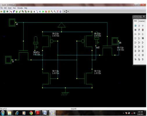
There is one another transistor is connected between the two cross coupled inverters that will help in reducing the effective resistance of the pull down network of inverters and is responsible for read operation by connected the gate of this transistor to the RWL (read word line) signal. Last one transistor also added in new proposed SRAM cell nearly one of the access transistor to create a separate path for read operation of new SRAM cell by connecting RWL signal with gate of this transistor and drain terminal is connected at output of one inverter. The schematic circuit of proposed SRAM is shown in figure (1.3)
Figure 1.3. Schematic circuit of proposed SRAM [6]
ISSN(Online): 2320-9801
ISSN (Print): 2320-9798
I
nternational
J
ournal of
I
nnovative
R
esearch in
C
omputer
and
C
ommunication
E
ngineering
(An ISO 3297: 2007 Certified Organization)
Vol. 3, Issue 6, June 2015
VI. SIMULATION RESULT DISCUSSION OF PROPOSED SRAM WITH CONVENTIONAL SRAM
WITH 0.6µm CMOS TECHNOLOGY
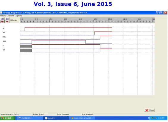
Here in this section by using microwind 2 layout designs and simulation, the proposed 10 T SRAM circuit analysis is done in term of calculating the total average power consumption during write operation as shown in figure (1.4.)& figure (1.5). This total average write power consumptions of proposed SRAM cell is compared with conventional 6T SRAM cell as shown in figure (1.7) and (1.8) for showing the actual reduction in power consumption in proposed SRAM cell.
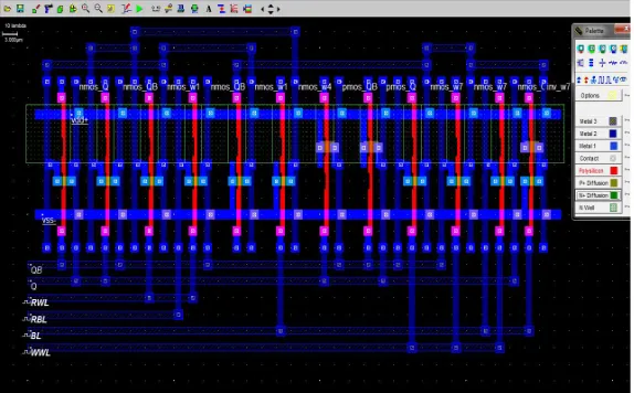
Figure 1.4 Layout design of proposed SRAM cell
ISSN(Online): 2320-9801
ISSN (Print): 2320-9798
I
nternational
J
ournal of
I
nnovative
R
esearch in
C
omputer
and
C
ommunication
E
ngineering
(An ISO 3297: 2007 Certified Organization)
Vol. 3, Issue 6, June 2015
Figure 1.6. Simulation waveform of proposed SRAM cell
From the simulation waveform result shown in figure (1.6), it is clear that during write operation WWL is high and RWL is low. Output Q goes high and QB low the write ‘1’ at Q & ‘0’ at QB is performed. As the WWL goes low and RWL goes high the output changes QB goes high and Q goes low, read ‘1’ operation is performed. The simulation result analysis of proposed SRAM shown in figure (1.5) shows the total average total average power consumption of proposed circuit during write operation.
ISSN(Online): 2320-9801
ISSN (Print): 2320-9798
I
nternational
J
ournal of
I
nnovative
R
esearch in
C
omputer
and
C
ommunication
E
ngineering
(An ISO 3297: 2007 Certified Organization)
Vol. 3, Issue 6, June 2015
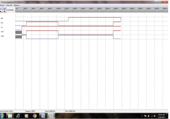
Figure 1.8. Simulation for conventional 6 T SRAM cell(P= 3.090mW)
Figure 1.9 Simulation analysis of 6 T SRAM cell
POWER CONSUMPTIONS
ISSN(Online): 2320-9801
ISSN (Print): 2320-9798
I
nternational
J
ournal of
I
nnovative
R
esearch in
C
omputer
and
C
ommunication
E
ngineering
(An ISO 3297: 2007 Certified Organization)
Vol. 3, Issue 6, June 2015
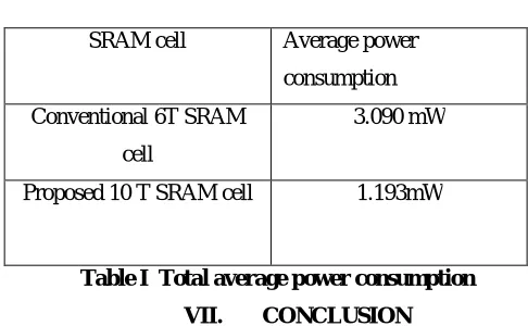
SRAM cell Average power
consumption
Conventional 6T SRAM
cell
3.090 mW
Proposed 10 T SRAM cell 1.193mW
Table I Total average power consumption
VII. CONCLUSION
In this paper by using of CMOS technology to 0.6µm technology a novel 10 T SRAM cell is designed. The proposed technique with two separate word line approach for read and write operation. The proposed SRAM used two tail transistors that are connected in pull down network of inverters, and these two tail transistors are cross coupled with bit line and bit bar line are responsible to reduce the number of times to charge and discharge the large bit lines capacitance to reduce the write power consumption. The simulation result using MICROWIND 2 TOOL shows much better decrease in write power consumption by using proposed SRAM cell as compared with conventional SRAM.
FUTURE WORK
With respect to day by day rapid advancement in CMOS technology, the proposed SRAM cell can be optimized to nano scale technology to decrease total power consumption during read and write operation as well as to control leakage current in standby mode
REFERENCES
[1] Abhishek kumar, “ SRAM Cell Design with minimum number of transistor” Proceeding of 2014 RAECS UIET Pnjab University Chandigarh 06-08 March, 2014
[2] International Technology Roadmap for Semiconductors by Semiconductor Industry Association, 2007.
[3] Kaushik Roy, Sharat Prasad, “Low-Power CMOS VLSI Circuit Design” Wiley, 2000 Integrated Circuit Engineering Corporation “Sram Technology” pp. 8.10- 8.
[4] Labonnah Farzana Rahman, Mohammad F. B. Amir, Mamun Bin Ibne Reaz,Mohd. Marufuzzaman, Hafizah Husain, “Advances on Low Power Designs for SRAM Cell” TELKOMNIKA Indonesian Journal of Electrical Engineering Vol. 12, No. 8, August 2014, pp. 6063 ~ 6082
[5] Singh AK, Prabhu CMR, Pin SW, Hou TC. A Proposed Symmetric and Balanced 11-T SRAM Cell for lower power consumption. TENCON. 2009: 1-4.
[6] Vertika Sarkari, Ajita Pathak, “ Design of low power MOS SRAM cell using 10 Transistor”, IJVES; Vol 06, Article 04564; May 2015; ISSN 2249-6556
[7] Kang &Leblebigi “CMOS Digital IC Circuit Analysis & Design”- McGraw Hill, 2003
[8] S. Mohan Das, K. S. Kiran Kumar, A.Madhulatha, “A Novel Low Power Energy Efficient SRAM Cell With Reduced Power Consumption using MTCMOS Technique” IOSR Journal of VLSI and Signal Processing (IOSR-JVSP)
Volume 5, Issue 1, Ver. I (Jan - Feb. 2015), PP 42-49 e-ISSN: 2319 – 4200, p-ISSN No. : 2319 – 4197
[9] Upadhaya P, Mehra MR, Thakur N “Low Power Design of an SRAM cell for portable devices” International conference or computer & Communication Technology (ICCCT’10) 2009: 255-259
[10] Abhishek Agal, Pardeep, Bal Krishan. 6T SRAM cell: Design and Analysis. IJERA; Volume 4, Issue 3(Version 1); March 2014; pp 574-577. [11] Sapna singh, Neha Arora, Meenkshi Suthar, Neha Gupta. Performance evaluation of different SRAM cell structures at different technologies. International Journal of VLSI design& communication systems (VLSICS); vol.3, No.1; February 2012.
[12]Uppunuthula Pavani Srinivas Kuntamalla “ A Low Power CMOS voltage mode SRAM cell for high speed VLSI Design” International Journal of Advances in Applied Science and Engineering (IJAEAS) ISSN (P): 2348-1811; ISSN (E): 2348-182X Vol-1, Iss.-4, SEPTEMBER 2014, 87-90 © IIST
[13] Microwind and Dsch v3.0 – Lite User’s Manual –Etienne Sicard.
[14] N. Yoshinobu, H. Masahi, K. Takayuki, K. Itoh. Review and future prospects of low-voltage RAM circuits. IBM journal of research and development; vol. 47, No. 5/6; pp.525-552; 2003
[15] L.Chang, et al. “Stable SRAM Cell Design for the 32 nm Node and Beyond”, VLSI Technology, 2005. Digest of Technical Papers. 2005 Symposium on, 14-16 June 2005 Page(s):128 -129
ISSN(Online): 2320-9801
ISSN (Print): 2320-9798
I
nternational
J
ournal of
I
nnovative
R
esearch in
C
omputer
and
C
ommunication
E
ngineering
(An ISO 3297: 2007 Certified Organization)
Vol. 3, Issue 6, June 2015
BIOGRAPHY
Vertika Sarkari is a student of M.Tech ECE in Department of Electrical Electronics Engineering, Amity School of Engineering & Technology Amity University Uttar Pradesh. Author research interests are low power VLSI Design, microelectronics and digital logic design.
Aditya Vikram Singh is a student of M.Tech ECE inDepartment of Electrical Electronics Engineering, Amity School
of Engineering & Technology Amity University Uttar Pradesh. Author research interests are Antenna Design and low power VLSI Design.
![Figure 1.3. Schematic circuit of proposed SRAM [6]](https://thumb-us.123doks.com/thumbv2/123dok_us/1483707.1181522/4.595.173.426.252.534/figure-schematic-circuit-proposed-sram.webp)