PN Sequence Preestimator Scheme for DS-SS Signal
Acquisition Using Block Sequence Estimation
Kwangmin Hyun
Division of Engineering, Wonju National College, Wonju-Si, Gangwon-Do 220-711, Korea
Email:[email protected]
Dongweon Yoon
Division of Electrical and Computer Engineering, Hanyang University, Seoul 133-791, Korea
Email:[email protected]
Sang Kyu Park
Division of Electrical and Computer Engineering, Hanyang University, Seoul 133-791, Korea
Email:[email protected]
Received 10 February 2004; Revised 12 June 2004; Recommended for Publication by Xiang-Gen Xia
Anm-sequence (PN sequence) preestimator scheme for direct-sequence spread spectrum (DS-SS) signal acquisition by using block sequence estimation (BSE) is proposed and analyzed. The proposed scheme consists of an estimator and a verifier which work according to the PN sequence chip clock, and provides not only the enhanced chip estimates with a threshold decision logic and one-chip error correction among the firstmreceived chips, but also the reliability check of the estimates with additional decision logic. The probabilities of the estimator and verifier operations are calculated. With these results, the detection, the false alarm, and the missing probabilities of the proposed scheme are derived. In addition, using a signal flow graph, the average acquisition time is calculated. The proposed scheme can be used as a preestimator and easily implemented by changing the internal signal path of a generally used digital matched filter (DMF) correlator or any other correlator that has a lot of sampling data memories for sampled PN sequence. The numerical results show rapid acquisition performance in a relatively good CNR.
Keywords and phrases:sequential estimation, PN sequence, acquisition, spread spectrum, digital matched filter.
1. INTRODUCTION
PN sequence acquisition is a precondition for stable and re-liable spread spectrum communication. The research on PN sequence acquisition has been continuing for more than 20 years to improve its performance, stability, and acquisition speed [1,2].
There are two representative methods for the acquisition of a PN sequence. One is a sequential estimation method that uses one of the important characteristics of the PN se-quence generation with linear feedback shift register (LFSR) structure. That is, ifmchips of the PN sequence can be es-timated correctly from the received signal, these chips can be loaded into them-shift-register generator to synchronize the system. In 1977, Ward and Yiu enhanced this method with recursive-aided sequential estimation [3]. In spite of its simple structure and rapid acquisition performance, this method cannot be used for low SNR radio environment because of the performance degradation and its instability. Several studies [4, 5, 6] have been done with a
majority-logic decoder to enhance the acquisition performance us-ing a large number of parity-check sums for each chip. Re-cently, a seed-accumulating sequential estimation scheme [7] has been proposed by accumulating each chip of the received seeds ofmchips, and another modified scheme [8] has been developed with a two-threshold decision logic which pro-vides not only chip estimates but also the reliability of the chip estimates by findingmconsecutive estimates.
m m−1 m−2 3 2 1
gm gm−2 gm−1 · · · g1 g0
+ + + +
Figure1: LFSR circuit for a generalizedm-sequence generator.
r(t) Long-term (kT
c) correlation and acquisition test with estimated PN sequence phase Local PN generator Estimated current-state register
State load
Tc
0 r(t)dt
Initial PN phase estimator
PN phase verifier PN sequence phase preestimator Figure2: Acquisition model.
Tc
0 r(t)dt
mchips
mchips
mchips Path control
Setupm+ 1 local PN generators Test with thresholdγ1
& select the possible path Verify with thresholdγ2
Estimating & verifying
control
Figure3: Detailed block diagram of the PN sequence phase preestimator.
(integration) period determine the structural complexity and acquisition performance of a digital matched filter (DMF) correlator.
Alternatively, we can adopt the adaptive detection scheme based on the MMSE (minimum mean-squared er-ror) criterion to successfully deal with the multiple-access interference or multiuser detection, which requires an esti-mation process, training with known data sequence, or blind channel estimation [11,12].
In this paper, we propose a preestimator scheme that can cooperate with a DMF correlator for PN sequence ac-quisition sharing the unused elements of the DMF structure within a given period of time (filling up the time of the DMF registers with the sampled PN chips or the given fixed op-eration time limits), and can analyze its performance. This scheme provides one-chip error correction capability of the initially loaded PN sequence chips on the LFSRs and a flexi-bility to manage structural resources of a correlator structure. In Sections2and3, the block sequence estimation (BSE) structure and its probabilistic performance are explained in detail, and the average acquisition time will be calculated inSection 4.Section 5gives numerical results that show the
acquisition performance of the proposed scheme. Finally, we conclude our work inSection 6.
2. PN SEQUENCE BLOCK ESTIMATOR
PN sequence generator corresponding to a generator polyno-mial has an LFSR form illustrated inFigure 1. In this figure, the boxes represent the shift register wheremis the number of the registers, circles containing subscripted letter coeffi -cientsgmrepresent a connection if the coefficient is a 1 or no
connection if the coefficient is a 0, and circles containing “+” mean modulo-2 adders or exclusive-OR gates [2]. The num-ber of shift registers, connection coefficients, and modulo-2 adders depends on a given generator polynomial. This gen-erator circuit is used for the local PN sequence gengen-erators of the proposed preestimator scheme. Because the explanation about this LFSR topic is beyond the scope of this paper, we will skip the details.
Figures2and3show a conceptual application diagram of the proposed scheme. This scheme consists of several compo-nents such as an integrator for chip durationTc, a bit slicer,
m 2 1 · · · 2m m+ 2 m+ 1
m Hamming distanc
e
m Hamming distanc
e
m Hamming distanc
e
Figure4: PN phase estimator.
PN sequence phase is estimated, this sequence can be loaded on a local PN generator and tested for a long time (given a period of timekTc), wherekis a positive integer. InFigure 2,
after finishing its operation with fail or success to estimate the correct PN sequence phase in a given operation time, the structure of the preestimator block will be disassembled and returned to the elements of the original correlator structure. The proposed PN sequence phase preestimator works as follows.
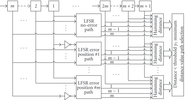
(1) Setupm+1 local PN sequence generators (LFSR paths) with the first receivedmPN chips as follows:
(1) loadmPN chips as the initial shift register values at a no-error LFSR path;
(2) loadmPN chips as the initial shift register values inverting position #1 chip at the error position #1 LFSR path;
(3) loadmPN chips as the initial shift register values inverting position #2 chip at the error position #2 LFSR path;
.. .
(m+ 1) loadmPN chips as the initial shift register values inverting position #mchip at the error position #mLFSR path.
(2) Receive the secondmPN chips and shift all LFSRs by
mtimes with a chip clock.
(3) Test the Hamming distance between the secondmPN chips and each register’s residue values of the LFSRs. (4) Select an LFSR path having minimum distance. (5) If the selected path’s minimum distance value is lower
than thresholdγ1, go to (6).
Else, go to (1) and repeat the previous steps because the estimating procedure failed.
(6) Receive the thirdm PN chips and shift the selected LFSR path bymtimes with the chip clock.
(7) Test the Hamming distance between the thirdmPN chips and the register’s residue values of the survived LFSR path.
(8) If the minimum distance is lower than thresholdγ2,
go to (9).
Else, go to (1) and repeat the previous steps because the verifying procedure failed.
(9) Optional test: long-termkTccorrelation and
acquisi-tion test with estimated PN sequence phase.
The above operation can be separated into two operators’ work. One is the estimator (works from step (1) to step (5)) inFigure 4that consists ofm+ 1 LFSR paths with one-error correction capability and chooses the best possible correct path. The other is the verifier (works from step (6) to step (8)) that confirms the survived path whether the selection is correct or not, as shown inFigure 5. The two operators’ comparator circuit has a very simple structure with an LFSR. For providing one-error correction capability to the estima-tor,m+ 1 local PN generator paths are needed as shown in
Figure 4.
After receiving the firstmPN chips, the no-error LFSR path stores these received mchips as themregister’s initial values, and othermlocal LFSR path register values are trans-ferred from the received buffers with one inverted chip that is corresponding to the chip error position buffer value to the path order of the local LFSR paths referred to inFigure 4. Among the m+ 1 local LFSR paths, the one path that sur-vived through the estimator test is assumed as a possible correct one. This test uses the Hamming distance compari-son method betweenm-time-shifted local LFSR paths’ regis-ter residue values and the second receivedmPN chip buffer values, path by path. After calculating the distances, we se-lect one path that has the minimum distance value among the LFSR paths, and the selected path’s Hamming distance is smaller than the given selection threshold γ1 to confirm
whether the choice is correct or not. Hence, we can assume that the selected LFSR path is a possible correct path by the estimator.
The selected local LFSR path shifted by anothermtimes with the chip clock will be compared with the third received
mPN chips and tested with the verification thresholdγ2at
Input
Figure5: PN phase verifier for the verification mode.
Table1: Number of registers.
Scheme Number of registers
BSE 240
DMF correlator (128 chip) 2 samples/chip 2048
4 samples/chip 4096
DMF correlator (256 chip) 2 samples/chip 4096
4 samples/chip 8192
To make all LFSR paths uncorrelated with each other due to the relationship between each LFSR path’s retained register values, the local LFSR path will be shifted more thanmtimes with the chip clock. Therefore, the proposed scheme can fin-ish all the estimation process in a minimum 3mPN chip time at the best case, and it is the basis of rapid acquisition.
In the case where the proposed BSE scheme is used with the DMF correlator, Table 1shows how many registers (bit memories) are required to implement the proposed scheme compared to a DMF correlator and gives an idea to share the furnished registers of a DMF correlator. We assume that the bits per PN chip sample are 8 and the length of the LFSR registermis 15.
3. DETECTION AND FALSE ALARM PROBABILITY
The probabilities of passing through the acquisition pro-cesses shown inFigure 6are defined inTable 2. These proba-bilities can be calculated with combinational probability.
To calculate each probability inTable 2, we assume that the received chip error probability is Pe at the given CNR.
The respective correct probability of the received PN chips to the incorrect path register values is 1/2, and to the correct path registers value is 1−Pe. That is, when one correct LFSR
path exists because there is none or one-chip error among the receivedmPN chips, the probability of the correct path selection will be calculate withPe, whereas if a correct LFSR
path does not exist or an incorrect LFSR path is selected, the following steps will use 1/2 instead ofPebecause the values in
them-time shifted LFSR and the newly receivedmPN chips can be assumed as uncorrelated random sequences for each other.
As shown inFigure 2, the received PN chips have a hard-decision value “1” or “0” by the bit slicer. Hence, all proba-bilities can be calculated based on Bernoulli trial cases.
In the process of selecting one LFSR path among one cor-rect and othermincorrect LFSR paths at the estimator, we can be faced up with selecting one of themincorrect LFSRs. This is due to the fact that the receivedmPN chips having multiple errors and there is no prior information about the correct path. There are two cases for the force to choose an incorrect path with the probabilityPPathMiss, in spite of one of
the local LFSR paths being the correct path. First is when one of the incorrect paths always wins over the correct path in the comparison test to reach the second receivedmPN chips with the probability PAF written as in (2). Multiple errors
(more than the thresholdγ1) in the receivedmPN chips to
test the Hamming distance can lead the test to this result. Sec-ond is when more than one of the incorrect paths’ Hamming distance testing results is equal to the correct path’s. In this case, one of these paths will be selected arbitrarily and this choice can be incorrect with the probabilityPEFexpressed as
in (3). Therefore,
If a successful acquisition of the PN sequence with the detection probabilityPDin (5) is declared, the receiver starts
Estimation mode Verification mode
1stmchips 2ndmchips 3rdmchips Correct
acquisition alarmFalse
Acquisition miss Figure6: Acquisition process diagram.
Table2: Probability definitions.
Probability Definition
PC Probability of the one correct path existence amongm+ 1 LFSR paths
PDet Probability of the correct path selection amongm+ 1 LFSR paths
PNDet Probability of the one path selection among all incorrect LFSR paths
PPathMiss Probability of missing the correct path at the estimator
PAcq Probability of the acquisition declaration at the verifier
PFA 1 Probability of the false acquisition declaration withPPathMissat the verifier
PFA 2 Probability of the false acquisition declaration withPNDetat the verifier
PN generator for a more reliable acquisition process:
PD=PCPDetPAcq, (5)
However, even though the acquisition is declared, if the procedure is passed through the “verify incorrect case” node in Figure 6, it results in a false alarm with probabilityPFA
given by
Contrary to the false alarm case, there are two missing cor-rect LFSR path cases. First isPPathMissfrom the estimator, and
second is 1−PAcqfrom the verifier. Hence, we can calculate
the missing probability as follows:
PMiss=PCPPathMiss+PCPDet
1−PAcq
. (9)
4. AVERAGE ACQUISITION TIME
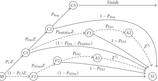
The signal flow graph of the PN code acquisition scheme is shown inFigure 7. After the acquisition declaration, nor-mally to verify whether the acquisition declaration is correct or not, a long-time verification device, such as a matched filter correlator, should be adopted. To analyze the perfor-mance of the proposed acquisition scheme, if the scheme is declared as a correct acquisition, then the verification device will detect the PN sequence successfully.
The transfer function can be calculated with time delayZ
as follows:
F(Z)=PCPDetPAcqZ2
1−R(Z) , (10)
whereRR(Z) represents the sum of signal flow transfer
func-tions that have time delay because of the acquisition fail, and is computed from
PCZ
Figure7: Signal flow graph.
In (11),RF1(Z),RC1(Z), andRC2(Z) are defined, respectively,
TheTeis the penalty time to be wasted at the additional
verification device, such as a matched filter correlator, be-cause of the false alarm.
With this transfer function, the average acquisition time can be calculated by differentiating the transfer function and letting the time delay componentZ=1, resulting in
TAcq= d
where Ta is the m-chips receiving time, the examination
time, filling up the registers of the LFSR with sampled chips and withm-time LFSRs shifted with the chip clock.
5. NUMERICAL RESULTS
In this paper, this chip error probability will be considered under an additive white Gaussian noise (AWGN) channel where its two-sided power spectral density is N0/2. Also
BPSK modulated signal with thePein (14) is assumed:
Pe=Q
whereECis the one-chip energy.
For the numerical calculations derived in the previous sections, the register lengthmof the LFSR PN sequence gen-erator is 15. The penalty time Te for the false alarm is
as-sumed as 128Tc.
In Figures8and9, the detection and false alarm prob-abilities are plotted versus CNR with given γ1,γ2.Figure 8
shows that the detection probability plots continuously rise improving the acquisition performance until the saturation near 0 dB. In Figure 9, the false alarm probability nearly comes to be saturated at low CNR (worse than−5 dB) be-cause there can be multiple error chips among the received
m PN chips to be loaded into the estimator’s initial value, the acquisition and false alarm probabilities are small. In mid CNR (nearly from−5 dB to−5 dB), even though the estima-tor estimates the correct PN sequence phase, the false alarm probability can increase due to the erroneous received PN chips used for the Hamming distance test and the decision operation at the estimator and the verifier.
Figures10and11show the average acquisition time per-formances as a function of the givenγ1 andγ2parameters.
Clearly, it is shown that the proposed structure can achieve rapid acquisition performance, especially when CNR is bet-ter than−5 dB.
Figure 12shows the comparison of the average acquisi-tion time performance of the proposed BSE scheme in the case ofγ1 =γ2 =3 with several other acquisition schemes:
the recursion-aided sequential estimation (RASE) scheme [3] and the synchronization schemes using matched filter and fixed integration methods [2]. To calculate the average acquisition time of the matched filter and the fixed integra-tion methods, we assume the best-probability case (lower-bound), PD = 1 andPFA = 0. In addition, to be fair to
the referenced schemes, the penalty time and the integration time are set the same as 128Tc. FromFigure 12, we can find
100
10−1
10−2
10−3
10−4
10−5
Det
ection
p
ro
babilit
y
(
PD
)
−10 −5 0 5
Eb/N0(dB)
r1=1,r2=3
r1=2,r2=3
r1=3,r2=3
r1=4,r2=3
Figure8: Detection probabilityPDversus CNR, with givenγ2=3
andγ1.
10−3
10−4
10−5
F
alse
alar
m
pr
obabilit
y
(
PFA
)
−15 −10 −5 0 5 10
Eb/N0(dB)
r1=1,r2=3
r1=2,r2=3
r1=3,r2=3
r1=4,r2=3
Figure9: False alarm probabilityPFAversus CNR, with givenγ2=3
andγ1.
6. CONCLUSIONS
In this paper, a PN sequence preestimator scheme using the BSE was proposed for the direct-sequence spread spectrum (DS-SS) system. The estimator, a part of the proposed BSE scheme, provides the enhanced chip estimates with threshold decision logic and one-chip error correction among the first mreceived chips. The one-error correction capability of the estimator is entitled by them+ 1 local PN sequence generators. The verifier is used for the reliability check of the estimates with additional decision logic. From the numerical analysis, we observed that the average acquisition time is faster than the other referenced schemes in this paper. In special, the BSE scheme kept up fast acquisition time
106
105
104
103
102
A
ve
rag
e
ac
q
uisitio
n
time
TAc
q
(c
hips)
−15 −10 −5 0
Eb/N0(dB)
r1=1,r2=3
r1=2,r2=3
r1=3,r2=3
r1=4,r2=3
Figure10: Average acquisition timeTAcqversus CNR, with given
fixedγ2=3 andγ1.
106
105
104
103
102
A
ve
rag
e
ac
q
uisitio
n
time
TAc
q
(c
hips)
−15 −10 −5 0
Eb/N0(dB)
r1=3,r2=1
r1=3,r2=2
r1=3,r2=3
r1=3,r2=4
Figure11: Average acquisition timeTAcqversus CNR, with given
fixedγ1=3 andγ2.
until the CNR is fallen near to −4 dB. The high hardware complexity of the proposed BSE scheme is affordable when the DMF correlator has already been used. That is, because the component parts of the proposed scheme are similar to those of the DMF correlator or any other correlator which has many memory elements, it can be easily implemented by changing the signal path connections and adding minimized glue logics.
1010
Figure12: Comparison of average acquisition time with the pro-posed BSE, RASE, matched filter correlator, and fixed integration time case.
REFERENCES
[1] M. K. Simon, J. K. Omura, R. A. Scholtz, and B. K. Levitt,
Spread Spectrum Communication. Vol. III, Computer Science
Press, Rockville, Md, USA, 1985.
[2] R. L. Peterson, R. E. Ziemer, and D. E. Borth, Introduction to
Spread Spectrum Communications, Prentice Hall, Englewood
Cliffs, NJ, USA, 1995.
[3] R. B. Ward and K. P. Yiu, “Acquisition of pseudonoise signals by recursion-aided sequential estimation,” IEEE Trans. Com-mun., vol. 25, no. 8, pp. 784–794, 1977.
[4] C. C. Kilgus, “Pseudonoise code acquisition using majority logic decoding,”IEEE Trans. Commun., vol. 21, no. 6, pp. 772– 774, 1973.
[5] G. L. Stuber, J. W. Mark, and I. F. Blake, “Sequence acquisition using bit estimation techniques,”Information Sciences, vol. 32, no. 3, pp. 217–229, 1984.
[6] R. T. Barghouthi and G. L. Stuber, “Rapid sequence acqui-sition for DS/CDMA systems employing Kasami sequences,”
IEEE Trans. Commun., vol. 42, no. 2/3/4, pp. 1957–1968, 1994.
[7] J. H. Lee, I. Song, S. R. Park, and J. Lee, “Rapid acquisition of PN sequences with a new decision logic,”IEEE Trans. Veh.
Technol., vol. 53, no. 1, pp. 49–60, 2004.
[8] S. Yoon, I. Song, and S. Y. Kim, “Seed accumulating sequential estimation for PN sequence acquisition at low signal-to-noise ratio,”Signal Processing, vol. 82, no. 11, pp. 1795–1799, 2002. [9] A. Polydoros and C. L. Weber, “A unified approach to serial search spread-spectrum code acquisition—Part I: general the-ory,”IEEE Trans. Commun., vol. 32, no. 5, pp. 542–549, 1984. [10] A. Polydoros and C. L. Weber, “A unified approach to serial search spread-spectrum code acquisition—Part II: a matched-filter receiver,” IEEE Trans. Commun., vol. 32, no. 5, pp. 550–560, 1984.
[11] S. G. Glisic, Adaptive WCDMA: Theory and Practice, John Wiley & Sons, New York, NY, USA, 2003.
[12] J. H. Cho and J. S. Lehnert, “Blind adaptive multiuser detec-tion for DS/SSMA communicadetec-tions with generalized random spreading,” IEEE Trans. Commun., vol. 49, no. 6, pp. 1082– 1091, 2001.
Kwangmin Hyun received the B.S., M.S., and Ph.D. degrees in electronic communi-cations engineering from Hanyang Univer-sity, Seoul, Korea, in 1989, 1995, and 2004, respectively. In 1989, he joined Radio Com-munications System Laboratory, Daewoo Telecom Inc., Korea. From 1995 to 1996, he worked at the Institute of Advanced Engi-neering (IAE) and from 1997 to 2001, at KMW Inc., Korea. From March 2002 to
Au-gust 2004, he was an Adjunct Professor in the Division of Telecom-munication, Dong-Ah Broadcasting College, Ansung, Korea. Since March 2005, he has been with the Division of Engineering, Wonju National College, Wonju-Si, Gangwon-Do, Korea. His research in-terests are in the areas of communications theory, wireless commu-nications, mobile commucommu-nications, multicarrier commucommu-nications, UWB communications, and signal processing for digital wireless systems.
Dongweon Yoonreceived the B.S. (summa cum laude), M.S., and Ph.D. degrees in elec-tronic communications engineering from Hanyang University, Seoul, Korea, in 1989, 1992, and 1995. From March 1995 to Au-gust 1997, he was an Assistant Professor in the Division of Electronic and Informa-tion Engineering, Dongseo University, Pu-san, Korea. From September 1997 to Febru-ary 2004, he was an Associate Professor in
the Division of Information and Communications Engineering, Daejeon University, Daejeon, Korea. Since March 2004, he has been on the faculty of Hanyang University, Seoul, Korea, where he is now an Associate Professor in the Division of Electrical and Computer Engineering. He has twice been an Invited Researcher at the Elec-tronics and Telecommunications Research Institute (ETRI), Dae-jeon, Korea, from February to December 1997, and from Novem-ber 2002 to March 2004. He was a Visiting Professor at the Penn-sylvania State University, University Park, PennPenn-sylvania, for the academic year 2001–2002. He has served as a Consultant for a number of companies and has given many lectures on the top-ics of digital communications and wireless communications. His research interests include new modulation techniques, accurate performance evaluations, digital communications theory and sys-tem, spread spectrum communications, and wireless communica-tions.
Sang Kyu Park received the B.S. degree from Seoul National University, Korea, in 1974, the M.S. degree from Duke Univer-sity, USA, in 1980, and the Ph.D. degree from the University of Michigan, USA, in 1987, all in electrical engineering. From July 1976 to October 1978, he was a Re-search Engineer at the Agency for Defense Development, Korea. From August 1990 to August 1991, he was a Visiting Scholar at