Delay Analysis for Current Mode Threshold Logic Gate Designs
DHANAVATH KIRAN KUMAR NAIK [email protected]
Abstract: Current mode is a popular CMOS-based implementation of threshold logic functions, where the gate delay depends on the sensor size. This paper presents a new implementation of current mode threshold functions for improved gate delay and switching energy. An analytical method is also proposed to identify optimum sensor sizes that minimize the gate delay. This allows us to design large threshold functions with delay much less than a network of CMOS gates. Simulation results on different gates implemented using the optimum sensor size indicates that the proposed current mode implementation method outperforms consistently the existing implementations in delay as well as switching energy.
Keywords: Current mode, operating speed, sensor sizing, threshold logic gates (TLGs).
I.INTRODUCTION
Threshold logic gates (TLG) are an attractive alternative for implementing digital circuits. Methodologies for implementation of circuits using TLG become available and thus the synthesis of efficient TLG based circuits becomes feasible. An existing issue is to optimize the performance of a TLG gate by selecting appropriate transistor sizes. An alternative to time consuming exhaustive SPICE simulations is presented and evaluated. It is based on an analytical method capable of providing near optimum sensor sizes for the circuit implementing the TLG. It is also capable of providing the expected gate delay without time consuming simulation steps; thus improving the performance of TLG based synthesis methodologies. It is expected that the exponential savings in performance of digital circuits due to parameter scaling will evaporate soon [4-8]. Alternative technologies, such as multiple valued logic, threshold logic gates, and others, can extend parallel processing capabilities [4-8].
Monostable–Bistable Transition Logic Element (MOBILE), neuron MOS, single electron technology are few examples of threshold logic gate implementations [6, 9, 10, 13]. A Threshold Logic
Gate (TLG) is a N-input device which calculates the weighted sum of inputs [3]. A basic TLG consists of N-inputs, a weight value for each input, and a threshold weight. The sum of the input weights is compared with the threshold weight. If it is greater than the threshold weight, then the digital output of TLG is logic high, and if it is less it will be logic zero [3]. In the CMOS-based implementation considered in this paper, when the sum of the input weights is equal to the threshold weight, then the gate is in undefined state. Weights are selected so that this case is avoided.
The equation representing output of a TLG is given as
where wi is the weight of the ith input, xi is the input
applied to the ith input, and wT is the threshold weight
for the function f of a TLG. The input weights can be either positive or negative but the threshold weight is always positive. In this paper, an N-input function with P positive weights is denoted as {w1, . . . , wP : wT ,
wP+1, . . . , wN }.
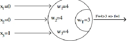
Example 1: Consider a function f = x1 + x2 + x3 with
weight configuration (w1, w2, w3 : wT ), where w1, w2,
and w3 correspond to the weights of the inputs x1, x2,
and x3, respectively, and wT is the threshold weight. A
possible weight configuration is {w1, w2, w3 : wT } =
{4, 4, 4 : 3}, where all the input weights are positive. When applying the input pattern {x1, x2, x3} = {0, 0,
1}, the weighted sum of inputs is 4 · 0 + 4 · 0 + 4 · 1 > 3, and, according to (1), f = 1. See also Fig. 1. Function f is denoted as {4, 4, 4: 3}.
This paper considers implementations of threshold logic functions using current mode. This is a popular CMOS-based approach. All current mode implementation methods considered in this paper consist of two parts: the differential part and the sensor part. The number of transistors in the sensor part is constant and does not depend on the implemented function. The number of transistors in the differential part depends on the sum of input weights and the threshold weight.
There exist two approaches for implementing current mode TLGs: the current mode TLG (CMTLG) [1] and the Differential current mode logic (DCML) [11]. Section II reviews these two approaches.
Section III presents a new implementation, which we call the dual clock current mode logic (DCCML), which results in both speed and switching energy [power-delay product (PDP)] improvements over the approaches in [1] and [11]. They consist of two parts: the differential part and the sensor part. All the pMOS transistors in the sensor part have the same size S, which we call the sensor size. The sensor size impacts the performance of all the three current mode implementations for any threshold logic function. It is a very time-consuming task to obtain the optimum sensor size through iterative SPICE simulations, one simulation for a different sensor size.
Section IV presents the second contribution of this paper, which is an analytical approach to determine quickly and accurately the appropriate sensor size S for a given function under any existing current mode approach, such as those in [1] and [11] and the proposed implementation in Section III. Section V presents simulation results that demonstrate the accuracy of the optimum sensor identification method in Section IV. It also presents results that show that the current mode approach in Section III consistently outperforms those in [1] and [11] on delay as well as switching energy. Finally, Section VI concludes.
II. CMTLG AND DCML IMPLEMENTATIONS OF A THRESHOLD LOGIC FUNCTION
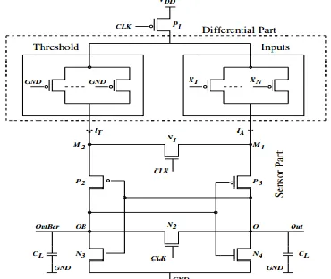
MTLG is a CMOS based implementation of TLG shown in Figure 2 [1]. The CMTLG can be divided into two parts, the differential part and the sensor part. The differential part can be subdivided into
threshold part and the input part all the transistors are connected in parallel. The transistors in the threshold part are always ON and the total current flowing through the threshold part is represented as Threshold current IT. The number of PMOS active (ON) in the
input part depends on the input pattern applied. The total current passing through the input side for a particular input pattern is represented as the Active Current IA. The nodes connecting the differential part
and the sensor part on the input side and the threshold side are M1 and M2, respectively and nodes O and OB
are the output nodes and are shown in Figure 2.
The nodes connecting the differential part and the sensor part on the input side and the threshold side are M1 and M2, Fig. 3. Output voltages and their difference in the two clock phases for CMTLG. respectively. The sensor part has three pMOS transistors P1, P2, P3, and four nMOS transistors N1, N2, N3, and N4 as shown in Fig. 2. If the size of the sensor is S, then all the pMOS transistors in the sensor part have S μm size and all the nMOS transistors in the sensor part have a size smaller than S μm.
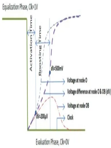
The operation of the CMTLG is divided into two phases [1]: the equalization phase and the evaluation phase. These phases are explained with the help of Figs. 2 and 3. When the applied clock (clk) to the CMTLG is high, then the circuit is in the equalization phase. When clk is low, then the circuit is in the evaluation phase [1]. In the equalization phase, transistors N1 and N2 are ON, nodes M1 and M2 have the same voltage because of transistor N1, and nodes O and O B have the same voltage because of transistor N2 (see also Fig. 2). In the evaluation phase, transistors N1 and N2 are OFF, and if the threshold current is less than the active current, then the voltage at node O rises faster than that at node O B [1]. If during the evaluation phase the threshold current exceeds the active current, then the voltage at node O B rises faster than that at node O [1].
Figure 2: Current Mode Threshold Logic Gate
Figure 3 shows the two phases of the clock, the voltage at output nodes O and OB and the voltage difference between nodes O and OB (dV). The delay of a CMTLG can be divided into two phases, the activation time and the boosting time. The first phase is the time taken by CMTLG to develop a small voltage difference (200μV) across the output nodes O and OB [1]. In this phase, the difference between IA and IT
leads to gradually increasing voltage difference between the nodes M1 and M2 also increases. The time
taken by the CMTLG to develop initial voltage difference is represented as the activation time TA. The
second phase is the time taken by the sensor (the back to back connected inverters) to boost the initial voltage difference to a logic state at the output nodes. This time is referred as the boosting time (TB).
The activation time depends mainly on the differential part. The second phase is the time taken by the sensor part (the back-to-back connected inverters) to boost the initial voltage difference to a logic state at the output nodes. This time is referred to as the boosting time TB. The boosting time depends mainly on the sensor part.
Figure 3: Behavior of output voltages and their voltage difference in two phases of clock
An alternative differential clock threshold logic implementation is presented in [11], and it is referred to as the differential current mode logic (DCML) approach. Its block diagram is shown in Fig. 4. It is also divided into the differential part and the sensor part. The currents through the threshold part and the inputs part are also denoted by IT and IA, respectively. The sensor part consists of four pMOS transistors, labeled P1–P4, and six nMOS transistors, labeled N1–N6. The load capacitance CL is applied to both the output nodes O and OB.
Fig. 4: Block diagram of differential current mode logic.
than IA, then the voltage at OB rises faster than the voltage at O and low voltage results at OB.
Fig. 5: Output voltages and their difference in the two clock phases for DCML.
Fig. 5 shows the two phases of the clock, the voltage at nodes O and OB, and the voltage difference between O and O B (dV). The delay of DCML is divided into the activation time TA and the boosting
time TB.
A method to obtain optimum sensor sizes:
The CMTLG of [1] assumes that all inputs have minimum weights. If a TLG requires weight wi >
1 (greater than minimum weight) for some input i, then as an alternative we can implement the function with wi
minimum weight inputs for CMTLG of Figure 2.
We consider an N-input CMTLG of [1] that can be used to implement different TLG functions for a given value of N and T. This section shows how to identify optimum sensor size for the N-input CMTLG of [1], so that the delay of any TLG implemented by the N-input CMTLG is minimized.
III. LOW POWER AND HIGH-SPEED DUAL-CLOCK-BASED CURRENT MODE TL
IMPLEMENTATION
A new TLG implementation is proposed. It is called DCCML. As the name indicates, two clocks are used to achieve low power consumption and high speed.
The approach consists of two steps. First, the set of functions that can be implemented using CMTLG for a given input configuration (number of inputs N and threshold T) are grouped in to equivalent classes. We show that when T+1 inputs are active on the input side then the TLG exhibits its worst delay.
The block diagram DCCML is shown in Fig. 6. As in previous approaches, the DCCML is divided into two basic blocks: the differential block and the sensor block. The differential block is further divided into four blocks: the positive threshold, the negative inputs, the negative threshold, and the positive inputs. All the transistors in the differential block are equal-sized pMOS transistors and are connected in parallel, as shown in Fig. 6. The sensor block consists of six pMOS transistorsP1···P6 and three nMOS transistors
N1, N2, and N3. The gates of transistors P1 and N1 are
connected to Clk1 and the gates of transistors P2, P5,
and P6 are connected to Clk2. Transistor N1 acts as an
equalizing transistor and it equalizes the voltage at nodes OP and OPB. Transistors P5 and P6 isolate the
differential block from the sensor block.
The transistors in the positive threshold and negative threshold are always active. Transistors in the positive and negative inputs blocks are active depending upon the input pattern applied. The input pattern applied for the positive inputs block is denoted by {x1, x2, . . . , xI . Let N denote the number of inputs,
Fig. 6: Block diagram of DCCML TLG
Consider a function f, with a possible weight configuration {w1, w2 : wT , w3, w4}={2, 2:3, −1, −1}.
In the given weight configuration, we have two positive weights w1 and w2 and two negative weights
w3 and w4. Weights w1 and w2 are implemented in the
positive inputs section and weights w3 and w4 are
implemented in the negative inputs section. The threshold weight wT is implemented in the positive
threshold section.
The current through the four blocks (positive threshold, negative inputs, negative threshold, and positive inputs) are denoted by IPT , INI , INT , and IPI ,
respectively. The currents through transistors P5 and P6
are denoted by IP5 and IP6 . Here, IP5 = IPT + INI and IP6 =
INT + IPI . Nodes OP and OPB are the output nodes. The
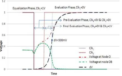
load capacitance is denoted by CL. The operation is divided into three phases: the equalization phase, the pre-evaluation phase, and the final-evaluation phase. When clocks Clk1 and Clk2 are high, then the circuit is in the equalization phase. When clocks Clk1 and Clk2 are low, then the circuit is in the pre-evaluation phase. When Clk1 is low and Clk2 is high, then the circuit is in the final-evaluation phase. See also Fig. 7.
It is noted that when the two clocks are not completely aligned the operation of the gate is not affected. The possible cases of misalignment are: 1) the falling edge of Clk2 comes before the falling edge of
Clk1 and 2) the falling edge of Clk2 comes after the falling edge of Clk1.
Fig. 7: Clocks in DCCML.
In the first case, the current from the differential part is equalized because of transistor N1 and the evaluation phase starts after the falling edge of Clk1. In the second case, there will be no current from the differential part as Clk2 is not active yet. Hence, the pre-evaluation phase starts after the falling edge of Clk2. The implementation avoids a very early arrival of Clk1. In that case, a nonstable signal might result in erroneous output.
If the current IP6 through the pMOS transistor
transistor P5, then the voltage at the output node OP rises faster than the output node OPB. As a result, high voltage is obtained at output node OP and low voltage occurs at output node OPB. Otherwise, the voltage at the output node OPB rises faster than the output node OP. As a result, high voltage is obtained at the output node O P B and low voltage is obtained at node OP.
In DCCML, the pMOS transistors P1, P2, P5,
P6 and the pMOS transistors in the differential block
are used to provide the initial voltage at the output nodes OP and OPB. Using Clk2, we restrict the current flow from the differential block to the sensor block, once initial voltage difference is established at the nodes OP and OPB; in this way we stop the current flowing from the differential block to the sensor block. Using Clk2, we are able to minimize power consumption in the circuit. Transistors P5 and P6 are
also used to isolate high capacitance circuit block (the differential block) at the output nodes. Hence, in the final evaluation phase the sensor block drives the load capacitance as well as the capacitance from a single transistor P5 or P6. Delay is reduced because the
duration of the final evaluation phase is small. The voltage at the output nodes OP and OPB and the voltage difference (dV) at the output nodes OP and OPB are shown in Fig. 8 for the three clock phases.
Fig. 8: Voltage at output nodes OP and OPB and dV during the three clock phases.
In particular, the delay of the DCCML is divided into two time phases: the activation time and the boosting time. The activation time is the time taken by the circuit to develop an initial voltage difference at the output nodes OP and OPB. The boosting time is the
time taken by the DCCML to bring the initial voltage to the correct voltage at the output nodes OP and OPB. In the pre-evaluation phase, both the differential part and the sensor part are active, and therefore the activation time is not affected. In the final evaluation phase, the differential part is kept inactive using Clk2. Therefore, the effect of internal capacitance due to the differential part is isolated. Hence, it takes very little time to boost the outputs to the final value. The power is also reduced due to the isolation of the differential part.
IV. DELAY MINIMIZATION BY AN APPROPRIATE SENSOR SIZE SELECTION
This section presents an analytical formula to compute the sensor size that minimizes the gate delay. Let N denote the number of inputs, N the sum of all positive input weights, and T the sum of the threshold weight and negative input weights Our analysis assumes that all the input weights are connected in parallel, and that each weight wi can be implemented by wi unit width pMOS transistors connected in parallel. This is an accurate assumption. We have implemented TLG weights using a smaller number of wider pMOS transistors connected in parallel and SPICE simulations showed no difference in the performance of the TLG. This is further explained in the example below.
Example 2: Consider a threshold function where N, the sum of positive input weights, is 11. Let also T , the sum of the threshold weight and negative input weights, be 4. In this function, we have (N, T) = (11, 4). Gates {11:4}, {6, 5: 4}, {5, 5, 1: 4}, {5, 4, 1, 1: 4}, {4, 4, 1, 1, 1: 4}, and {1, 1, 1, 1, 1, 1, 1, 1, 1, 1, 1: 4} were implemented in the 45-nm technology. SPICE simulation shows an identical delay of 297 ps.
The proposed method considers that the TLG operates under an input pattern that exhibits the worst case propagation delay, and then focuses on deriving an analytical model that expresses TLG delay in terms of the sensor size S in that setting. In a first step, we identify the pattern that gives the highest delay for the function. In a second step, we consider this worst case scenario, and the delay will be expressed as a function of the sensor size S. Then, we operate on that function in order to optimize the sensor size S.
In the first step, it is shown that when T +1 inputs are active then the TLG exhibits its worst delay. Let NA = ∑i wi , such that xi = 1. Such inputs i are
called active, and the respective pMOS transistors are also called active. Assume that the initial current flowing through an active minimum-sized pMOS is Ip.
Then the current flowing through the threshold side of the TLG is T · I p, and the current flowing through the
input side for NA inputs being active is NA · Ip. To
obtain the worst case delay for logic 1 at the output node O, the current difference IA− IT should be
minimum.
For logic 0, this current difference should also be minimum. Since transistors on the threshold side are always ON, the maximum delay for a rising transition of the output is obtained when we have T + 1 active transistors. Likewise, T − 1 active transistors tend to obtain the worst case delay for a falling transition at the output. However, it is known that the worst case delay occurs for rising output transition [1]. Hence, a worst case delay pattern is one that gives the least current difference at nodes M1 and M2. The following is an example where SPICE simulations confirm this analysis.
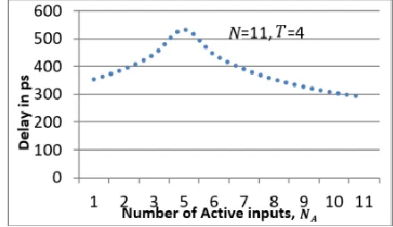
Example 3: Consider a CMTLG implementation of a function with T = 4, N = 11, and sensor size S = 10. The input pattern that has T + 1 number of active inputs gives the worst delay. Hence, the highest delay encountered is NA = 5. Fig. 9 shows the delay of the TLG using SPICE in 45-nm technology. When NA varies in range [5], [11], the output transition is rising, and the highest rising delay occurs when NA = 5. When NA is in the range (0, 5) the transition at the output is falling and in that case the delay is less.
Fig. 9: CMTLG delay with N = 11 and T = 4 as NA varies.
Similar behavior has been observed for different values of T and N. Furthermore, extensive SPICE simulations have confirmed that the worst case delay of DCML gates is obtained when NA = T + 1 and
also occurs when the output is rising.
In the second step of the proposed method, it is shown how to obtain an analytical expression that approximates the time delay TD as a function of the
sensor size S, given N and T . The delay time TD is
divided into two phases: the activation time TA and the
boosting time TB. The tradeoff among the two phases is
analyzed by varying the sensor size S and keeping all the other parameters N, T , and NA constant.
During the activation time, the major current component is the current from the differential part. From the schematics in Figs. 2 and 4, due to the voltage difference at nodes O and OB, we conclude that |IA − IT | is proportional to |NA − T|. The time
requirement for the activation time will be inversely proportional to the current. The time will be proportional to a charge that depends on two components: the voltage difference that is required at the end of the activation phase and the capacitance that the differential part is driving. This capacitance is the difference in the differential capacitance N · Ci’ − T ·
CT’ , where Ci’ and CT’ are the unit capacitances of the
input part and the threshold part, the sensor capacitance, which is S · C’s where C’s is unit
CL/|NA − T|). Term (N · Ci’ − T · CT’ + CL/|NA − T|) is
invariant to the sensor size and term (S · C’s /|NA − T|)
is proportional to S.
During the boosting time, the delay depends on the current provided by the sensor. This current will be proportional to the sensor size. The capacitance to be charged will be the same as in the activation time. (The voltage will be different, which does not depend on the sensor size S.) Hence, the boosting time will be proportional to (N · Ci’ − T · CT’ + S · C’s + CL/S). The
numerator is an approximation to the overall capacitance connected to the outputs O and OB. The boosting time consists of (S · C’s /S) = C’s , which is
invariable to the size of the sensor and (N · Ci ’
− T · CT’ + CL/S), which is inversely proportional to the
sensor size.
We conclude that the gate delay consists of three components T0, T1, and T2 defined below. Component T0 is invariant to S and that is the sum of the invariant components of the activation time and the invariable components of the boosting time, i.e., T0 = C’s + (N · Ci’ − T · CT’ + CL/|NA − T|). Component T1
is proportional to the sensor size S and occurs during the activation time, i.e., T1 = C’s · |(1/NA − T )|.
Finally, component T2, which is inversely proportional to the sensor size, occurs during the boosting time and is equal to N · Ci
’− T · C T
’
+ CL. Concluding, the overall time TD is estimated as
By applying regression analysis on SPICE simulations, TD is rewritten as
with ε0 ∈ (0, 5), ε1 ∈ (0, 20), and ε2 ∈ (0, 5). All the ranges are expressed in picoseconds. Here a, b, c, and d
are constants and their values are a = 1e − 9, b = 1 for CMTLG, DCML and b = 0.1 for DCCML, c = 1e − 11, and d = 3.86e − 2. Equation (3) gives the gate delay for different sensor sizes for fixed values of N, T , NA, and
CL.
The final step of the proposed method operates on (3) in order to derive sensor size Sopt, which gives the minimum gate delay. Sensor size Sopt is derived by applying the first derivative on (3) and equating it to zero in order to find the minimum value of TD. We have that
The remainder of this section presents the corollaries obtained by (3).
Corollary 1: The delay TD decreases with an increase
in S, reaches an optimum value for some consecutive values of S, and then increases as S increases. The actual values of minimum S depend on N and T.
Corollary 2: For a sensor size that is smaller than the optimum sensor size Sopt, the activation time TA is low
and the boosting time TB is high. The activation time is less because it has less capacitance and the output can drive this small capacitance faster to develop an initial voltage difference. In order to boost the initial voltage difference, the back-to-back connected inverters must be small. Hence, the boosting time is high.
Corollary 3: For a sensor size that is larger than the optimum sensor size Sopt, the activation time TA is high
and the boosting time TB is low. The activation time is
high because it may have a large capacitance and the output is slow to develop an initial voltage difference. Large back-to-back connected inverters will boost the initial voltage difference quickly.
Corollary 4: TD decreases as S approaches Sopt and
then increases as S grows larger than Sopt. The corollary is justified because the total delay TD of TLG
is the sum of TA and TB.
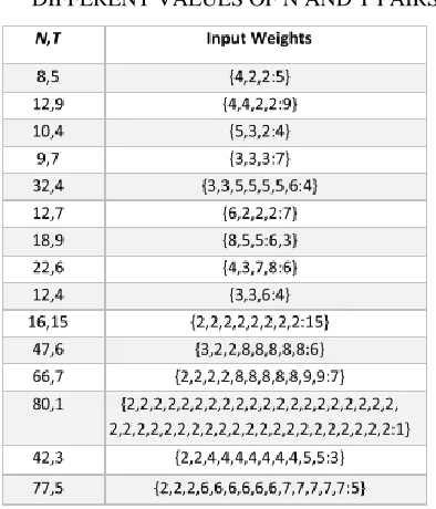
This area shows the reenactment comes about that exhibit the effect of the sensor measure enhancement strategy in Section IV and the DCCML approach in Section III. The assessment in this area was led on arbitrarily chose edge rationale capacities portrayed by the individual (N, T) values, where N means the whole of the positive info weights and T signifies the entirety of the limit weight and negative information weights. Table I records a portion of the capacities. The primary section in Table I gives the N and T esteems. The second segment in Table I records the positive information weights, trailed by ":", took after by the edge weight, and after that by the negative info weights. For instance, work (18, 9) in the seventh line has three positive info weights and a negative information weight.
TABLE I
FUNCTIONS THAT CORRESPOND TO DIFFERENT VALUES OF N AND T PAIRS
Every one of the capacities were executed in 45-nm CMOS innovation with DCCML and the methodologies in [1] and [11]. The clock voltages were set to 1 V for high voltage and 0 V for low voltage, and the heap capacitance CL was 30fF. The channel length was set to the base an incentive for all transistors. All the info pMOS transistors and limit pMOS transistors
had a240 − nm width measure, which is the base transistor width. Weights of significant worth higher than one were executed by associating the unit-sized pMOS transistors in parallel.
The initial segment of this segment exhibits the point by point reenactments that decide the effect of the proposed scientific technique in Section IV, which ascertains the ideal sensor measure Sopt utilizing the N and T esteems and afterward a SPICE reproduction decides the deferral for the Sopt esteem. Our reproduction comes about considered all the (N, T) works in Table I, and each capacity was actualized with the CMTLG technique in [1], the DCML strategy in [11], and the proposed approach in Section III.
Keeping in mind the end goal to decide the effect of our proposed technique in Section IV, we actualized an animal power tedious way to deal with ascertain Sopt. Given a (N, T) work, this approach chooses 100 distinctive sensor sizes inside a scope of qualities that we guess that the ideal size exists, ascertains the entryway delay by a SPICE reenactment, and in the long run restores the sensor estimate Sopt that outcomes in the base door delay. We call this approach the iterative SPICE strategy. We take note of that iterative SPICE is an extremely tedious technique due, to some degree, to the huge number of steps that we utilize at every reenactment: its execution time is 100 times slower than the proposed strategy in Section IV, as the time required for each SPICE reproduction is roughly 1 s, and this technique requires around 2 min to execute per work. Interestingly, our technique in Section IV executes in around 1 s for each capacity, which is for all intents and purposes the execution time for a SPICE reproduction.
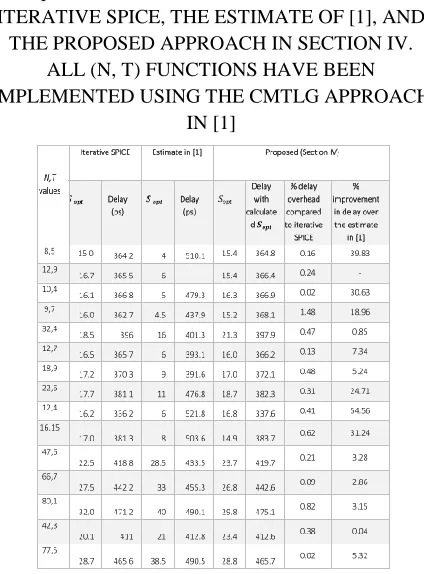
Tables II– IV show the point by point comes about that exhibit the prevalence of the Sopt ID technique in Section IV for all the three usage strategies. Specifically, Table II exhibits the outcomes when every (N, T) work is executed utilizing the CMTLG approach in [1], Table III introduces the outcomes when each capacity is actualized utilizing the CMTLG approach in [11], and Table IV when the capacities were actualized utilizing the approach in Section IV.
Sopt AND MINIMUM DELAY (IN PS) WITH ITERATIVE SPICE, THE ESTIMATE OF [1], AND
THE PROPOSED APPROACH IN SECTION IV. ALL (N, T) FUNCTIONS HAVE BEEN IMPLEMENTED USING THE CMTLG APPROACH
IN [1]
Table II concentrates on the CMTLG usage [1]. For this execution, we additionally looked at the effect of the proposed ideal size distinguishing proof technique in Section IV against another approach. In particular, Bobba and Hajj [1] evaluated the ideal sensor measure for a given estimation of N in a CMTLG usage to be around (N/2)μm. Notice that this strategy did not mull over the estimation of T. All the more essentially, the exhibited comes about demonstrate that this estimation here and there neglects to actualize the capacity effectively.
The accompanying blueprint the outcomes recorded in Table II. Section 1 records the (N, T) elements of Table I. Segment 2 records the base sensor estimate that was figured for each capacity utilizing the iterative SPICE approach, and the best watched entryway delay (in ps) by iterative SPICE is recorded in segment 3. Section 4 records the estimation of Sopt as recorded in [1], and the comparing entryway delay (acquired by SPICE) is appeared in segment 5 of Table II. Segment 6 gives the ideal sensor estimate utilizing the proposed strategy in Section IV, and segment 7
records the entryway delay (in ps) acquired by a SPICE reproduction. For the second capacity where (N, T) = (12, 9), the guess strategy in [1] brought about an erroneous execution, and this is signified by "−" in Table II.
The outcomes in segments 2 and 6 in Table II demonstrate that the sensor sizes by the proposed strategy and iterative SPICE are close for all the recorded capacities actualized with CMTLG. Conversely, the sensor measure evaluate in section 4 is regularly altogether different. Segments 3 and 7 demonstrate that for each capacity, the door delay when devouring iterative SPICE is practically indistinguishable to that returned by the proposed technique. Specifically, segment 8 demonstrates that for each actualized work with CMTLG, the door delay by our technique was close to 0.4% of the postponement for the sensor measure registered when devouring iterative SPICE strategy. Interestingly, section 9 of Table II demonstrates that the entryway delays by our strategy were substantially less (frequently more than 25% more) than the defers where the sensor measure was controlled by [1].
TABLE III
Sopt AND MINIMUM DELAY (IN PS) WITH ITERATIVE SPICE AND THE PROPOSED
APPROACH IN SECTION IV. ALL (N, T) FUNCTIONS HAVE BEEN IMPLEMENTED USING
Table III considers work usage utilizing the DCML strategy in [11]. In Table III, we look at the sensor distinguishing proof technique for Section IV with the tedious iterative SPICE strategy. Section 1 records the (N, T) elements of Table I, segment 2 records the base sensor measure that was figured for each capacity utilizing iterative SPICE, and segment 3 the best watched door delay (in ps) by iterative SPICE. Segment 4 gives the ideal sensor measure utilizing the proposed strategy in Section IV, and segment 5 records the particular door delay (in ps). Similar to the case for CMTLG usage, the outcomes in segments 2 and 4 demonstrate that the sensor estimate by the proposed technique is near the best sensor sizes by iterative SPICE for all the recorded capacities actualized with DCML. For each capacity actualized with DCML, segments 3 and 5 demonstrate that the entryway defer where the sensor estimate was dictated when devouring iterative SPICE is practically indistinguishable to the door postpone where the sensor measure was controlled by the proposed strategy in Section IV. All the more particularly, section 6 demonstrates that the door delay by our technique was close to 0.93% of the entryway delay by iterative SPICE.
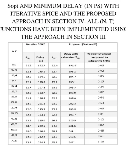
TABLE IV
Sopt AND MINIMUM DELAY (IN PS) WITH ITERATIVE SPICE AND THE PROPOSED
APPROACH IN SECTION IV. ALL (N, T) FUNCTIONS HAVE BEEN IMPLEMENTED USING
THE APPROACH IN SECTION III
Table IV expounds on work executions utilizing the proposed DCCML technique in Section III, and we demonstrate the effect of the sensor recognizable proof strategy for Section IV contrasted and iterative SPICE. Segment 1 records again all the (N, T) works in Table I. Segment 2 shows the base sensor measure for each capacity utilizing iterative SPICE, and section 3 the best watched door delay (in ps) by iterative SPICE. Segment 4 gives the ideal sensor estimate got with the proposed technique in Section IV, and segment 5 records the individual door delay (in ps). Just like the case for CMTLG and DCML executions, the outcomes in segments 2 and 4 demonstrate that the sensor sizes by the proposed strategy and iterative SPICE are close for all the DCCML usage. Segments 3 and 5 demonstrate that when the sensor estimate was figured when devouring iterative SPICE, it is constantly fundamentally the same as the defer when the sensor measure was immediately ascertained by the proposed technique in Section IV. Specifically, segment 6 demonstrates that for every one of the capacities the DCCML delay with the technique in Section IV was never over 1.15% of the entryway delay by iterative SPICE.
The outcomes in Tables II– IV obviously show that free of the present mode execution technique, the proposed diagnostic strategy in Section IV computes a sensor measure for which the door has for all intents and purposes ideal postponement. Subsequently, (3) in Section IV ought to be utilized to rapidly compute the transistor estimate for any (N, T) work under any present mode usage.
In the second piece of this area, the present mode usage in Section III is contrasted and the TLG current mode executions in [1] and [11] and in addition the conventional CMOS outlines concerning entryway delay (in ps) and also PDP, likewise alluded to as exchanging vitality (in fJ). The capacities in Table I were considered and the heap capacitance considered for every one of these capacities was set to 30 fF.
three-NAND, and inverter doors. Like the composed TLGs, least estimated transistors are considered as 240 nm.
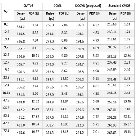
TABLE V
GATE DELAY AND SWITCHING ENERGY WITH THE CMTLG, DCML, DCCML (PROPOSED), AND STANDARD CMOS IMPLEMENTATIONS FOR
ALL (N, T) FUNCTIONS IN TABLE I
Table V abridges this near examination for the 15 diverse limit rationale works in Table I. Table V is partitioned into nine sections. Section 1 records the N and T estimations of the capacities. For each capacity, sections 2 and 3 demonstrate the door deferral and PDP for the CMTLG execution [1]. Sections 4 and 5 demonstrate the entryway delay and the PDP for the DCML usage [11]. Segments 6 and 7 demonstrate the entryway deferral and PDP for the proposed DCCML execution in Section III. At last, segments 8 and 9 demonstrate the door postponement and PDP acquired utilizing standard CMOS execution.
Watch that the proposed DCCML execution beat DCML and CMTLG for every one of the capacities, and for a few capacities the DCCML deferral and exchanging vitality were radically decreased. For instance, for work (22, 6) both the postponement and exchanging vitality were half of those acquired by the other two executions. Likewise,
sections 6 and 8 demonstrate that the DCCML delay was constantly not exactly in standard CMOS executions. The outcomes additionally demonstrate that the PDP is altogether less for the bigger capacities that have more than five information sources. Observe that the advantages in both the deferral and PDP increment as the capacities turn out to be more unpredictable. For instance, for work (N, T) = (80, 1) the postponement of our TL configuration is lessened by 45 ps, though the PDP of the CMOS execution is six times more than the proposed. The outcomes in Table V plainly demonstrate that the proposed DCCML strategy can be utilized to plan fast and exchanging vitality productive capacities.
VI. CONCLUSION
The presented analytical method has been proposed to identify quickly the transistor size in the sensor component of a current mode implementation that ensures very low gate delay (very close to the minimum) to optimize performance., independent of the current mode method used to implement the threshold logic function. It has been observed that the delay increases sub-linearly to the number of inputs of current mode TLG. This resulted to the design of current mode TLGs with large number of inputs whose delay is significantly less than traditional CMOS. A new current mode implementation method was also proposed that outperforms existing implementations both in gate delay as well as energy.
REFERENCES
[1] S. Bobba and I. N. Hajj, ―Current-mode threshold logic gates,‖ in Proc. IEEE ICCD, Sep. 2000, pp. 235– 240.
[2] T. Ogawa, T. Hirose, T. Asai, and Y. Amemiya, ―Threshold-logic devices consisting of subthreshold CMOS circuits,‖ IEICE Trans. Fundam. Electron., Commun. Comput. Sci., vol. E92-A, no. 2, pp. 436– 442, 2009.
[3] S. Muroga, Threshold Logic and Its Applications. New York, NY, USA: Wiley, 1971.
[5] S. Leshner, K. Berezowski, X. Yao, G. Chalivendra, S. Patel, and S. Vrudhula, ―A low power, high performance threshold logic-based standard cell multiplier in 65 nm CMOS,‖ in Proc. IEEE Comput. Soc. Annu. Symp. VLSI, Lixouri, Greece, Jul. 2010, pp. 210–215.
[6] M. Sharad, D. Fan, and K. Roy. (2013). ―Ultra-low energy, highperformance dynamic resistive threshold logic.‖[Online].Available:http://arxiv.org/abs/1308.467 2
[7] P. Celinski, J. F. López, S. Al-Sarawi, and D. Abbott, ―Low power, high speed, charge recycling CMOS threshold logic gate,‖ Electron. Lett., vol. 37, no. 17, pp. 1067–1069, Aug. 2001.
[8] S. Leshner and S. Vrudhula, ―Threshold logic element having low leakage power and high performance,‖ WO Patent 2009 102 948, Aug. 20, 2009.
[9] T. Shibata and T. Ohmi, ―A functional MOS transistor featuring gatelevel weighted sum and threshold operations,‖ IEEE Trans. Electron Devices, vol. 39, no. 6, pp. 1444–1455, Jun. 1992.
[10] V. Beiu, J. M. Quintana, and M. J. Avedillo, ―VLSI implementations of threshold logic—A comprehensive survey,‖ IEEE Trans. Neural Netw., vol. 14, no. 5, pp. 1217–1243, Sep. 2003.
[11] T. Gowda, S. Leshner, S. Vrudhula, and S. Kim, ―Threshold logic gene regulatory networks,‖ in Proc. IEEE Int. Workshop GENSIPS, Jun. 2007, pp. 1–4.
[12] A. K. Palaniswamy and S. Tragoudas, ―A scalable threshold logic synthesis method using ZBDDs,‖ in Proc. 22nd Great Lakes Symp. VLSI, 2012, pp. 307– 310.
[13] C. B. Dara, T. Haniotakis, and S. Tragoudas, ―Delay analysis for an N-input current mode threshold logic gate,‖ in Proc. IEEE Comput. Soc. Annu. Symp. VLSI (ISVLSI), Aug. 2012, pp. 344–349.
[14] A. K. Palaniswamy, T. Haniotakis, and S. Tragoudas, ―ATPG for delay defects in current mode threshold logic circuits,‖ IEEE Trans. Comput.- Aided Des. Integr. Circuits Syst., vol. PP, no. 99, pp. 1–1.
[15] A. Neutzling, J. M. Matos, A. Mishchenko, R. Ribas, and A. I. Reis, ―Threshold logic synthesis based
on cut pruning,‖ in Proc. ICCAD, Nov. 2015, pp. 494– 499.
[l6] K. Bernstein et. al., High speed CMOS design styles Boston, MA: Kluwer academic publishers, 1998.
[17] L. G. Heller et. al., ―Cascode voltage switch logic: A differential CMOS logic family,‖ in Proc. of ISSCC, 1984, pp.
[18] T. A. Groijohn and B. HoeWinger, ―Sample-set differential logic (SSDL) for complex high speed VLSI,‖ IEEE Journal of Solid State Circuits, vol. 21, no. 2, pp. 367-369, Apr. 1986.
[19] S.-L. Lu, ―Implementation of iterative networks with CMOS differential logic,‖ IEEE Journal of Solid State Circuits, vol. 23, no. 4, pp. 1013-10.17, Aug. 1988. (51 D. Somasekhar and K. Roy, ―Differential current switch logic: A low power DCVS logic family,‖ IEEE Journal of Solid State Circuits, vol. 31, no. 7, pp. 981-991, July 1996.
[20] H. Soeleman and K. Roy, ―Digital CMOS logic operation in the sub-threshold region,‖ in Proc. of GLS-VLSI, Mar. 2000.
[21] J. Von Neumann, ―Probabilistic logics and the synthesis of reliable organisms from unreliable components,‖ Automatica studies, C. E. Shannon and J. McCarthy, Eds., Princeton, NJ: Princeton Univ. Press, 1956, pp. 43-98.