Implementation of Space Vector Modulation
for Two Level Inverter and its Comparison
with SPWM
Simran Bhalla
1, Dr.Jagdish Kumar
2PG Student, Dept. of Electrical Engg. , Punjab Engineering College, Chandigarh,Punjab, India1
Associate professor, Dept. of Electrical Engg., Punjab Engineering College, Chandigarh, Punjab, India2
ABSTRACT: With increasing research and advancement in solid-state power electronic devices and microprocessors, various inverter control techniques employing pulse-width-modulation (PWM) are becoming popular esp. in AC motor drive applications. The most commonly used techniques are Sine PWM and Space vector modulation (SVPWM). SVPWM is considered to be superior to the SPWM because of better DC bus utilization. This paper focuses on step by step development of MATLAB/SIMULINK model of SVPWM.Firstly model of a three-phase VSI is discussedbased on space vector representation. Nextsimulation model of SVPWM is obtained using MATLAB/SIMULINK. Finally the simulation results of SVM are compared with SPWM.
KEYWORDS:Cascaded Multi-level Inverters, Space Vector Modulation, Sine PWM,Matlab/Simulink.
I.INTRODUCTION
For a long period, carrier-based PWM methodswere widely used in most applications. Theearliest modulation signals for carrier-based PWM [4]are sinusoidal. The use of an injected zero-sequence signal for a three-phase inverter [5] initiated the research on sinusoidal carrier-based PWM. Different zero-sequence signals lead to different non-sinusoidal PWM modulators. Compared with non-sinusoidal three-phase PWM, non-non-sinusoidal three-phase PWM can extend the linear modulation range for line-to-line voltages. Space-vector modulation has become one of the most important PWM methods for three-phase converters.
There is no single PWM method that is the best suited for all applications and with advances in solid-state power electronic devices and microprocessors, various pulse-width modulation (PWM) [3-5] techniques have been developed for industrial applications .The most widely used PWM schemes for three-phase voltage source inverters are carrier-based sinusoidal PWM and space vector PWM (SVPWM).Theoutput voltage per phase for a sinusoidal PWM carrier-based three phase converter is limited to 0.5Vdc (peak value) and the line-to-line RMS voltage is 0.612Vdc.SVM is another
direct digital PWM technique proposed in 1982 [2, 6]. It has become a basic power processing technique in three-phase converters [5]. SVM based converter can have a higher output voltage output at 0.707Vdc (Line-to-line, RMS).
The classic SVM strategy, first proposed by Holtz [8, 9] and Van der Broeck [6] Reviewing the literature it can be concluded that SVPWM has certain advantages over SPWM [1, 6, 7]. They are:
The output voltage is about 15% more in case of SVPWM as compared to SPWM.
The current and torque harmonics produced are much less in case of SVPWM.
The maximum peak fundamental magnitude of the SVPWM technique is about 90.6% of the inverter capacity in linear modulation range.
II.TWO LEVEL INVERTER
The circuit in Fig.1 demonstrates the foundation of a two-level three phase voltage source converter. It has six switches (S1-S6) and each of these is represented with an IGBT switching device. A, B and C represents the output for the phase shifted sinusoidal signals. Depending on the switching combination the inverter will produce different outputs, creating the two-level signal (+Vdc and -Vdc).
Fig.1 Basic diagram of two level three phase inverter
The switches 1,3 and 5 are the upper switches and if these are 1 (separately or together) it turns the upper inverter leg ON and the terminal voltage (Va, Vb, Vc) is positive (+Vdc). If the upper switches are zero, then the terminal voltage is
zero.
The lower switches are complementary to the upper switches, so the only possible combinations are the switching states: 000, 001, 010, 011, 100, 110, 110, and 111.
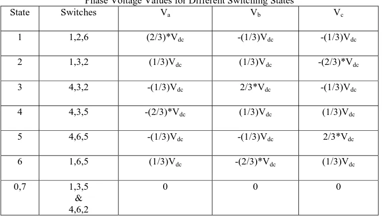
Table 1
Phase Voltage Values for Different Switching States
State Switches Va Vb Vc
1 1,2,6 (2/3)*Vdc -(1/3)Vdc -(1/3)Vdc
2 1,3,2 (1/3)Vdc (1/3)Vdc -(2/3)*Vdc
3 4,3,2 -(1/3)Vdc 2/3*Vdc -(1/3)Vdc
4 4,3,5 -(2/3)*Vdc (1/3)Vdc (1/3)Vdc
5 4,6,5 -(1/3)Vdc -(1/3)Vdc 2/3*Vdc
6 1,6,5 (1/3)Vdc -(2/3)*Vdc (1/3)Vdc
0,7 1,3,5 & 4,6,2
0 0 0
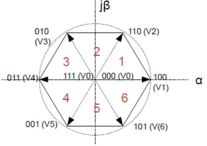
This means that there are 8 possible switching states, for which two of them are zero switching states and six of them are active switching states. These are represented by active (V1-V6) and zero (V0) vectors in Fig.2. The zero vectors are
Table 2
Phase Voltage Space Vectors
State Phase voltage space vectors
1 (2/3)Vdc
2
(2/3)Vdc𝑒
𝑗 (𝑝𝑖
3)
3
(2/3)Vdc𝑒
𝑗 (2𝑝𝑖
3)
4 (2/3)Vdc𝑒𝑗 (𝑝𝑖 )
5
(2/3)Vdc𝑒
𝑗 (4𝑝𝑖
3)
6
(2/3)Vdc𝑒
𝑗 (5𝑝𝑖
3)
0,7
(2/3)Vdc𝑒
𝑗 (2𝑝𝑖
1)=0
III. SPACE VECTOR MODULATION
SVPWM is accomplished by rotating a reference vector around the state diagram, which is composed of six basic non-zero vectors forming a hexagon. The reference is sampled at fixed interval and is formed using the voltage vectors of the particular sector in which reference lies along with zero vectors.
Fig. 2 Space vector diagram
The three phase instantaneous voltages are:
𝑉𝑎 = 𝑉 sin( 𝜃𝑡)
𝑉𝑏= 𝑉 sin(𝜃𝑡 + 2(
𝑝𝑖 3))
𝑉𝑐= 𝑉 sin(𝜃𝑡 + 4
𝑝𝑖 3 )
The magnitude and angle of this vector can be calculated with Clark's Transformation:
𝑉𝑟𝑒𝑓 = 𝑉𝛼+ 𝑗𝑉𝛽 =
2
3∗ (𝑉𝑎+ 𝛼𝑉𝑏+ 𝛼
2𝑉
𝑐)
Where α is given by:
𝛼 = 𝑒𝑗 2𝑝𝑖 /3
Vector is:
Vref = 𝑉
𝛼2+ 𝑉
𝛽2θ = tan
−1(𝑉
𝛽/𝑉
𝛼)
Using this angle we determine the sector in which Vref lies and corresponding to that sector we determine the voltage
vectors with which we have to form Vref.
Table 3 Sector Determination
Sr. No. Angle Range Sector
1. 0 to 60 1
2. 6 to 120 2
3. 120 to180 3
4. -180 to -120 4
5. -120 to-60 5
6. -60 to 0 6
These discrete positions are shown in the Figure 2.
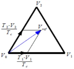
Next step is to calculate the dwell times or time for which we have to provide voltage vectors, so as to generate the Vref
at that particular point of time. Vref can be found with two active and one zero vector. For sector 1 (0 to pi/3), Vref can
be generated with V0, V1 and V2 as shown in fig.3. Vref in terms of the duration time can be considered as:
Vref *Ts= V1*T1+V2*T2+ V0*T0
Where Ts is the sampling time (3.3 *104sec) and T1, T2 andT0 are the time periods for which V1, V2 and V0 are applied
for particular sample.
𝑇1= (𝑇𝑠∗ 3 ∗ 𝑉𝑟𝑒𝑓 ∗ sin
𝑝𝑖
3 − 𝜃 )/𝑉𝑑𝑐
𝑇2= (𝑇𝑠∗ 3 ∗ 𝑉𝑟𝑒𝑓 ∗ sin 𝜃 )/𝑉𝑑𝑐
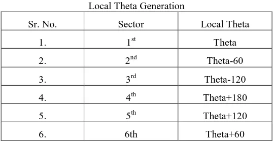
To make calculations easy generate local theta i.e. the Vrefin any sector can be supposed to be layingin first sector and
voltage vectors as per the sector can be applied using time calculation of first sector. This eliminates the process of calculating dwell times separately for each sector.
Table 4 Local Theta Generation
Sr. No. Sector Local Theta
1. 1st Theta
2. 2nd Theta-60
3. 3rd Theta-120
4. 4th Theta+180
5. 5th Theta+120
6. 6th Theta+60
IV. SEQUENCING OF SWITCHING STATES
Each switch has it switching information depending on where the reference vector is located. This paper presents two different ways of sequencing of switching states:
Using three switching states ( using only one zero state-SVM1)
Using four switching states ( using both zero states-SVM2) The switching logic for both ways is tabulated below.
Table 5
Switching Logic Using Three Switching States
Sr. No. Condition Voltage vector to be applied
1. T1>Ts V1
2. T1<Ts <T1+T2 V2
3. T1+T2< Ts V0
Here V1 V2 used are decided according to the sector in which Vref lies and V0 is always taken to be (000).This is
asymmetric type of switching.
Table 6
Switching Logic Using Four Switching States
Sr. No. Condition Voltage vector to be applied
1. T0/4> Ts V0
2. T0/4< Ts<T0/4+ T1/2 V1
3. T0/4+ T1/2< Ts< T0/4+ T1/2+ T2/2 V2
4. T0/4+ T1/2+ T2/2< Ts< T0/4+ T1/2+ T2/2+ T0/2 V7
5. T0/4+ T1/2+ T2/2+ T0/2<Ts< T0/4+ T1/2+ T2/2+ T0/2+ T2/2
6. T0/4+ T1/2+ T2/2+ T0/2+ T2/2 <Ts< T0/4+T1/2+ T2/2+ T0/2+ T2/2+ T1/2
V1
7. T0/4+ T1/2+ T2/2+ T0/2+ T2/2+ T1/2<Ts< T0/4+ T1/2+ T2/2+ T0/2+ T2/2+ T1/2+ T0/4
V0
This is symmetric type of switching also known as seven segment switching.
The pulses are generated using timing sequence subsystem, voltage vectors subsystem and multiport switch. Multiport switch has three outputs; using not gates six pulses are generated that are further given to the inverter switches as explained above.
V. SIMULATION RESULTS AND DISCUSSIONS
Following are steps involved in the implementation of SVM for two-level inverters:
The first block is used to generate three-phase sinusoidal input voltages with variable frequency, amplitude, direction, and DC bus voltage. The three signals are displaced by 120 degree from each other.
The three-phase voltages are then converted to two-phase α-β voltages as described above, and further converted to polar form.
Next block is for sector determination and local theta calculation, the angle calculated above is used for the same.
Then calculate T1, T2 and create subsystem- sequencing of switching states. Next is determination of switching states in the subsystem named as voltage vector.
Last step is Realization of switching states (multi-port switch is used). The multiport switch has three outputs, so using three not gates 6 individual gate pulses are derived that are to be given to the two level inverter.
Sampling time used is 3.33*104, to take samples, sampling – hold circuit is used.
Simulink model specifications and FFT results:
Inverter input voltage = 100 V, modulation Index = .75, R-L Load (R=1 Ohm, L=1 Henry), frequency=50Hz.
The simulation waveforms for two level inverter using space vector modulation technique are shown below:
Fig.4. Line voltageVab
The line voltage has two levels and the peak value is as high as DC bus voltage i.e. 100V. As it is symmetrical even harmonics are absent, also the triplen harmonics are absent in line voltage.
0 0.005 0.01 0.015 0.02 0.025 0.03 0.035 0.04 0.045 0.05
-150 -100 -50 0 50 100 150
Time
L
in
e
V
o
lt
a
g
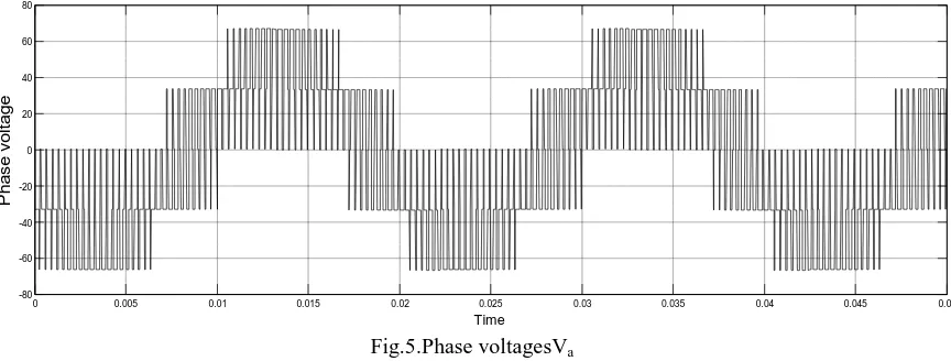
Fig.5.Phase voltagesVa
Fig.5 shows the phase voltage of two level inverter. The peak value here is 2/3 rd of the DC bus voltage.
Fig6. Load current of three phases
The waveform of load current shows that load currents are almost sinusoidal , thus has very small content of harmonics.
Table 7 SPWM Results
Sr. No. Modulation technique
Line Voltage Phase Voltage Load Current
Fundamental THD Fundamental THD Fundamental THD
1. SPWM 65.08 V 97.79% 37.60 V 97.79% 11.4A 1.05%
2. SVM-1 87.37V 66.80% 50.45 V 66.82% 15.31 1.09%
3. SVM-2 86.23V 69.42 % 49.79V 69.35 % 15.11 0.80%
VI.CONCLUSION
Simulation results reported in this paper confirm that the developed model generates waveforms with complete symmetry. Amplitude of line to line voltage is as high as DC bus voltage in SVM technique. It is concluded from the tabular data that Inverter employing SVM has lower THD and higher fundamental component as compared to the inverter with SPWM. Among three switching state and four switching state technique, though THD of four switching inverter increases slightly, but lower order harmonics are reduced. The current harmonics are much less in inverter employing SVM with four switching states.
0 0.005 0.01 0.015 0.02 0.025 0.03 0.035 0.04 0.045 0.05
-80 -60 -40 -20 0 20 40 60 80 Time P h a se vo lt a g e
0 0.005 0.01 0.015 0.02 0.025 0.03 0.035 0.04 0.045 0.05
REFERENCES
[1] Atif Iqbal, AdoumLamine, ImtiazAsharf and Mohibullah, “MATLAB/SIMULINK model of space vector pwm for three phase voltagesource inverter,” in Proc UPEC, 2006, p. 1096-1100.
[2] Xiang Shaobang and HhaoKe-You, “Research on a Novel SVPWM Algorithm ,” in Proc. of 2007 Second IEEE Conference on Industrial Electronics and Applications p.1869-187.
[3]D. G. Holmes and T. A. Lipo, Pulse width modulation for power converters: principles and practice. Wiley-IEEE Press, 2003, vol. 18. [4] S. R. Bowes, “New sinusoidal pulsewidth modulated inverter,” Proc. Inst. Elect. Eng., vol. 122, pp. 1279–1285, 1975.
[5] J. Holtz, “Pulse width modulation for electronic power conversion,” Proc. IEEE, vol. 82, pp. 1194–1214, Aug. 1994.
[6] H. W. v. d. Brocker, H. C. Skudenly, and G. Stanke, “Analysis and realization of a pulse width modulator based on the voltage space vectors,” inConf. Rec. IEEE-IAS Annu. Meeting, Denver, CO, 1986, pp. 244–251.
[7] O. Ogasawara, H. Akagi, and A. Nabel, “A novel PWM scheme of voltage source inverters based on space vector theory,” in Proc. EPE EuropeanConf. Power Electronics and Applications, 1989, pp. 1197–1202.
[8] J. Holtz, P. Lammert and W. Lotzkat, “High speed drive system with ultrasonic MOSFET PWM inverter and single-chip microprocessor control,” IEEE Transactions on Industry Applications, vol. 23, pp. 1010-1015,1987.