Design and Analysis of auxiliary circuits ZCS based full- bridge
Converter to single phase induction drive applications
Sakinala Govardhan, Thogaru Venkateshwarlu
Assistant Professor, Department of EEE, CITS –Warangal
Research Scholar, Depaert of EEE.
ABSTRACT:A new soft switching pulse-width-modulated (PWM) fly back dc/dc converter with a simple auxiliarycircuit is proposed. This isachieved by using two very simple active auxiliary circuitsoneactive, the other passive. The outstanding featureof the new converter is that it allows its main power switchesto operate with zero current switching (ZCS) and with fewer conductionlosses than conventional full-bridge converters.By adding this auxiliary circuit to the conventional pulse width modulation isolated fly back converter,Is isolated with the inducation motor applications.proposed techniques for higher power dc–dc full-bridge converterswith IGBTs, including resonant techniques, ZCS-PWMtechniques with active auxiliary circuits, passive techniques,ZVZCS techniques, and techniques that require the use of reverseblocking diodes. Experimental results obtained from all power semiconductor devices are soft switched. In addition, the proposed converter frequency is constant and has no additional current stress in the main switch in comparison with conventional ones. In the Simulation and experimental results justify the theoretical analysis.
...
I.INTRODUCTION
NEW techniques are proposed in order to decrease witching losses and to increase power density in dc–dc converters at high power and frequencies [1]–[4]. The applications of soft-switching methods are expanding. The most remarkable method in high-power isolated applications is Phase Shifted (PS) Zero Voltage Switching (ZVS) method, which provides all of the switches to operate with ZVS without any additional auxiliary switches. The parasitic capacitance energy is discharged by the leakage inductance, and the MOSFET turns on with zero voltage transition (ZVT). Insulated gate bipolar transistor (IGBT) is preferred over MOSFET at high voltage and high-power levels in industrial applications. Low RDSONMOSFETs are quite expensive compared to the IGBTs with equivalent current and voltage ratings. The choice of IGBT over MOSFET is mandatory due to nonavailability of high voltage and high-current MOSFET devices in some applications. An external snubber capacitor is connected in parallel to each IGBT in order to
light loads, and high-voltage peaks and oscillations at the output diodes, and increment in the conduction losses because of the primary current flowing in the freewheeling
interval. It is possible to encounter many studies in the literature about these converters and solution for the problems [5]–[26].
II.CIRCUIT DIAGRAM
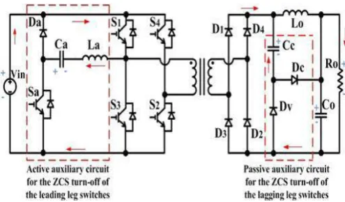
Fig.1.Circuit Diagram Of Dc-Dc Converter
A new ZCS-PWM full-bridge converter is proposed in this paper. The outstanding feature of the new converter is that itallows its main power switches to operate with ZCS and with fewer conduction losses than conventional full-bridge converters.This is achieved by using two very simple active auxiliary circuits—one active with a switch that can turn on and off with ZCS and one passive that consists of a few passive components.The paper presents the new converter and then discusses its operation, steady-state characteristics and design. Experimental results obtained from a converter prototype are presented to validate the converter’s performance and the concepts presented in the paper.A new ZCS-PsWM full-bridge converter is proposed in this paper. The outstanding feature of the new converter is that it allows its main power switches to operate with ZCS and with fewer conduction losses than conventional full-bridge converters. This is achieved by using two very simple active auxiliary circuits—one active with a switch that can turn on and off with ZCS and one passive that consists of a few passive components.The paper presents the new converter and then discusses its operation, steady-state characteristics and design. Experimental results obtained from a converter prototype are presented to validate the
converter’s performance and the concepts presented in the paper.
III.CONVERTER OPERATION
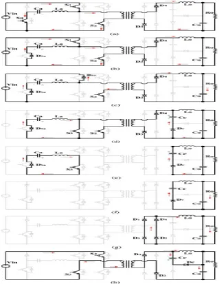
The proposed converter is shown in Fig. 1. It operates like a ZVZCS-PWM converter except that the auxiliary circuit is activated whenever the main power switches in the leadingleg to which it is attached are about to turn off. It should be noted that in this diagram, as in other circuit diagram present in this paper, the transformer leakage inductance is not shown as a separate element, but is assumed to be a part of the transformer.Equivalent circuit diagrams of the modes of operation that the proposed converter goes through during a half switching are shown in Fig. 2 and ideal converter waveforms are shown in Fig. 3.
It should be noted that in Fig. 3, a current waveformsuch as IS1 shows the current flowing through a switch (positive part of the waveform) and its body diode (negative part of thewaveform). Moreover, the ISa
waveform is also the waveformfor ILa and ICa
as ISa = ILa = ICaandV_Ca on the VCa
waveformcan be considered to be equal to the input voltage.
value.
When the device wakes-up, it will continue from this state.In [7], an auxiliary circuit which includes twoMOSFETs and a serial inductance is proposed. The inductance current is increased before the IGBT devices on the lagging leg are turned off. The ZVS conditions of the FB converter are improved,
but the losses in the auxiliary circuit reduce the efficiency. The auxiliary circuit does not operate with soft switching. Main IGBTs are subjected to the current stress before turn off and this increases the switching losses in the turn-off process. Theproposed method is not preferred due to low efficiency, high cost, and control difficult.
Fig. 2.Equivalent circuit for each mode of operation.
IV.MAIN FEATURES AND DESIGN PROCEDURE
In this section, the design procedure of the proposedconverter is given. The component values forimplementing the converter are determined according to the design procedure. A Selection of the Boundary Current Ia.The boundary current level Ia . The proposed converter is shown in Fig.
valued snubber capacitors are connected at the lagging leg. These capacitors provide ZVS operation at light loads and improve the turn-offbehavior of the IGBT until a current level. In the proposed converter, auxiliary circuit is operated only at high-output currents. By means of the auxiliary circuit, high value capacitors are connected to the lagging leg and the turnoff performance of the lagging leg
switches is improved. The IGBTs used in the auxiliary circuit operate under soft-switching conditions. The conduction loss of the auxiliary switches is very low because they conduct current for a very short time. The operation of the auxiliary circuit starts when primary current IP is larger than boundary current level Ia.
VI.CONCLUSION
A new ZCS-PWM full-bridge converter is imposed with induction motor drive applications is proposed in this paper. The outstanding feature of the new converter is that it allows its main power switches to operate with ZCS, Efficiency comparison results.Few conduction losses than conventional full-bridge converters. This is achieved by using a very simple active auxiliary circuit and a ZVZCS technique so that the converter has all the advantageous features of ZVZCS converters but with ZCS operation for all the converter switches so that they can all beIGBT devices, MOSFET devices. which helps reduce component cost. ZCS-PWM techniques withactive auxiliary circuits, passive techniques, ZVZCS techniques, and techniques that require the use of reverse blocking diodes. Experimental results will obtained. converter prototype confirm the feasibility of the converter and show that the active auxiliary circuit results in a maximum efficiency improved. compared to the conventional ZVZCS converter due to the elimination of leading leg turn-off losses due the inducation motor drive applications.
REFERENCES
[1] C. Liu, B. Gu, J. Lai, M. Wang, C. Zheng, Y. Ji, and P. Sun, ―Highefficiency hybrid full-bridge–half-bridge converter with shared ZVS lagging leg and dual outputs in series,‖ IEEE Trans. Power Electron., vol. 28, no. 2, pp. 849–861, Feb. 2013.
[2]K. Jin, Y. Sun, M. Xu, D. Sterk, and F.C. Lee, ―Integrated magnetic selfdriven ZVS nonisolated full-bridge converter,‖ IEEE Trans. Ind.Electron.,
vol. 57, no. 5, pp. 1615–1623, May 2010. [3] X. Zhang, W. Chen, X. Ruan, and K. Yao, ―A novel ZVS PWM phaseshifted full-bridge converter with controlled auxiliary circuit,‖ in Proc.IEEE APEC, Feb. 2009, pp. 1067–1072.
[4] I. Lee and G. Moon, ―Soft-switching
dc/dc converter with a full ZVS range and reduced output filter for high-voltage applications,‖ IEEE Trans.Power Electronics, vol. 28, no. 1, pp. 112–122, Jan. 2013.
[5] W. Chen, X. Ruan, and J. Ge, ―A novel full-bridge converter achieving ZVS over wide load range with a passive auxiliary circuit,‖ in Proc. IEEEECCE, Sep. 2010, pp. 1110–1115.
[6] D. Sterk, M. Xu, and F.C. Lee, ―High frequency ZVS self-driven fullbridge using full integration of magnetics,‖ in Proc. IEEE APEC, 2010,
pp. 1210–1216.
[7] Z. Chen, M. Chen, F. Ji, and J. Li, ―Analysis and implementation of a novel full-bridge ZVS converter with adaptive auxiliary circuit,‖ in Proc.IEEE IECON, Nov. 2010, pp. 358–363.
[8] H. L. Do, ―Improved ZVS Dc–dc converter with a high voltage gain and a ripple-free input current,‖ IEEE Trans. Circuits Syst., vol. 59, no. 4, pp. 846–853, Apr. 2012.
[9] J. Sun, X. Ding, M. Nakaoka, and H. Takano, ―A novel series resonant ZCS full bridge three-level dc–ac inverter,‖ in Proc. IEEE APEC, 2008, pp. 419–425. [10] W. Huai, S. Qian, H. Chung, S.
Tapuchi, and A. Ioinovici, ―Series resonant ZCS-PFM DC–DC converter with multistage rectified voltage
multiplier
and dual-mode PFM control scheme for medical-use high-voltage X-ray power generator,‖ IEEE Trans. Electric Power Appl., vol. 147, no. 6, pp. 527–534, Aug. 2000.
[11] W. Chen, Y. Gu, and Z. Lu, ―A novel three Level full bridge resonant dc–dc converter suitable for high power wide range input applications,‖ in Proc. IEEE APEC, Feb./Mar. 2007, pp. 373–379.
[12]M.S. Agami and P. Jain, ―A new full bridge three level resonant single stage AC/DC converter,‖ in Proc. IEEE PESC, Jun. 2007, pp. 2699– 2704.
[13]W. Huai, S. Qian, H. Chung, S. Tapuchi, and A. Ioinovici, ―A ZCS currentfed full-bridgePWMconverter with self-adaptable soft-switching snubber
[14] K. Fathy, T. Doi, K. Morimoto, H. Lee, and M. Nakaoka, ―A novel soft-switching PWM full-bridge DC/DC converter with DC busline series switch-parallel capacitor edge resonant snubber assisted by highfrequency transformer leakage inductor,‖ in Proc. IEEE IPEMC, Aug. 2006, pp. 1–5. [15] K. Suzuoka, S. Moisseev, L. Gamage, K. Soshin, K. Nishida, and M. Nakaoka, ―Boost transformer linked full bridge soft-commutation DC–DC power converter with secondary-side phase-shifted PWM rectifier switches,‖ in Proc. IEEE IECON, Nov. 2003, pp. 49–54.
[16] K. Jin and X. Ruan, ―Hybrid full-bridge three-level LLC resonant converter— A novel DC–DC converter suitable for fuel-cell power system,‖ IEEE Trans. Ind. Electron., vol. 53, no. 5, pp. 1492–1503, Oct. 2006.
[17] X. Sun, J. Liu, X. Jin, and W. Wu, ―High power high frequency zero current transition full bridge DC/DC converter,‖ in Proc. IEEE APEC, Feb. 1998, pp. 823– 828.
[18]Muruganandam, M. and Madheswaran, M. ―Stability Analysis and Implementation of Chopper fed DC Series Motor with Hybrid PID-ANN Controller‖ Published in International Journal of Control, Automation and Systems, Springer, Volume 11, Issue 5, October 2013. ISSN: 1598-6446 (Print) 2005-4092 (Online)
[19]M. Muruganandam, M. Madheswaran, ―Experimental verification of chopper fed DC series motor with ANN controller‖ Published in International Journal of Frontiers of Electrical and Electronic Engineering in China, (Springer Publication) Volume 7, Issue 4, December 2012, pp 477-489. ISSN: 2095-2732 (print) 1673-3584 (Online)