5-Step and 6-Step Nested-Current-Mirror
Rail-to-Rail Output Single-Stage Amplifier with
Enhancements of DC Gain, GBW and Slew Rate
Geethumol K K1, Premanand B2
PG Scholar [VLSI & ES], Dept. of ECE, Government Engineering College, Idukki, Kerala, India1 Assistant Professor, Dept. of ECE, Government Engineering College, Idukki, Kerala, India2
ABSTRACT: For better performance, rail-to-rail output single-stage amplifiers are a potential replacement of their multi-stage counterparts, especially for display applications that entail massive buffer amplifiers in their column drivers. This paper describes a nested-current-mirror (NCM) technique for a single-stage amplifier to achieve high DC gain, gain-bandwidth product (GBW) and slew rate (SR). NCM technology is customizable for different mirror steps, and sub mirror ratios, to balance the performance metrics while preserving a rail-to-rail output swing. NCM amplifier can mitigate the fundamental power-efficiency limit set by the basic differential-pair (DP) amplifier. Two prototypes, 5-step and 6-step NCM amplifiers, were designed and analyzed in 0.18 µm CMOS for systematic comparison with the 3-step and 4-step NCM amplifier. 5-step NCM can provide 91 dB DC gain and 0.137–0.424 MHz GBW over 0.25 – 1 nF with >700 phase margin (PM). 6-step NCM design attaining 98 dB DC gain and 0.397–0.841 MHz GBW over 0.45– 1 nF with >750 PM.
KEYWORDS: DC gain, GBW, slew rate, nested current mirror, effective transconductance(GM,eff), mirror factor(K) I.INTRODUCTION
Low-temperature polysilicon (LTPS) LCD panels consist of thousands of buffer amplifiers in their column drivers. The area and power budgets of each buffer amplifier are very important because these factors determine the market pressure on cost and display quality [1]. Now-a-days multi-stage amplifiers dominate those applications owing to their key advantages of high DC gain and rail-to-rail output swing. Classical single-stage amplifiers were not commonly used in such application due to their limited capability in most metrics. So it is beneficial to revisit the fundamental limits of single-stage amplifiers and find a solution.
Most single-stage amplifiers suffer from a tight tradeoff between its power and performance. Telescopic amplifiers feature a GBW-to-power efficiency as high but sacrifice output swing. Folded cascode amplifiers partially surmount such swing limit, but at the expense of power. For LCD column drivers, current-mirror amplifiers are favored for their rail-to-rail output swing, and provide an extra design flexibility via adjusting the mirror ratio, K. A large K benefits most performance metrics (i.e., effective transconductance (GM,eff), GBW and SR),but at the expense of noise and phase
margin (PM). This paper introduces a nested-current-mirror (NCM) single-stage amplifier to advance its GBW-to-power/area efficiency and CL drivability beyond the multi-stage designs, while preserving a rail-to-rail output swing.
This nested-current-mirror (NCM) single stage amplifier can alleviate the tight performance tradeoffs in conventional single-stage amplifier topologies. Current-mirror factor K offers a freedom to leverage the various performance metrics such as effective transconductance, output resistance, gain-bandwidth product and slew rate. The prototyped 5-step and 6-step NCM amplifiers achieve favorable performances with respect to 3-step and 4-step NCM amplifiers.
II. NCM SINGLE-STAGE AMPLIFIER SYSTEM MODEL
allocated to the 1st mirror with a small K1. To increase SR, most of the current can be assigned to the second-last mirror
with enlarged KN-1 and KN. Indeed, the mirror stages and ratios of the NCM are only limited by the PM and transistor
mismatches. Thus, the DC gain of the NCM can be as high as that of a folded-cascode amplifier, but without the output swing penalty. Moreover, unlike the folded-cascode and current-mirror amplifiers, cutting the current of the output stage does not essentially degrade SR.
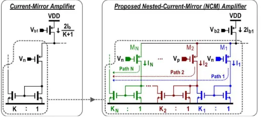
Fig. 1.Development of the NCM amplifier from the current-mirror amplifier.
Figure 1 shows the development of NCM amplifier from current mirror amplifier. Here the biasing current Ib1 is
distributed to the left N divided differential pair(DP) transistors and these transistors are alternately connected to Vp and Vn . These DP transistors outputs are combined via N nested current mirrors with different mirror ratio. Since these DP transistors are located in the signal path all those transconductance are contributed to an effective transconductance GM, eff. Correct selection of the mirror ratio have great influence on the performance matric.
The number of step is a design parameter. We show below 5-step and 6-step NCM design as they can provide appreciable gain, GBW and slew rate.
III. FIVE-STEP NCM AMPLIFIERS
Figure 2: Schematic of 5-step NCM
Figure 2 shows the schematic of a 5-step NCM amplifier. The DP transistors are split into M1 to M5. Their outputs are
summed via the NCM mirrors realized by M6 to M15. M16 collects the output of the left, to form the single-ended
output together with M15. To show how the mirror ratios K1 to K9 contribute to the effective transconductance
(GM,NCM5), GBW, DC gain and SR quantitative analyses are conducted, and they are valid for both single-ended output
and differential output implementations.
, =
× (2 + 1)
The GM,NCM5 is mainly determined by the product of K9 and K8×(K7 + K6 )/K7 with a given sum of K1 to K9. Since the
product is readily sized to be much higher than the sum, GM,NCM5is significantly boosted. The DC gain of the 5-step
NCM amplifier is expressed as the product of GM,NCM5and RO,NCM5. In addition to GM,NCM5 that already considerably
improves its DC gain RO,NCM5 is also enhanced over that of the DP amplifier, and can be represented by
, =
∑ + 1
× || (2)
The gain enhancement seen in RO,NCM5 is attributed to substantial bias current reduction in the output stage in
comparison with that of the DP amplifier. Thus, an overall DC gain enhancement over the DP amplifier can be observed. SR determines the amplifier's settling performance. Suppose a large negative step appears at Vp, it follows that the second-last mirror turns off. Consequently, almost all the current in M5 is directed into M14 and amplified by
the 5th mirror to discharge CL. Similar analyses can be applied when there is a large positive input step occurring at Vp,
resulting in a symmetric SR expressed by
= × ( + 1)
∑ + 1 ×
2
(3)
If numerator > denominator the SR of the proposed amplifier increases that of the DP amplifier, which can be realized by selecting relatively large K8 and K9.
IV. DESIGN AND STABILITY ANALYSIS OF 5-STEP NCM
Design : Mirror factors (K) selected for the circuit design can be mention as K1 = 4, K2 = 12, K3 = 2, K4 = 6, K5 = 4, K6
= 9, K7 = 3, K8 = 18, K9 = 2. For the 5-step NCM, the total bias current (3 µA) is divided into 120 unit-current (Iu = 25
nA). To leverage the key metrics, the 1st mirror (M6 to M7) uses a small ratio of only 3 (K1 = 4 and K2 = 12). The 2nd
mirror (M8 to M9) draws less current under a larger ratio of 3 (K3 = 2 and K4 = 6) to boost the DC gain and GBW, as
they contribute less noise. Also, a larger K8 enhances the SR. The 3rd mirror (M10 to M11) is assigned the ratio of 2 (K5 =
4 and K6 = 9 ). The 4th mirror (M12 to M13) is assigned the ratio of 6 (K7 = 3 and K8 = 18 ). The 5th mirror (M14 to M15)
is assigned the ratio 2 (K9 = 2) to benefit the SR and GM,NCM5. Substituting these values into the DC gain, GBW and SR
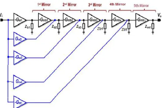
The equivalent small-signal diagram of the 4-step NCM amplifier is shown in Figure 3. Gm1, Gm2, Gm3, Gm4 and Gm5 are
the transconductances of M1-5 respectively while Zb1, Zb2, Zb3, Zb4 and Zb5 correspond to the input impedances of the 1st
to 5th mirrors. The transconductances of the transistors in the five mirrors are respectively represented by Gmb1-5, while
Zout models the output impedance that includes CL.
V. SIX-STEP NCM SINGLE-STAGE AMPLIFIER
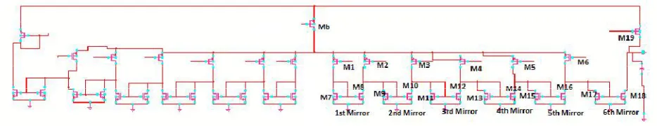
Figure 4: The schematic of the 6-step NCM amplifier
Figure 4 shows the schematic of a 6-step NCM amplifier. The DP transistors are split into M1 - M6. Their outputs are
summed via the NCM mirrors realized by M7 - M18. M19 collects the output of the left, to form the single-ended output
together with M18. To show how the mirror ratios K1 to K11 contribute to the effective transconductance (GM,NCM6),
GBW, DC gain and SR quantitative analyses are conducted, and they are valid for both single-ended output and differential output implementations.
, =
× (2 × ×
× +
×
+ + 1)
∑ + 1 × (4)
Since the product is readily sized to be much higher than the sum, GM,NCM6is significantly boosted.
The DC gain of the 4-step NCM amplifier is expressed as the product of GM,NCM6 and Ro,NCM6. In addition to GM,NCM6
that already considerably improves its DC gain, Ro,NCM6 is also enhanced over that 3-step and 4-step NCM, and can be
represented by
, =
∑ + 1
× || (5)
The gain enhancement seen in Ro,NCM6 is attributed to substantial bias current reduction in the output stage in
comparison with that 3-step and 4-step NCM.
SR determines the amplifier's settling performance. Suppose a large negative step appears at Vp, it follows that the second-last mirror turns off. Consequently, almost all the current in M6 is directed into M17 and amplified by the last
mirror to discharge CL. Similar analyses can be applied when there is a large positive input step occurring at Vp,
resulting in a symmetric SR expressed by
= × ( + 1)
∑ + 1 ×
2
(6)
VI. DESIGN AND STABILITY ANALYSIS OF 6-STEP NCM
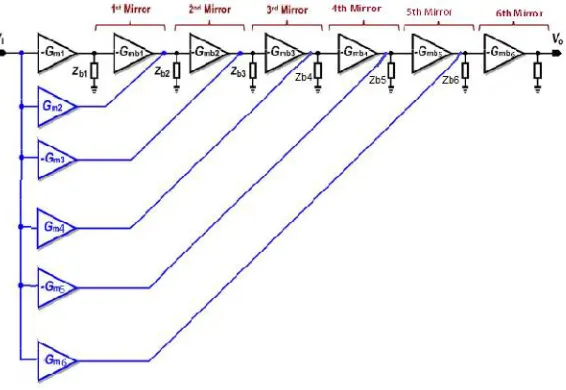
Figure 5: Block diagram of the proposed 6-step NCM amplifier
Mirror factors (K) selected for the circuit design case can be mention as K1 = 7, K2 = 6, K3 = 7, K4 = 12, K5 = 15, K6 =
1:5, K7 = 38, K8 = 10, K9 = 27, K10 = 11, K11 = 16. For the 6-step NCM, the total bias current (3 µA) is divided into 240
unit-current (Iu = 12.5nA ). To leverage the key metrics, the 1st mirror (M7 - M8 ) uses a small ratio of only 1 (K1 = 7
and K2 = 6 ). The 2nd mirror (M9 - M10 ) draws less current under a ratio of 1 (K3 = 7 and K4 = 12) to boost the DC gain
and GBW, as they contribute less noise. Also, a larger K7 enhances the SR. The last mirror (M17 - M18 ) is assigned the
largest ratio (K11 = 16 ) to benefit the SR and GM, NCM6. Substituting these values into the DC gain, GBW and SR
equation we can see that these are theoretically improved.
The equivalent small-signal diagram of the 6-step NCM amplifier is shown in Figure 5. Gm1, Gm2, Gm3, Gm4,
Gm5 and Gm6 are the transconductancesof M1-6 respectively while Zb1, Zb2, Zb3, Zb4, Zb5 and Zb6 correspond to the input
impedances of the 1st to 6th mirrors. The transconductances of the transistors in the six mirrors are respectively represented by Gmb1-6, while Zout models the output impedance that includes CL.
VII. EXPERIMENTAL RESULTS OF 5-STEP AND 6-STEP NCM
Figure 6: AC response of 5-step NCM
Figure 7: AC response of 6-step NCM
Slew rate determines the amplifiers settling performance. Slew rate can also defined as the rate of change of output or how quickly the output change with respect to the given input. When a large negative step appears at VP, the value of
negative SR obtained at the output. Similarly a large positive at VP leads to positive SR. Therefore we give a dc pulse
current at the VP, which results a symmetric SR. If the load capacitance change from 250 pF to 1 nF the slew response
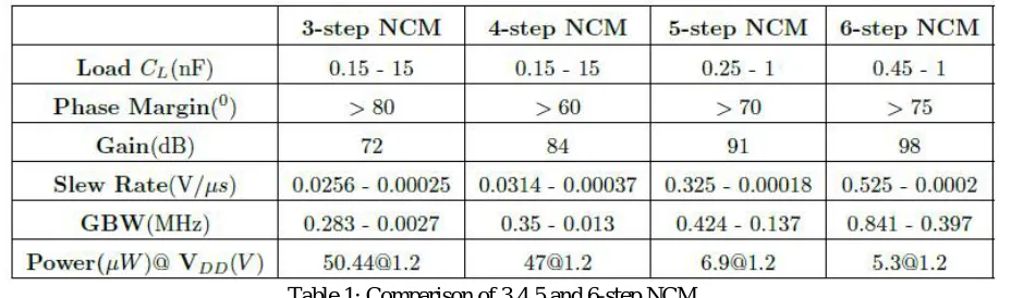
Table 1: Comparison of 3,4,5 and 6-step NCM
Table 1 represent comparison of different topologies. From the table we can conclude that as the step size increases the performance of the single stage amplifiers improved from the previous stages.
VI. CONCLUSION
This paper introduced a NCM single-stage amplifier that has more design flexibilities with mirror steps and sub mirror ratios to optimize the performance metrics (GBW, DC gain and SR), while preserving a rail-to-rail output swing, and wide CL drivability without entailing any compensation capacitor or resistor. Both the performance limits and robustness of the NCM technique have been analytically explored. Two prototypes, 5-step and 6-step NCM amplifiers, were designed and analyzed in 180 nm CMOS technology for systematic comparison with 3-step and 4-step NCM.
REFERENCES
[1] Zushu Yan, Pui-In Mak, Rui P. Martins and Franco Maloberti, “Nested-Current-Mirror Rail-to-Rail-Output Single-Stage Amplifier With Enhancements of DC Gain, GBW and Slew Rate, ”IEEE journal of solid-state circuits, vol. 50, no. 10, october 2015
[2] Y.-S. Son et al., “A column driver with low-power area-efficient pushpullbuffer amplifiers for active-matrix LCDs,” in IEEE ISSCC Dig. Tech. Papers, 2007, pp. 142–143.
[3] C.-W. Lu, P.-Y.Yin, C.-M.Hsiao, M.-C.Chang, and Y.-S. Lin, “A 10-bit resistor-floating-resistor-string DAC (RFR-DAC) for high color-depth LCD driver ICs,” IEEE J. Solid-State Circuits, vol. 47, no. 10, pp. 2454–2466, Oct. 2012..
[4] K. N. Leung and P. K. T. Mok, “Analysis of multistage amplifier-frequency compensation,” IEEE Trans. Circuits Syst. I, vol. 48, no. 9, pp. 1041–1056, Sep. 2001.
[5] Z. Yan, P.-I.Mak, M.-K. Law, R. P. Martins, and F. Maloberti, “A 0.013 mm 3.6 W nested-current- mirror single-stage amplifier driving 0.15-to-15 nF capacitive load with 62 phase margin,” in IEEE ISSCC Dig. Tech. Papers, 2014, pp. 288–289..
[6] M. Ho, K. N. Leung, and K. Mak, “A low-power fast-transient 90-nm low-dropout regulator with multiple small-gain stages,” IEEE J. Solid-State Circuits, vol. 45, no. 11, pp. 2466–2475, Nov. 2010.
[7] K. H. Mak and K. N. Leung, “A signal- and transient-current boosting amplifier for large capacitive load applications,” IEEE Trans. Circuits Syst. I, vol. 61, no. 10, pp. 2777–2785, Oct. 2014.
[8] L. Yao, M. Steyaert, and W. Sansen, “A 1-V 140- W 88 dB audio sigma-delta modulator in 90-nm CMOS,” IEEE J. Solid-State Circuits, vol. 39, no. 11, pp. 1809–1818, Nov. 2004.
[9] J. Roh, “High-gain class-AB OTA with low quiescent current,” J. Analog Integr. Circuits Signal Process., vol. 47, no. 2, pp. 225–228, May 2006. [10] J. Roh, S. Byun, Y. Choi, H. Roh, Y.-G.Kim, and J.-K. Kwon, “A 0.9-V 60- W 1-bit fourth-order delta-sigma modulator with 83 dB dynamic range,” IEEE J. Solid-State Circuits, vol. 43, no. 2, pp. 361–370, Feb. 2008.