Analysis of Low Power, Area- Efficient and High Speed
Multiplier using Fast Adder
Krishna Naik Dungavath1, Dr V.Vijayalakshmi2
1
Ph.D. Scholar , Dept. of ECE, Pondecherry Engineering College, Puducherry
2 Asst.Professor, Dept. of ECE, Pondecherry Engineering College, Puducherry
Email: [email protected], [email protected]
ABSTRACT
In this paper the performance of different types of adders are analysed. And carry select adder (CSLA) is the lowest delay compare to other adders. Carry select adder is one of the fastest adders used in many data-processing processors to perform fast arithmetic functions. From the structure of the CSLA, there is a possibility for increasing the speed and reducing the area and in the CSLA. This work uses a simple and efficient gate- level modification to significantly reduce the area and power of the CSLA. Based on this modification 16 bit CSLA architecture have been developed and compared with the regular CSLA architecture. The proposed design has increased speed and reduced area and power as compared with the regular CSLA with only a slight increase in the delay. This work evaluates the performance of the proposed designs in terms of delay, speed (frequency) and memory. The results analysis shows that the proposed CSLA structure is better than the regular CSLA. And it is implemented in multiplier as application for efficient performance.
Keywords- carry select adder(CSLA), carry save adder ,carry skip adder, RCA, BEC,AOI.
I. INTRODUCTION
Design of area- and power-efficient high-speed data path logic systems are one of the most substantial areas of research to perform arithmetic operations in VLSI design there is a scope for reducing area and delay. There is a scope of CSLA in VLSI system design. In digital adders, the speed of addition is limited by the time required to propagate a carry through the adder. The sum for each bit position in an elementary adder is generated sequentially only after the previous bit position has been summed and a carry propagated into the next position. The circuit architecture is simple and area-efficient. However, the computation speed is slow because each full-adder can only start operation till the previous carry-out signal is ready.
On the other hand, Carry Look-ahead Adders (CSLAs) are the fastest adders, but they are the worst
from the area point of view. Carry Select Adders have been considered as a compromise solution between RCAs and CSLAs because they offer a good tradeoff between the compact area of RCAs and the short delay of CSLAs. Reduced area and high speed data path logic systems are the main areas of research in VLSI system design. High speed addition and multiplication has always been a fundamental requirement of high-performance processors and systems. The sum for each bit position in an elementary adder is generated sequentially only after the previous bit position has been summed and a carry propagated into the next position. There are many types of adder designs available (Ripple Carry Adder, Carry Look Ahead Adder, Carry Save Adder, Carry Skip Adder) which have its own advantages and disadvantages. The major speed limitation in any adder is in the production of carries and many authors considered the addition problem. To solve the carry propagation delay CSLA is developed which drastically reduces the area and delay to a great extent.
The CSLA is used in many computational systems design to moderate the problem of carry propagation delay by independently generating multiple carries and then select a carry to generate the sum. It uses independent ripple carry adders (for Cin=0 and Cin=1) to generate the resultant sum. However, the Regular CSLA is not area and speed efficient because it uses multiple pairs of Ripple Carry Adders (RCA) to generate partial sum and carry by considering carry input. The final sum and carry are selected by the multiplexers (mux). Due to the use of two independent RCA the area will increase which leads an increase in delay. To overcome the above problem, the basic idea of the proposed work is to use n-bit binary to excess-1 code converters (BEC) to improve the speed of addition. This logic can be replaced in RCA for Cin=1 to further improves the speed and thus reduces the delay.
main advantage of this BEC logic comes from the lesser number of logic gates than the Full Adder (FA) structure because the number of gates used will be decreased. This work in brief is structured as follows. Section II deals with the delay and area evaluation methodology of the basic adder blocks and its corresponding delay and area values
The main advantage of this BEC logic comes from the lesser number of logic gates than the n-bit Full Adder (FA) structure. Rest of the paper is organized as follows section II provides the basic idea of sequence adder. Section III provides analysis of the various adders. section IV provides the proposed design structure. Section V Overview of Multiplication VI provides the simulated results that analysis of delay, frequency and memory of adders and section VII conclude the work.
II. ARCHITECTURE OF RIPPLE CARRY ADDER
An n-bit Ripple Carry Adder (RCA) is a simple cascading of n full adders as shown in Figure 2. In the RCA, the carry bit ripples from one stage of the adder chain to the next.
Fig 1: Ripple carry adder architecture
The worst-case delay of the RCA is when a carry signal transition ripples through all stages of adder chain from the least significant bit to the most significant bit, which is approximated by:
where tc is the delay through the carry stage of a full adder, and ts is the delay to compute the sum of the last stage. The delay of ripple carry adder is linearly proportional to n, the number of bits, therefore the performance of the RCA is limited when n grows bigger. The advantages of the RCA are lower power consumption as well as a compact layout giving smaller chip area.Concatenating the N full adders forms N bit Ripple carry adder. In this carry out of previous full adder becomes the input carry for the next full adder. It calculates sum and carry according to the following equations. As carry ripples from one
full adder to the other, it traverses longest critical path and exhibits worst-case delay.
RCA is the slowest in all adders (O (n) time) but it is very compact in size (O (n) area). If the ripple carry adder is implemented by concatenating N full adders, the delay of such an adder is 2N gate delays from Cin to Cout. The delay of adder increases linearly with increase in number of bits.
III. ANALYSIS OF ADDERS A. Carry Skip Adder
A carry skip divides the words to be added in to groups of equal size of k-bits. Carry Propagate pi signals may be used within a group of bits to accelerate the carry propagation. If all the pi signals within the group are pi=1, carry bypasses the entire group . P = pi * pi+1 * pi+2 *… pi+k In this way delay is reduced as compared to ripple carry adder. The idea behind Variable Block Adder (VBA) is to minimize the critical path delay in the carry chain of a carry skip adder, while allowing the groups to take different sizes. In case of carry skip adder, such condition will result in more number of skips between stages. Such adder design is called variable block design, which is tremendously used to fasten the speed of adder. In the variable block carry skip adder design we divided a 32-bit adder in to 4 blocks or groups. The bit widths of groups are taken as; First block is of 4 bits, second is of 6 bits, third is 18 bit wide and the last group consist of most significant 4 bits. That the logic utilization of carry skip and variable carry skip 32-bit adder. The power and delay, which are obtained also given in the table. From table it can be observed that variable block design consumes more area as gate count and number of LUT’s consumed by variable block design is more than conventional carry skip adder are composed of ripple carry adder blocks of fixed size* and a carry skip chain .The size of the blocks are chosen so as to minimize the longest life of a carry Boolean Equations Carry Propagate: Pi= Ai^Bi Sum: Si= Pi^Ci Carry Out: Ci+1= Ai Bi+ Pi Ci
B. Carry Save Adder
Fig.2:Block Diagram of Carry Save Adder
of adding together m numbers (all n bits wide) is to add the first two, then add that sum to the next, and
so on. This requires a total of m − 1 additions, for a total gate delay of the order of mlog n or O(mlog n), assuming look-ahead carry adders
The important point is that c and s can be computed independently, and furthermore, each ci (and si) can be computed independently from all of the other c’s (and s’s). This achieves our original goal of converting three numbers that we wish to add into two numbers that add up to the same sum, and in O(1) time. A carry-save adder is a type of digital adder it is used in computer micro architecture to compute the sum of three or more n-bit numbers in binary. It differs from other digital adders in that it outputs two numbers of the same dimensions as the inputs. one which is a sequence of partial sum bits and another which is a sequence of carry bits.
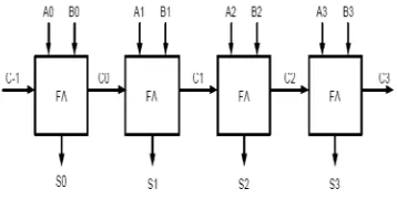
C. Carry Select Adder
Fig.3:Block Diagram of Regular 16b Carry Select Adder
The carry select adder comes in the category of conditional sum adder. Conditional sum adder works on some condition. Sum and carry are calculated by assuming input carry as 1 and 0 prior the input carry comes. When actual carry input arrives, the actual calculated values of sum and carry are selected using a multiplexer. The conventional carry select adder consists of k/2 bit adder for the lower half of the bits i.e. least significant bits and for the upper half i.e. most significant bits (MSB’s) two k/ bit adders. In MSB adders one adder assumes carry input as one for performing addition and another assumes carry input as zero. The carry out calculated from the last stage i.e. least significant bit stage is used to select the actual calculated values of output carry and sum. The selection is done by using a multiplexer. This technique of dividing adder in to stages increases the area utilization but addition operation fastens. It is composed of two four-bit ripple carry adders per section. Both sum and carry bits are calculated for the
two alternatives of the input carry, ―0‖ and ―1‖.The
carry out of each section determines the carry in of the next section, which then selects the appropriate ripple carry adder. The very first section has a carry in of zero. Time delay: time to compute first section + time to select sum from subsequent sections.
IV. MODIFIED CARRY SELECT ADDER USING BEC
As stated above the main idea of this work is to use BEC instead of the RCA with Cin=1 in order to reduce the area and power consumption of the regular CSLA. To replace the n-bit RCA, an n+1-bit BEC is required. A structure and a 4-b BEC are shown in Fig.4.
Fig.4:4-b BEC
The Boolean expressions of the 4-bit BEC is listed as (note the functional symbols ~ NOT, & AND,^XOR) X0=~B0
X1=B0^B1 X2=B2^(B0&B1) X3=B3^(B0&B1&B2)
Fig.5:Block Diagram of modified 16b Carry Select Adder
Fig.6:Block Diagram of proposed 16b Carry Select Adder
The structure of the proposed 16-b SQRT CSLA using BEC for RCA with Cin = 1 to optimize the area and power is shown in Fig. 5. We again split the structure into five groups. The delay and area estimation of each group. The steps leading to the evaluation are given here
The group2 has one 2-b RCA which has 1 FA and 1 HA for Cin = 0. Instead of another 2-b RCA with Cin = 1 a 3-b BEC is used which adds one to the output from 2-b RCA. Based on the consideration of delay values of Table I, the arrival time of selection input C1 [time(t) = 7] of 6:3 mux is earlier than the S3 [t=9] and C3 [t=10] and later than the S2 [t=4]. Thus, the sum3 and final C3 (output from mux) are depending on S3 and mux and partial C3 (input to mux) and mux, respectively. The sum2 depends on C1 and mux. For the remaining group’s the arrival time of mux selection input is always greater than the arrival time of data inputs from the BEC’s. Thus, the delay of the remaining groups depends on the arrival time of mux selection input and the mux delay. V. OVERVIEW OF MULTIPLICATION A. Unsigned Multiplication
The hardware architecture of 2X2, 4x4 and 8x8 bit Vedic multiplier module are displayed in the below sections. Here, “Urdhva-Tiryagbhyam” (Vertically and Crosswise) sutra is used to propose such architecture for the multiplication of two binary numbers. The beauty of Vedic multiplier is that partial product generation and additions are done concurrently. Hence, it is well adapted to parallel processing. The feature makes it more attractive for binary multiplications. This in turn reduces delay, which is the primary motivation behind this work. A. Vedic Multiplier for 2x2 bit Module
The method is explained below for two, 2 bit numbers A and B where A = a1a0 and B = b1b0 as shown in Fig. 7. Firstly, the least significant bits are multiplied which gives the least significant bit of the final product (vertical). Then, the LSB of the multiplicand is multiplied with the next higher bit of the multiplier and added with, the product of LSB of multiplier and next higher bit of the multiplicand (crosswise). The sum gives second bit of the final
product and the carry is added with the partial product obtained by multiplying the most significant bits to give the sum and carry. The sum is the third corresponding bit and carry becomes the fourth bit of the final product
s0 = a0b0; (1) c1s1 = a1b0 + a0b1; (2) c2s2 = c1 + a1b1; (3)
The final result will be c2s2s1s0. This multiplication method is applicable for all the cases.
Fig.7 The Vedic Multiplication Method For Two 2 Bit Binary Numbers
The 2X2 Vedic multiplier module is implemented using four input AND gates & two half-adders which is displayed in its block diagram in Fig. 8. It is found that the hardware architecture of 2x2 bit Vedic multiplier is same as the hardware architecture of 2x2 bit conventional Array Multiplier .Hence it is concluded that multiplication of 2 bit binary numbers by Vedic method does not made significant effect in improvement of the multiplier’s efficiency.
Very precisely we can state that the total delay is only 2-half adder delays, after final bit products are generated, which is very similar to Array multiplier. So we switch over to the implementation of 4x4 bit Vedic multiplier which uses the 2x2 bit multiplier as a basic building block. The same method can be extended for input bits 4 & 8. But for higher no. of bits in input, little modification is required.
Fig.8. Block Diagram Of 2x2 Bit Vedic Multiplier B. Vedic Multiplier for 4x4 bit Module
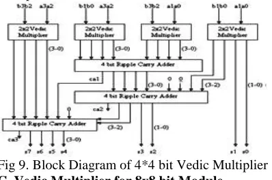
block, we can have the following structure for multiplication as shown in Fig. 8. Fig. 9 Sample Presentation For 4x4 Bit Vedic Multiplication Each block as shown above is 2x2 bit Vedic multiplier. First 2x2 bit multiplier inputs are A1A0 and B1B0. The last block is 2x2 bit multiplier with inputs A3 A2 and B3 B2. The middle one shows two 2x2 bit multiplier with inputs A3 A2 & B1B0 and A1A0 & B3 B2. So the final result of multiplication, which is of 8 bit, S7S6S5S4 S3 S2 S1 S0. To understand the concept, the Block diagram of 4x4 bit Vedic multiplier is shown in Fig. 9. To get final product (S7 S6 S5 S4 S3 S2 S1 S0), four 2x2 bit Vedic multiplier and three 4-bit Ripple-Carry (RC) Adders are required. The proposed Vedic multiplier can be used to reduce delay. Early literature speaks about Vedic multipliers based on array multiplier structures. On the other hand, we proposed a new architecture, which is efficient in terms of speed. The arrangements of ripple carry Adders shown in Fig. 3, helps us to reduce delay and 8x8 Vedic multiplier modules are implemented easily by using four 4x4 multiplier modules.
Fig 9. Block Diagram of 4*4 bit Vedic Multiplier C. Vedic Multiplier for 8x8 bit Module
The 8x8 bit Vedic multiplier module as shown in the block diagram in Fig. 10 can be easily implemented by using four 4x4 bit Vedic multiplier modules as discussed in the previous section. Let’s analyze 8x8 multiplications, say A= A7 A6 A5 A4A3 A2 A1 A0 and B= B7 B6 B5B4 B3 B2 B1B0. The output line for the multiplication result will be of 16 bits as – S15 S14 S13S12 S11 S10 S9 S8 S7 S6S5S4 S3 S2 S1 S0. Let’s divide A and B into two parts, say the 8 bit multiplicand A can be decomposed into pair of 4 bits AH-AL. Similarly multiplicand B can be decomposed into BH-BL. The 16 bit product can be written as:P = A x B = (AH-AL) x (BH-BL) = AH x BH + (AH x BL + AL x BH) + AL x BL Using the fundamental of Vedic multiplication, taking four bits at a time and using 4 bit multiplier block as discussed we can perform the multiplication. The outputs of 4x4 bit multipliers are added accordingly to obtain the final product. Here total three 8 bit Ripple-Carry Adders are required as shown in Fig. 10.
Fig. 10 Block Diagram Of 8x8 Bit Vedic Multiplier d.Vedic Multiplier for 16x16 bit Module
The design of 16×16 block is a similar arrangement of 8×8 blocks in an optimized manner .The first step in the design of 16×16 block will be grouping the 8 bit (byte) of each 16 bit input. These lower and upper bytes pairs of two inputs will form vertical and crosswise product terms. Each input byte is handled by a separate 8×8 Vedic multiplier to produce sixteen partial product rows. These partial products rows are added in a 16-bit carry look ahead adder optimally to generate final product bits. The schematic of a 16×16 block designed using 8×8 blocks. The partial products represent the Urdhva vertical and cross product terms. Then using or and half adder assembly to find the final product. Power dissipation of this multiplier is 0.18 mW and propagation delay is 6.216 nsec.
Fig 11 Block Diagram Of 16 X 16 Bit Vedic Multiplier
VI. Implementation In Xilinx13.2
In this work,16x16 bit Vedic multiplier is designed in verilog (Very High Speed Integrated Circuits Hardware Description Language). Logic synthesis and simulation was done in XilinxISE13.2i - Project Navigator and ISim simulator integrated in the Xilinx package. The performance of circuit is evaluated on the Xilinx device family Spartan3, package vq100 and speed grade -4.TheRTL schematic of 16x16 bit Vedic multiplier.
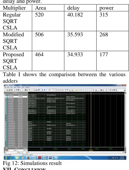
parameters on which they are compared are area, delay and power.
Multiplier Area delay power Regular
SQRT CSLA
520 40.182 315
Modified SQRT CSLA
506 35.593 268
Proposed SQRT CSLA
464 34.933 177
Table I shows the comparison between the various adders
Fig 12: Simulations result VII. CONCLUSION
Power, delay and area are the constituent factors in VLSI design that limits the performance of any circuit. This work presents a simple approach to reduce the area, delay and power of CSLA architecture. The conventional carry select adder has the disadvantage of more power consumption and occupying more chip area. The proposed SQRT CSLA using And-Or-Inverter logic has low power, less delay and reduced area than all the other adder structures. It is also little bit faster than all the other adders. In this way, the transistor count of proposed SQRT CSLA is reduced having less area and low power which makes it simple and efficient for VLSI hardware implementations. . The results analysis shows that the proposed CSLA structure is better than the regular CSLA. And it is implemented in multiplier as application for efficient performance
REFERENCES
[1] O. J. Bedrij, ―Carry-select adder,‖ IRE Trans. Electron. Comput., pp.340–344, 1962.
[2] B. Ramkumar, H.M. Kittur, and P. M. Kannan,
―ASIC implementation of modified faster carry save
adder,‖ Eur. J. Sci. Res., vol. 42, no. 1, pp. 53–58, 2010
[3] T. Y. Ceiang and M. J. Hsiao, ―Carry-select
adder using single ripple carry adder,‖ Electron. Lett.,
vol. 34, no. 22, pp. 2101–2103, Oct. 1998.
[4] Y. Kim and L.-S. Kim, ―64-bit carry-select
adder with reduced area,‖Electron. Lett., vol. 37, no.
10, pp. 614–615, May 2001.
[5] J. M. Rabaey, Digtal Integrated Circuits—A Design Perspective. Upper Saddle River, NJ: Prentice-Hall, 2001
[6] Y. He, C. H. Chang, and J. Gu, ―An area
efficient 64-bit square root carry-select adder for
lowpower applications,‖ in Proc. IEEE Int.
Symp.Circuits Syst., 2005, vol. 4, pp. 4082–4085.
[7] K. Rawwat, T. Darwish, and M. Bayoumi, ―.A low power carry select adder with reduces area‖,
Proc. Of Midwest Symposium on Circuits and Systems, pp. 218- 221, 2001.
[8] A. Tyagi, ―A reduced area scheme for carry
-select adders‖,IEEE Trans. on Computer, vol. 42, pp.
1163- 1170, 1993
[9] Y. Kim and L-S Kim, ―64-bit carry-select adder
with reduced area‖, Electronics Letters, vol. 37, pp. 614-615, May 2001.
[10] Hasan Krad and Aws Yousif Al-Taie,
―Performance Analysis of a 32-Bit Multiplier with a Carry-Look-Ahead Adder and a 32-bit Multiplier
with a Ripple Adder using VHDL‖, Journal of
Computer Science 4 (4): 305-308, 2008.
AUTHORS:
First Author- Mr Krishna Naik Dungavath received the BTech Degree from SV University Tirupati, and M.E From University College of Enginnering(A), Osmania University, Hyderabad, He Pursing Ph.D in Pondechery Engineering College Puducherry. Currently working as Asst.Professor in the Department of Electronics and Communication Engineering, in PVVK institute of Technology, Anantapur. Areas of interests are ,VLSI, ASIC,Wireless Communication and Digital Systems Email address: [email protected]
Second Author – Dr. V.Vijayalakshmi, M.Tech,.Ph.D, ASST.Professor in the Department of Electronics and Communication Engineering, in Pondechery engineering College, Puducherry Areas of interests are Cryptography, Information and Network Security,VLSI,ASIC
Email address: [email protected] Correspondence Author :