International Journal of Research (IJR)
e-ISSN: 2348-6848, p- ISSN: 2348-795X Volume 2, Issue 07, July 2015Available at http://internationaljournalofresearch.org
Design and Implementation an Efficient Hardware Utilization for
Testing Applications by UART with BIST
1
T.Sreenath,
PG Student ,
Sri Krishnadevaraya Engg College,NH44,GOOTY,ANANTAPURAM (DIST),
ANDHRA PRADESH,,PIN-515401
2
S.T.Mrudula
M.Tech., Sri Krishnadevaraya Engg College,NH44,GOOTY,ANANTAPURAM (DIST),
ANDHRA PRADESH,,PIN-515401
Abstract:
BIST is a design-for-testability technique that places the testing functions physically with
the circuit under test (CUT). The basic BIST architecture requires the addition of three blocks to
a digital circuit which are a test pattern generator, a response analyzer, and a test controller.
The test pattern generator generates the test patterns for the CUT. An LFSR is used as a pattern
generator to generate the patterns. A typical response analyzer is a comparator with stored
responses. It analyzes the test responses to determine correctness of the CUT. A test control
block is necessary to activate the test and analyze the responses. However, in general, several
test-related functions can be executed through a test controller circuit.In this project, the design
is implemented by using of a LFSR. In the initial state, the LFSR output will be set to 0. Later, on
occurrence of each clock, the value will be incremented by 1, but when the output reaches to the
value of 511, again the LFSR resets to 0. Thus the 9-bit LFSR is capable to generate all possible
Test patterns. The patterns generated by the LFSR are applied to the UART (CUT).In the UART
it is required to perform an addition operation at one instance. So, we implemented the addition
operation by using Reversible Logic Gates. By using this technique, power consumption is
reduced compared with normal adders. This project is implemented by VERILOG HDL in Xilinx
12.3i with the device XC3S500E-5fg320.
Keyword: LFSR; Optimization; Test Pattern generation; UART
1.
INTRODUCTION
The main challenging areas in VLSI
are performance, cost, power dissipation is
due to switching i.e. the power consumed
testing, due to short circuit current flow and
charging of load area, reliability and power.
The demand for portable computing devices
and communications system are increasing
rapidly. The applications require low power
dissipation VLSI circuits. The power
International Journal of Research (IJR)
e-ISSN: 2348-6848, p- ISSN: 2348-795X Volume 2, Issue 07, July 2015Available at http://internationaljournalofresearch.org
factor in the power dissipation is the dynamic
power which is consumed when the circuit
nodes switch from 0 to 1. During switching,
the power is consumed due to the short circuit
current flow and the charging of load
capacitances is given by equation:
P = 0.5VDD2E (sw) CLFCLK (1)
Where VDD is supply voltage, E(sw) is the
average number of output transitions per 1/
FCLK, FCLK is the clock frequency and CL
is the physical capacitance at the output of the
gate. Dynamic power dissipation contributed
to total power dissipation. From the equation
dynamic power depends on three parameters:
supply voltage, clock frequency and switching
activity. To reduce the dynamic
power dissipation by using first two parameters only at the expense of circuit performance. But power reduction using the switching activity doesn't degrade the performance of the circuit. Power dissipation during testing is one of most important issue. Latest advances in semiconductor technology have led to transistor scaling of transistor dimensions, allowing a large number of devices to be fabricated on a single chip. The high integration has made power consumption. In addition, the ever increasing utilization of portable computing devices and communication systems requires low power dissipation in VLSI circuits. The power dissipation of a system in test mode is more than in normal mode. Low correlation between consecutive test vectors (e.g. among pseudorandom patterns) increases switching activity and eventually power dissipation in the circuit. The same happens when applying low correlated patterns to scan chains. Increasing switching activity in scan chain results in increasing power consumption in scan chain and combinational block. The extra power (average or peak) can cause problems such as instantaneous power surge causes circuit damage, formation of hot spots, difficulty in performance verification
International Journal of Research (IJR)
e-ISSN: 2348-6848, p- ISSN: 2348-795X Volume 2, Issue 07, July 2015Available at http://internationaljournalofresearch.org
combinational circuits while attaining high fault coverage. Test time and area overhead remain unaffected. Another low-power test pattern generator based on a modified LFSR is proposed in. The scheme reduces the power in CUT in general and clock tree in particular. Gizopoulos et al. consider the problem of low-power BIST for data path architecture built around multiplier-accumulator pairs. The method proposes two alternative architectures depend on low energy or low power dissipation. The authors based on both modified binary counters, operating as Gray counters, generate only one transition at a time. These architectures can achieve important energy and average power savings compared to conventional pseudorandom BIST. The drawback of these techniques is circuit-dependent, implying that non-detecting subsequences must be determined for each circuit test sequence. Other authors propose two other low-power approaches for scan-based BIST. Zhang, Roy, and Bhawmik propose modifying the LFSR by adding weight sets to tune the pseudorandom vector‟s signal probabilities and thereby decrease energy consumption and increase fault coverage.A low-power random pattern generation technique to reduce signal activities in the scan chain is proposed in. In this technique, an LFSR generates equally probable random patterns. The technique generates random but highly correlated neighboring bits in the scan chain, reducing the number of transitions and, thus, the average power. Girard etal. address the problem of energy minimization during test application for BIST enabled circuits. The main constraint is reducing energy consumption without modifying the stuck-at fault coverage. In this work, the authors first analyze the impact of an LFSR‟s polynomial and seed selection on the circuit‟s switching activity during test application. They determine that the polynomial selection does not influence energy consumption; the LFSR‟s seed selection is a more important parameter. Therefore, the authors
propose a method based on a simulated- annealing algorithm to select
2.
UART DESCRIPTION
This chapter mainly explains the Overview of serial communication and UART description, functions, character transmitter, character receiver, features and uses.
2.1 An Overview Of Serial
Communication
Serial communication is the process of sending data and receiving one bit of data at one time sequentially through a communications channel or computer bus. On the other hand, parallel communications is a process where all the bits of each symbol are sent together. In general, serial communication is used for all long communications and most computer networks where it is impractical to use parallel communications due to the cost of cable and synchronization. Nowadays computer buses or network communication using serial communications are becoming more common as improved technology enables them to transfer data at higher speeds.
There are 2 types of serial communication, full duplex and half duplex. A full duplex device can send and receive data at the same time. Thus, a full duplex communication needs 2 different ports, one for serial in data while another for serial out data. On the other hand, half duplex serial devices support only one-way communications and therefore only able either receiving or transmitting data at a time. Normally half duplex devices share the same port for both serial in and out.
2.1.1Overview of UART
International Journal of Research (IJR)
e-ISSN: 2348-6848, p- ISSN: 2348-795X Volume 2, Issue 07, July 2015Available at http://internationaljournalofresearch.org
hardware that commonly used in PC serial port to translate data between parallel and serial interfaces. The UART takes bytes of data and transmits the individual bits in a sequential fashion. At the receiving point, UART re-assembles the bits into complete bytes.
Asynchronous transmission allows
data to be transmitted without having to send a
clock signal to the receiver. Thus, the sender
and receiver must agree on timing parameters
in advance and special bits are added to each
word, which is used to synchronize the
sending and receiving units. In general,
UART contains of two main block, the
transmitter and receiver block. The
transmitter sends a byte of data bit by bit
serially out from UART while UART receiver
receives the serial in data bit by bit and
converts them into a byte of data.
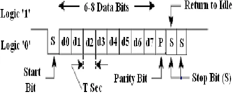
UART starts the data transmission by
asserting a bit called the "Start Bit" to the
beginning of each data that is to be
transmitted. The Start Bit is also used to
inform the receiver that a byte of data is about
to be sent. After the Start Bit, the individual
bits of the “byte” of data are sent, with the
Least Significant Bit (LSB) being sent first.
Each bit in the transmission is transmitted for
exactly the same amount of time as all of the
other bits. On the other, UART the receiver
will need to sample the logic value that being
received at approximately halfway through the
period assigned to each bit to determine if it is
logic 1 or logic 0.
When a byte of data has been sent, the
transmitter may add a “Parity Bit”. The
receiver to perform simple error checking may
use the Parity Bit. In this project, parity bit is
not being implemented. After this, a “Stop
Bit” is sent by the transmitter to indicate the
transmitter
has
completed
the
data
transmission. If another byte of data is to be
transmitted, the Start Bit for the new data can
be sent as soon as the Stop Bit for the previous
word has been sent.
Fig. 2.1 UART data frame format
The speed of the serial connection is measured in bits-per-second or normally expressed as "baud rate". The duration of a bit is dependent on the baud rate. The baud rate is the number of times the signal can switch states in one second. Thus, if the line is operating at 9600 baud, the line can switch states 9,600 times per second. This means each bit has the duration of 1/9600 of a second or about 100 micro second.
Serial data is transmitted via its serial
port. A serial port is one of the most
universal parts of a computer. It is a
connector where serial line is attached and
connected to peripheral devices such as
mouse, modem, printer and even to another
computer.
In
contrast
to
parallel
communication, these peripheral devices
communicate using a serial bit stream protocol
(where data is sent one bit at a time). The
serial port is usually connected to UART, an
integrated circuit that handles the conversion
between serial and parallel data.
International Journal of Research (IJR)
e-ISSN: 2348-6848, p- ISSN: 2348-795X Volume 2, Issue 07, July 2015Available at http://internationaljournalofresearch.org
tones or sounds (the audio tones are sinusoidal shaped signals). This conversion is performed by a peripheral device called a modem (modulator/demodulator). The modem takes the signal on the single wire and converts it to sounds. At the other end, the modem converts the sound back to voltages, and another UART converts the stream of 0’s and 1’s back to bytes of parallel data.
Fig. 2.2 Serial Data Transmission And
Receive
UART functions
• Transmitter– Convert from parallel to serial – Add start and stop delineators (bits) – Add parity bit
• Receiver
– Convert from serial to parallel
– Remove start and stop delineators (bits)
– Check and remove parity bit
3.BIST ARCHITECTURE:
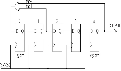
A typical BIST architecture consists of TPG - Test Pattern Generator,TRA – Test Response Analyzer,Control Unit As shown in figure below.
Fig 3.1 Test Pattern Generator
It generates test pattern for CUT. It will be dedicated circuit or a micro processor. Pattern generated may be pseudo random numbers or deterministic sequence. Here we are using a
Linear Feedback Shift Register for generating random number. The Architecture for LFSR is as shown below.
Fig 3.2 The Architecture for LFSR
Tapping can be taken as we wish but as per taping change the LFSR output generate will change & as we change in no of flip-flop the probability of repetition of random number will reduce. The initial value loading to the LFSR is known as seed value.
Test Response Analyzer (TRA):
TRA will check the output of MISR & verify with the input of LFSR & give the result as error or not.
BIST Control Unit:
Control unit is used to control all the operations. Mainly control unit will do configuration of CUT in test mode/Normal mode, feed seed value to LFSR, Control MISR & TRA. It will generate interrupt if an error occurs. You can clear interrupt by interrupt_clear_i signal.
Circuit under Test (CUT):
CUT is the circuit or chip in which we are going to apply BIST for testing stuck at zero or stuck at one error.
Need for using BIST technique
International Journal of Research (IJR)
e-ISSN: 2348-6848, p- ISSN: 2348-795X Volume 2, Issue 07, July 2015Available at http://internationaljournalofresearch.org
boards with fine-pitch ICs are virtually
impossible to be accessed physically for
testing. Traditional board test methods which
include functional test, only accesses the
board's primary I/Os, providing limited
coverage and poor diagnostics for
board-network fault. In circuit testing, another
traditional test method works by physically
accessing each wire on the board via costly
"bed of nails" probes and testers. To identify
reliable testing methods which will reduce
the cost of test equipment, a research to
verify each VLSI testing problems has
been conducted. The major problems detected
so far are as follows:
Test generation problems
Gate to I/O pin ratio
• Test Generation Problems
The large number of gates in VLSI
circuits has pushed computer
automatic-test-generation times to weeks or months of
computation. The numbers of test patterns
are becoming too large to be handled by
an external tester and this has resulted in
high computation costs and has outstripped
reasonable available time for production
testing.
• The Gate to I/O Pin Ratio Problem
As ICs grow in gate counts, it is no longer true that most gate nodes are directly accessible by one of the pins on the package. This makes testing of internal nodes more difficult as they could neither no longer be easily controlled by signal from an input pin (controllability) nor easily observed at an output pin (observe ability). Pin counts go at a much slower rate than gate counts, which worsens the controllability and observe ability of internal gate nodes.Serial-in, parallel-out (SIPO):
This configuration allows conversion from
serial to parallel format. Data is input serially.
Once the data has been input, it may read off
at each output simultaneously.
4-Bit SIPO
SIPO registers are commonly attached to the output of microprocessors when more output pins are required than are available. This allows several binary devices to be controlled using only two or three pins - the devices in question are attached to the parallel outputs, then the desired state of all those devices can be sent out of the microprocessor using a single serial connection. Similarly, PISO configurations are commonly used to add more binary inputs to a microprocessor than are available - each binary input (i.e. a switch or button, or more complicated circuitry designed to output high when active) is attached to a parallel input .
International Journal of Research (IJR)
e-ISSN: 2348-6848, p- ISSN: 2348-795X Volume 2, Issue 07, July 2015Available at http://internationaljournalofresearch.org
pausing the display output to skip one line of characters.
Serial-in, parallel-out shift register
A serial-in/parallel-out circut is that it shifts
data into internal storage elements and shifts
data out in the parallel fashion. Therefore, a
serial-in/parallel-out shift register converts
data from serial format to parallel format. If
four data bits are shifted in by four clock
pulses via a single wire at data-in, the data
becomes available simultaneously on the four
Outputs after the fourth clock pulse.
The practical application of the
serial-in/parallel-out shift register is to convert data
from serial format on a single wire to parallel
format on multiple wires. Perhaps, we will
illuminate four LEDs (Light Emitting Diodes)
with the four outputs (
Q
AQ
BQ
CQ
D).
The above details of the serial-in/parallel-out
register are fairly simple. Serial data shifts in
at
SI
(Serial Input). After a number of clocks
equal to the number of stages, the first data bit
in appears at SO (Q
D) in the above figure. In
general, there is no SO pin. The last stage (Q
Dabove) serves as SO and is cascaded to the
next package if it exists.
The figure "Alarm with remote key pad" is
repeated here from the parallel-in/ serial-out
section with the addition of the remote
display. Thus, we can display, for example,
the status of the alarm loops connected to the
main alarm box. If the Alarm detects an open
window, it can send serial data to the remote
display to let us know. Both the keypad and
the display would likely be contained within
the same remote enclosure, separate from the
main alarm box. However, we will only look
at the display panel in this section.
International Journal of Research (IJR)
e-ISSN: 2348-6848, p- ISSN: 2348-795X Volume 2, Issue 07, July 2015Available at http://internationaljournalofresearch.org
4.
SIMULATION AND RESULT
4.1 INTERNAL RTL SCHEMATIC FOR
UART WITH BIST:
4.2 TECHNOLOGY SCHEMATIC FOR
UART WITH BIST
4.3 SIMULATION RESULT:
4.4 DESIGN AND SUMMARY REPORTS FOR UART WITH BIST
5 . CONCLUSION
The paper proposed an optimization procedure for Test Pattern Generation (TPG) technique with reducing power dissipation during testing along with fault coverage. The transition is reduced by increasing the correlation between the successive bits, reduces the power of a circuit during the test mode. By increasing the correlation between the test patterns in the CUT and eventually the power consumption is reduced. The circuit is tested during the presence of fault and without fault for fault coverage and the power consumed during testing is 14mw.
It is clearly found from the synthesis and simulation result that 8 bit 16 bit and 32 bit LFSR with maximum feedback polynomial can generate maximum random output. The8 bit 16 bit and 32 bit LFSR synthesis and simulation by using Xlinx ISE Simulator. Also we can find the memory utilization is same for all three LFSR. Definitely 32 bit LFSR with maximum length feedback polynomial will generate large sequence which is more secure than other but because of simulation difficulties modification in long bit LFSR is needed. In the practical use 8-bit and 16-bit LFSR is sufficient for different cryptographic applications.
6.REFERENCES:
International Journal of Research (IJR)
e-ISSN: 2348-6848, p- ISSN: 2348-795X Volume 2, Issue 07, July 2015Available at http://internationaljournalofresearch.org
Architecture,‟‟ IEEE International Symposium, Vol.5, pp.5278 - 5281, 23-26 May 2005.
[2] Crouch.A,„„Design-for-Test for Digital IC's and Embedded Core Systems,‟‟ Prentice Hall, 1999.
[3] Polian, A. Czutro, S. Kundu, and B. Becker, “Power droop testing,” in Proceedings of the 24th International Conference on Computer Design (ICCD '06), pp. 243–250, October 2006.
[4] H. Fai and N. Nicolici, “Automated scan chain division for reducing shift and capture power during broadside at-speed test,” IEEE Transactions on Computer-Aided Design of Integrated Circuits and Systems, vol. 27, no. 11, pp. 2092–2097, 2008.
[5] S. J. Wang, K. L. Fu, and K. S. M. Li, “Low peak power ATPG for n-detection test,” in Proceedings of the IEEE International Symposium on Circuits and Systems (ISCAS '09), pp. 1993– 1996, May 2009.
[6] P. Girard, “Survey of low-power testing of VLSI circuits,” IEEE Design and Test of Computers, vol. 19, no. 3, pp. 80–90, 2002.
[7] M. ElShoukry, C. P. Ravikumar, and M. Tehranipoor, “Partial gating optimization for power reduction during test application,” in Proceedings of the 14th Asian Test Symposium (ATS '05), pp. 242– 245, ind, December 2005.
[8] Y. Zorian, “A Distributed BIST Control Scheme for Complex VLSI Devices,” in Proc. VLSI Test Symp. (VTS‟93), pp. 4-9, 1993.
[9] S. Wang and S. Gupta, “DS-LFSR: A New BIST TPG for Low Heat Dissipation,” in Proc. Int. Test Conf. (ITC‟97), pp. 848-857, 1997.
[10] F. Corno, M. Rebaudengo, M. Reorda, G. Squillero and M. Violante,“Low Power BIST via Non-Linear Hybrid Cellular Automata,” in Proc.VLSI Test Symp. (VTS‟00), pp. 29-34, 2000.
[11] Girard et al.P, “A Modified Clock Scheme for a Low Power BIST Test Pattern Generator,” Proc. 19th VLSI Test Symp. (VTS 01), IEEE CS Press, Los Alamitos, Calif., 2001, pp. 306-311.