Improving Power Quality by Energy Storage
Device Integrated DVR Using Variable
DC-Link Control Scheme
P. Ram Krishna1, Dr. G. Saraswathi2
PG Student, Department of EEE, JNTUK -UCEV, Vizianagaram, Andhra Pradesh, India1
Professor, Department of EEE, JNTUK-UCEV, Vizianagaram, Andhra Pradesh, India2
ABSTRACT: With the increase in penetration of the distribution energy resources like wind, solar and with wider
developments in power engineering, there is a corresponding increase in power quality problems such as voltage sag and swells on distribution grid which is one of the major cause of concern in power industry. This can be mitigated by integrating energy storage into the grid through Dynamic Voltage Restorer. The proposed methodology considers UCAP-based energy storage integrated into dc-link of DVR through a bi-directional dc-dc converter that helps in reducing voltage rating of energy storage device, achieved by variable DC-link voltage rather than conventional stiff dc-voltage. Simulation of the overall system is developed for mitigating voltage sag and swells and results are depicted.
KEYWORDS: Dynamic Voltage Restorer (DVR), DC-DC Converter, DC-Link Control, Filters, Modulation index,
Phase locked loop (PLL), Sag, Swell, Super capacitor.
I.INTRODUCTION
The subject of power quality is very broad by nature. It covers all aspects of power system engineering, from transmission and distribution level analyses to end-user problems. It has become important, with the introduction of sophisticated devices, electronically controlled equipment such as computers and PLCs, whose performance is very sensitive to the quality of power supply that sometimes results in a failure of the end user equipment. Power quality determines the fitness of electrical power to consumer devices [1]. The term is used to describe electric power that drives an electrical load and the load’s ability to perform properly. Power quality can be defined as the measure, analysis, and improvement of the bus voltage to maintain a sinusoidal waveform at rated voltage and frequency [2]. There are different classifications for power quality issues, each using a specific property to categorize the problem. Some of them classify the events as “steady-state” and “non-steady-state” phenomena. In some regulations, the most important event is the duration of the event. Power quality problems are related to both voltage and current. Some of the important power quality problems are Voltage sag, Voltage swell, Harmonics, inter-harmonics, Voltage imbalance, noise, flickers, voltage fluctuations and Power frequency variations. These Voltage variations in the systems lead to the mal - operation or failure of the equipment’s and frequency variations have become an occasional factor in power quality problem. In addition to these power supply quality problems, there are also other sources of disturbances like Magnetic fields, Electric fields, Electromagnetic field, Steady-state waves, Transients Electrostatic discharge(ESD) phenomena, Nuclear electromagnetic pulse(NEMP), Tripping of contactors and electro-mechanical relay and other radiated low frequency and conducted high-frequency phenomena take place in power systems.
II.LITERATURE SURVEY
Yu et al focused on the integration of digital signal processing techniques to solve power quality problems by harmonic-based Kalman filter.
Many mitigation techniques that available for controlling power quality are assuring grid adequacy, advanced distributed resources, codes and standards, Enhanced Interface devices, equipment design, harmonic cancellation, dedicated line or transformer, optimal placement and sizing of capacitor bank, de-rating of devices, reducing the number of faults, faster fault clearing, improved network design and operation, harmonics filters, improved end user equipment, FACTS devices and custom power devices. Among them, Dynamic Voltage Restorer (DVR) is most efficient and effective custom power device used in distribution networks to mitigate voltage sags and swells. The Dynamic voltage restorer is also known as Series Voltage Booster or Static Series Compensator. It is a device that utilizes solid state power electronic components and is connected in series to the utility primary distribution circuit. DVR is a lower cost, smaller size device and its fast response to the disturbance added advantage over other devices. The concept of DVR using IGBT modules was demonstrated in Woodley et al [8]. In this, they proposed the usage of the DVR with energy storage at the dc-link terminal to mitigate Voltage sag and swell. In [9] J. G. Nielsen et al explain different topologies of DVR and comparison is made between two main categories of topologies i.e. topologies with no energy storage and topologies with energy storage. Each topology varies in complexity, performance, and cost. In [10, 11] S. S. Choi at al examined several proposed compensation strategies taking into consideration the capacity of energy storage device and the voltage injection constraint of DVR. In [12] Arindam Ghosh et al studied the behavior of DVR through steady state analysis and also study the transient operation of DVR where the reference signals are generated and tracked using a switching band scheme. In [13] P. R. Sanchez et al proposed a versatile control scheme for DVR containing feed forward term to improve the transient response. Direct Converters based Dynamic Voltage restorer is proposed in [14] by E. Babaei et al and different compensating ranges are used.
Electrical Energy Storage (ESS) is a process of converting electrical energy into a form that can be converting back to electrical energy when required. Energy Storage Technologies can be classified [15], depending on the opportunity to use and type of energy stored. As there is an increase in rapid technological advancements of storage devices, it increased the importance of the flexibility in energy storage in various applications. With the penetration of Renewable energy into this era, it further increased the depth of storage devices but they lack the continuous and secure supply. Various storage devices include Compressed Air Energy Storage System (CAES), Battery, Solar Fuel, Superconducting Magnetic Energy Storage systems (SMES), Flywheel, Super-capacitors or Ultra-capacitors (UCAP), Thermal Energy Storage Systems (TES).The purpose of integrating UCAP with DVR through bi-directional dc-dc converter is to reduce the voltage rating of storage energy device. UCAPs have low energy density, high-power density, and fast charge/discharge rates, which makes to shift the focus of integrating DVR with UCAP than with any other storage devices. In this method, the in-phase compensation method is implemented in which DVR is able to inject the voltages required to compensate the sag or swell events and this can be done by shifting the control strategy from inverter to the DC-link voltage i.e. From AC side to DC side so that, the control scheme is simplified and voltage rating of the storage device is greatly reduced.
III.INTEGRATED DVR SUPERCAPACITOR SYSTEM
Ultra capacitors or Super capacitors cannot be connected to the dc-link of the inverter directly to a battery storage device because of its high discharge energy. Thus, a bi-directional dc-dc converter is sandwiched between theinverter and a super capacitor. This also reduces the voltage rating of the storage energy device as the voltage is boosted up to the helpful voltage at the DC-link capacitor.
When designing an ultra-capacitor [16] the parameters to be considered are power requirements, Environment, Life Requirement.
For n-super-capacitors,
= + + ⋯+ ... (1)
= − ... (2)
= ... (3)
= ∗ ... (4)
Where, ESR = Equivalent series resistance. C = Capacitance of capacitor. E = Energy of the capacitor. V = Voltage across the super-capacitor. Vin = Initial voltage of super-capacitor. Vfi = Final voltage of super-capacitor. n = number of super-capacitor modules. Filters have been used to suppress harmonic content in the voltages [1-4, 17]. These filters can be designed by transfer function approach as discussed in [18]. These can be installed either supply side or the inverter side. In this paper, it is used a low pass passive filter connecting inductor in series with inverter and capacitor is shunted, used to attenuate high-frequency components by achieving minimum filter attenuating ratio at the output series converter that is generated by high-frequency switching [19]. Series Converter is a voltage source converter made up of IGBT modules connected in series with AC line and acts as a voltage source to mitigate voltage destructions. It eliminates supply voltage flicker or sag or swells from the load terminal voltage and injected the desired voltage so that load terminal voltage is maintained constant. Control of a series converter is usually performed using sinusoidal pulse width modulation in which gate pulses are generated by comparing a measured signal with a reference signal and the error between them is passed to a PI controller and the output is compared with high-frequency triangular waveform whose frequency is an integral multiple of the fundamental frequency. At the end of DVR, a large value of the capacitor is connected to ensure input supply to the inverter. To inject proper compensating voltage by DVR, it is required to maintain a certain level of dc-link voltage. The name of dc-link capacitor derived from the linkage of two sources. This capacitor is also used to reduce the harmonics feedback to the source. It provides reactive power to the load during abnormal conditions and it has a capability to supply high current pulses for several cycles. V. CONTROLLER IMPLEMENTATION The Basic control scheme for generating pulses to the IGBT modules is as follows: Fig.2 Block diagram for generating pulses to IGBT modules. The Basic Equation for selecting the control scheme is given by, = √ √ ∗ ∗ ( ) ….. (5)
Where, m = modulation index (whose value lies between 0 and 1) =
Vdc = DC-link Capacitor Voltage
n = Turn’s ratio of the injection transformer
Case I: - Stiff DC-Link Voltage and Modulation index is varied:-In this Scheme of control, Stiff Vdc is maintained and
operation modulation index is maintained zero and during abnormal condition, the modulation index is varied inaccordance with voltage supply with sag or swell event. In this scheme [20], dc stiff voltage is maintained by average current mode controller [21] and modulation index is varied inaccordance with supply voltage. Here Phase Lock Loop is implemented for estimating θbased on fictitious power method [22, 23], in which PLL continuously tracks the fundamental frequency of the measured system voltages.
=
1 0
−1/2 √3/2
−1/2 −√3/2
* −cos(sin( ) cos( )θ) sin( ) * /√3
/√3 …… (6)
=m*
sin − /169.7
sin( − )− /169.7
sin + − /169.7
....… (7)
Fig.3 Complete Scheme of controller implementation generating injected voltages as reference voltages
Small Signal AC model is used for analyzing DC-DC converter as in fig.5 as follows,
Fig.4 Block diagram of model of DC-DC Converter using average current mode control
Where,
Vref = Reference voltage
C1(s) = Voltage PI compensator C2(s) = Current PI compensator VM = Modulator Gain
Ti(s) = Current loop of DC-DC Converter.
Tv(s) = Voltage loop of DC-DC Converter.
Vref = Reference voltage to the controller.
Gvi(s) = open loop voltage to current transfer function=
∗ ( )
Gid(s) = open loop current to duty cycle transfer function=
( )
( )
Gvi(s) and Gid(s) are obtained from the small signal AC model of Buck-Boost converter illustrated in [21].C2(s) and
C2(s) are selected on condition that at cross-over frequency the current loop there is enough phase margin to make Ti(s)
stable and it should have higher bandwidth than voltage loop Tv(s). The output of the DC-DC converter is filtered and
nominal load is connected to prevent the operation at no load condition.
Case II:-Controller implementation for Variable DC-link voltage control Scheme:-In the above method we implement control on AC side keeping stiff dc voltage at the terminals of the inverter. In the above method, there is a transferring of quantities from AC to DC and again back to AC quantities using park’s transformation. Instead of this process, the proposed control strategy shifts the control from AC to DC side, so that on AC side fixed modulation index by PWM generation control and on DC side i.e., DC-link voltage varies according to the input supply voltage with sag or swell by varying the duty cycle of the DC-DC converter. The main advantage of this control scheme is the storage energy device voltage rating is greatly reduced and complexity of control is reduced.
Fig.6 Complete scheme for DC-link voltage controller
In normal operation, when supply and load voltages are an equal error produced is zero and no pulses to converter so no output voltage. In abnormal conditions, the error is produced which is nothing but the DC voltage which has to maintained at the terminals of the DC-link capacitor by Hysteresis controlled voltage compensator loop.
If Vs < Vs* then error becomes positive, indicating a sag event takes place and therefore the voltage is positive across
the capacitor. This makes DVR to inject positive voltages in-phase with supply. Similarly, if Vs > Vs* then an error is
negative, indicating swell event takes place and so, injected voltages is out of phase by 1800 to compensate the swell event.
SYSTEM MODEL PARAMETERS SUPPLY PARAMETERS
Description Parameters Real Value
Nominal Voltage Vs(rms) 208V
Line Frequency f0 50Hz
Switching frequency fs 1050Hz
Injection Transformer rating(Single Phase)
KVA 2 KVA,
200/100V, 50Hz FILTER PARAMETERS
Capacitor Cf 120µF
Inductor Lf 2.1mH
SUPER CAPACITOR PARAMETERS Voltage rating in stiff
DC voltage control
Vsc 144V
Voltage rating in DC-link control scheme
Vic 30V
Operating Temperature
T 250C
Equivalent Series Resistance
ESR 21.3mΩ
DC-DC CONVERTER SPECIFICATIONS
DC Link Capacitance Cdc 3500 µF
Inductor L 181 µH
Capacitor C 44 µF
VI. SIMULATION RESULTS
The proposed UCAP-DVR system is simulated in MATLAB for line-line r.m.s voltage of 208V, 50Hz system.
Compensation for voltage sag and swell by Variable DC-Link Voltage Control:-
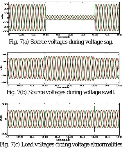
The system is subjected to sag of 0.84p.uand swell of 1.2p.u where 208V is treated as 1p.u. This amount of sag lasts for 0.1sec i.e., from 0.15sec to 0.35 sec. This is shown in figure 7(a) and 7(b).
Fig. 7(a) Source voltages during voltage sag.
Fig. 7(b) Source voltages during voltage swell.
Fig. 7(c) Load voltages during voltage abnormalities
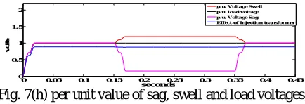
It is observed from the fig. 7(c) that even the supply voltage is varied; load voltages can be maintained constant around 1p.u. throughout the time duration, which is due to the injected voltages as in figure 7(d) and 7(e) during voltage sag and swells respectively. It can be observed from figure 7(f) and 7(g), voltages of supply and the injected voltages are in-phase with each other. This is due to the positive pulses by the controller to the IGBT modules of DVR since the injected voltage error between the reference generated voltages and the measured injected voltages are positive during sag time duration and negative pulses by the controller to the IGBT modules of DVR during swell duration. It can be observed that even during voltage abnormalities, per unit values of supply voltages with sag, swell, and load voltages are shown in figure 7(h) in which load voltage remains constant.
Fig. 7(d) Injected voltages during voltage sag by Dynamic voltage restorer
Fig. 7(e) Injected voltages during voltage swell by Dynamic voltage restorer
0 0.05 0.1 0.15 0.2 0.25 0.3 0.35 0.4 0.45
-300 -200 -100 0 100 200 300
seconds
v
o
lt
s
0 0.05 0.1 0.15 0.2 0.25 0.3 0.35 0.4 0.45
-400 -200 0 200 400
seconds
v
o
lt
s
0 0.05 0.1 0.15 0.2 0.25 0.3 0.35 0.4 0.45
-500 0 500
seconds
v
o
lt
s
0 0.05 0.1 0.15 0.2 0.25 0.3 0.35 0.4 0.45 -300
-200 -100 0 100 200 300
seconds
v
o
lt
s
0 0.05 0.1 0.15 0.2 0.25 0.3 0.35 0.4 0.45
-150 -100 -50 0 50 100 150
seconds
v
o
lt
Fig. 7(f) Showing In-phase compensation during voltage sag
Fig. 7(g) Showing In-phase compensation during voltage swell
Injection transformer is connected in series with a supply-load line to inject the compensation voltages and for the purpose of electrical isolation of DVR with the grid. Bypass equipment is provided between the inverter and secondary of series injection transformer for the load current to be ensured during a fault, overload and in service conditions. This means in normal condition the DVR may either go into short circuit operation or inject small voltage to compensate the voltage drop and phase shift on transformer reactance or losses, depending on short circuit impedance of the injecting transformer. The effect of injection transformer with high impedance values is included in fig 7(h).
Fig. 7(h) per unit value of sag, swell and load voltages.
The above simulation result can also be achieved from the reduced energy voltage rating (Case II) than conventional methodology (Case I)and we have achieved our aim to maintain constant load voltage with a minimum voltage rating of energy storage device (super-capacitor) of 30V instead of 144V as used in the conventional method.
Fig. 7(i) DC-Link voltages during sag and swell for both Case I and Case II
Fig. 7(j) Energy Storage Supply (UCAP) voltages during sag and swell for Case I and Case II
In Case I, during sag and swell conditions, DC-link voltage is maintained constant 260V and modulation index is varied accordingly to supply voltage, whereas in Case II, Vref is generated according to sag or swell. During sag
condition, Vref is positive and injected voltages are in-phase with supply voltages and during swell condition, Vref is
negative and injected voltages are out of phase to compensate the voltage swell. This can be shown in figure 7(i). Energy storage device (UCAP) supply voltages during voltage sag and swell for both case I and case II are shown in figure 7(j), which indicates 30V is enough to achieve constant load voltages by using variable DC link control. Here modulation index is fixed at 0.99 and turn’s ratio of injection transformer is 200/300V, satisfying eq (5).
0 0.05 0.1 0.15 0.2 0.25 0.3 0.35 0.4 0.45 -300 -200 -100 0 100 200 300 seconds v o lt s
0 0.05 0.1 0.15 0.2 0.25 0.3 0.35 0.4 0.45
-400 -200 0 200 400 seconds v o lt s
0 0.05 0.1 0.15 0.2 0.25 0.3 0.35 0.4 0.45
0 0.5 1 1.5 2 seconds v o lt s
p.u. Voltage Swell p.u. l oad voltage p.u. Voltage Sag Effect of Injection transformer
0 0.05 0.1 0.15 0.2 0.25 0.3 0.35 0.4 0.45
-200 0 200 400 600 seconds v o lt s
Ca se I:-During sag a nd swell Ca se II:-During Sag Ca se II:-During Swell
Compensation of voltage for Sensitive load by Variable DC-Link Voltage Control:-
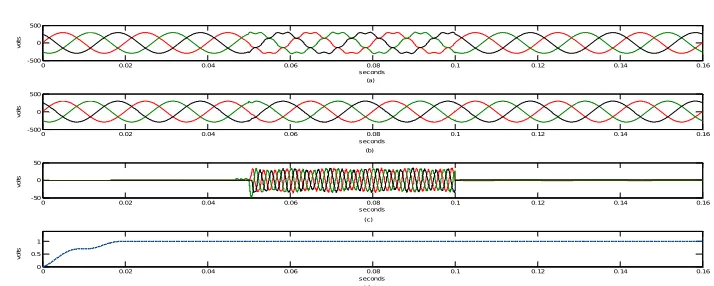
If a three phase thyristor controlled load is connected to proposed system between 0.05 sec. to 0.10 sec, it is observed that load voltages are almost maintained constant with less distortion, as the series DVR inject the compensation voltages with 30V super-capacitor module as shown in figure 7(k).
Fig. 7(k) output of load voltages connected to sensitive load without the UCAP-DVR system. (b) The output of load voltages connected to a sensitive load with the UCAP-DVR system. (c) Injected voltages to compensate voltage distortions. (d) Source (blue) and Load (red) RMS voltages with voltage harmonics.
Compensation of voltage harmonics by Variable DC-Link Voltage Control:-
Fig. 7(l) output of load voltages without the UCAP-DVR system. (b) The output of load voltages with theUCAP-DVR system. (c) Injected voltages to compensate voltage harmonics. (d) Source (blue) and Load (green) RMS voltages with voltage harmonics.
The Source voltages with harmonics are connected to proposed system between 0.05 sec. to 0.10 sec results in voltage distortion as shown in fig. 7(l) and we observed that load voltages are maintained constant with less distortion, as the series DVR inject the compensate voltages as shown in figure Here the time scale is reduced to 0.16 sec. inorder to have convenience view of voltages and load is connected between 0.05 sec. to 0.10 sec.
VI. CONCLUSION
In this paper power quality improvement is studied by integrating energy storage device to dynamic voltage restorer using stiff dc voltage and proposed a scheme in which dc-link voltage is varied. Energy storage device voltage rating is reduced from 144V to 30V with proposed scheme and complexity of the circuit is reduced. Thus, we achieve the transfer of control from AC to DC side. The performance of DC-link control scheme is studied for sag, swell, sensitive load, voltage harmonics and effect of injection transformer is discussed.
0 0. 02 0.04 0.06 0. 08 0.1 0.12 0. 14 0.16
-400 -200 0 200 400 seconds v o lt s
0 0. 02 0.04 0.06 0. 08 0.1 0.12 0. 14 0.16
-400 -200 0 200 400 seconds v o lt s
0 0. 02 0.04 0. 06 0.08 0.1 0. 12 0.14 0.16
-100 -50 0 50 100 seconds v o lt s
0 0.02 0. 04 0.06 0.08 0.1 0.12 0.14 0. 16
0 0.5 1 seconds vo lt
s load rms volt age
source rms voltage (a)
(b)
(c)
0 0.02 0.04 0.06 0.08 0.1 0.12 0.14 0.16
-500 0 500 seconds v o lt s
0 0.02 0.04 0.06 0.08 0.1 0.12 0.14 0.16
-500 0 500 seconds v o lt s
0 0.02 0.04 0.06 0.08 0.1 0.12 0.14 0.16
-50 0 50 seconds v o lt s
0 0.02 0.04 0.06 0.08 0.1 0.12 0.14 0.16
REFERENCES
[1] W. Edward Reid,”Power Quality Issues-Standards and Guidelines”, IEEE Transactions on Industry Applications, vol. 32, no. 3, May/June 1996.
[2] M. H. J. Bollen,” What is Power Quality”, Electric Power System Research 66(2003),pp. 5-14
[3] Alexander Kusko, ”Quality of Electric Power”, IEEE Transactions on industry and general applications, vol. IGA-3, no. 6, Nov/dec 1967. [4] Philip P. Barker, Thomas A. Short, Clayton W. Burns, James J. Burke, Cheryl A. Warren, Jerome J.Siewierski, “Power Quality Monitoring of a
distribution System”, IEEE Transactions on power delivery, vol. 9, no.2, April 1994.
[5] Muhammad A. Saqib, Ali Z. Saleem, “Power-quality issues and the need for reactive power compensation in the grid integration of wind power”, Renewable and Sustainable Energy Reviews 43 (2015) pp.51-64.
[6] Tomasz Adrikowski, David Bula, Marian Pasko, “The use of p-q control in single-phase active power filter for dynamic reactive power compensation”, doi:10.15199/48.2016.02.34.
[7] Irene Yu-Hua Gu, Emmanouil Styvaktakis, ”Bridge the gap: signal processing for power quality applications”, Electric Power System Research 66(2003) 83-96.
[8] N. H. Woodley, L. Morgan, and A. Sundaram, “Experience with an inverter-based dynamic voltage restorer,” IEEE Transactions on Power Delivery, vol. 14, no.3, pp.1181-1186, jul.1999.
[9] J. G. Nielson, and F. Blaabjerg, “A Detailed Comparison of system topologies for Dynamic Voltage Restorers”, IEEE Transactions on industry applications, vol. 41, no. 5, pp. 1272-1280, September/October 2005.
[10] S. S. Choi, B. H. Li, and D. M. Vilathgamuwa, ”Dynamic voltage restoration with minimum energy injection,” IEEE Transactions on Power Systems, vol. 15, no. 1, pp. 51-57, Feb. 2000.
[11] D. M. Vilathgamuwa, A. A. D. R. Perera, and S. S. Choi, “Voltage sag compensation with energy optimized dynamic voltage restorer,” IEEE Transactions on Power Delivery, vol. 18, no. 3, pp. 928-936, July 2003.
[12] Arindam Ghosh, Gerard Ledwich, “Compensation of distribution system voltage using DVR”, IEEE Transactions on power delivery, vol. 17, no. 4, pp. 1030-1036, October 2002.
[13] P. Roncero-Sanchez, Enrique Acha, Jose Enrique Ortega-Calderon, V. Feliu, and A.G. Cerrada, “A Versatile Control of a Dynamic Voltage Restorer for Power-Quality Improvement”, IEEE Transactions on Power delivery, vol. 24, no. 1, January 2009.
[14] Ebrahim Babaei, M. F. Kangarlu, M. Sabahi, “Mitigation of Voltage Disturbances Using Dynamic Voltage Restorer Based on Direct Converters”, IEEE Transactions on Power Delivery, vol. 25, no. 4, October 2010.
[15] H. Chen, T. N. Cong, Wei Yang, C. Tan, Y. Li, Y. Ding, “Progress in anelectrical energy storage system: A. Critical review”, Progress in Natural Science 19 (2009) pp. 291-312.
[16] A. Evans, V. Strezov, Tim J. Evans, “Assessment of utility energy storage for increased renewable energy penetration”, Renewable and sustainable Energy reviews 16 (2012) pp.4141-4147.
[17] S. Buller, M. Thele, R. W. De Doncker, and E. Karden, ”Impedance-Based Simulation models”, IEEE Industry Applications Magazine, Mar | Apr 2005.
[18] J. ArriUaga, D. A. Bradley, P. S. Bndger, Power System Harmonics (First Edition, John Wiley, and Sons, New York, 1985) [19] Fang Z. Peng,”Harmonic sources and filtering approaches”, IEEE Industry applications Magazine, July/August 2001.
[20] Deepak Somayajula, Mariesa L.Crow, ”An Integrated Dynamic Voltage Restorer-Ultra capacitor Design for Improving Power Quality of the distribution grid”, IEEE Transactions of Sustainable Energy, vol.6, no. 2,pp.616-624, April 2015.
[21] R. W. Erickson and D. Maksimovic, Fundamentals of Power Electronics, 2nded. Norwell, MA, USA: Kluwer, 2001.
[22] H. Akali, E. H. Watanabe, and M. Aredes, “Instantaneous Reactive power Theory and Applications to Power Conditioning”, 1st ed. Hoboken, NJ,USA: Wiley, Piscataway, NJ, USA: IEEE Press, 2007.